US6700754B2 - Oxidized copper (Cu) spacer between free and pinned layer for high performance spin valve applications - Google Patents
Oxidized copper (Cu) spacer between free and pinned layer for high performance spin valve applications Download PDFInfo
- Publication number
- US6700754B2 US6700754B2 US09/846,735 US84673501A US6700754B2 US 6700754 B2 US6700754 B2 US 6700754B2 US 84673501 A US84673501 A US 84673501A US 6700754 B2 US6700754 B2 US 6700754B2
- Authority
- US
- United States
- Prior art keywords
- layer
- spin valve
- valve sensor
- pinned
- spacer
- Prior art date
- Legal status (The legal status is an assumption and is not a legal conclusion. Google has not performed a legal analysis and makes no representation as to the accuracy of the status listed.)
- Expired - Fee Related, expires
Links
Images


Classifications
-
- B—PERFORMING OPERATIONS; TRANSPORTING
- B82—NANOTECHNOLOGY
- B82Y—SPECIFIC USES OR APPLICATIONS OF NANOSTRUCTURES; MEASUREMENT OR ANALYSIS OF NANOSTRUCTURES; MANUFACTURE OR TREATMENT OF NANOSTRUCTURES
- B82Y25/00—Nanomagnetism, e.g. magnetoimpedance, anisotropic magnetoresistance, giant magnetoresistance or tunneling magnetoresistance
-
- G—PHYSICS
- G01—MEASURING; TESTING
- G01R—MEASURING ELECTRIC VARIABLES; MEASURING MAGNETIC VARIABLES
- G01R33/00—Arrangements or instruments for measuring magnetic variables
- G01R33/02—Measuring direction or magnitude of magnetic fields or magnetic flux
- G01R33/06—Measuring direction or magnitude of magnetic fields or magnetic flux using galvano-magnetic devices
- G01R33/09—Magnetoresistive devices
- G01R33/093—Magnetoresistive devices using multilayer structures, e.g. giant magnetoresistance sensors
-
- B—PERFORMING OPERATIONS; TRANSPORTING
- B82—NANOTECHNOLOGY
- B82Y—SPECIFIC USES OR APPLICATIONS OF NANOSTRUCTURES; MEASUREMENT OR ANALYSIS OF NANOSTRUCTURES; MANUFACTURE OR TREATMENT OF NANOSTRUCTURES
- B82Y10/00—Nanotechnology for information processing, storage or transmission, e.g. quantum computing or single electron logic
-
- G—PHYSICS
- G11—INFORMATION STORAGE
- G11B—INFORMATION STORAGE BASED ON RELATIVE MOVEMENT BETWEEN RECORD CARRIER AND TRANSDUCER
- G11B5/00—Recording by magnetisation or demagnetisation of a record carrier; Reproducing by magnetic means; Record carriers therefor
- G11B5/012—Recording on, or reproducing or erasing from, magnetic disks
-
- G—PHYSICS
- G11—INFORMATION STORAGE
- G11B—INFORMATION STORAGE BASED ON RELATIVE MOVEMENT BETWEEN RECORD CARRIER AND TRANSDUCER
- G11B5/00—Recording by magnetisation or demagnetisation of a record carrier; Reproducing by magnetic means; Record carriers therefor
- G11B5/127—Structure or manufacture of heads, e.g. inductive
- G11B5/33—Structure or manufacture of flux-sensitive heads, i.e. for reproduction only; Combination of such heads with means for recording or erasing only
- G11B5/39—Structure or manufacture of flux-sensitive heads, i.e. for reproduction only; Combination of such heads with means for recording or erasing only using magneto-resistive devices or effects
- G11B5/3903—Structure or manufacture of flux-sensitive heads, i.e. for reproduction only; Combination of such heads with means for recording or erasing only using magneto-resistive devices or effects using magnetic thin film layers or their effects, the films being part of integrated structures
Definitions
- the present invention relates to magnetoresistive read sensors for reading signals recorded in a magnetic medium, and more particularly, this invention relates to tailoring a spacer of a spin valve magnetoresistive read sensor for improving operating characteristics.
- Computer systems generally utilize auxiliary memory storage devices having media on which data can be written and from which data can be read for later use.
- a direct access storage device disk drive
- disk drive incorporating rotating magnetic disks is commonly used for storing data in magnetic form on the disk surfaces. Data is recorded on concentric, radially spaced tracks on the disk surfaces. Magnetic heads including read sensors are then used to read data from the tracks on the disk surfaces.
- magnetoresistive read sensors In high capacity disk drives, magnetoresistive read sensors, commonly referred to as MR heads, are the prevailing read sensors because of their capability to read data from a surface of a disk at greater linear densities than thin film inductive heads.
- An MR sensor detects a magnetic field through the change in the resistance of its MR sensing layer (also referred to as an “MR element”) as a function of the strength and direction of the magnetic flux being sensed by the MR layer.
- the conventional MR sensor operates on the basis of the anisotropic magnetoresistive (AMR) effect in which an MR element resistance varies as the square of the cosine of the angle between the magnetization of the MR element and the direction of sense current flowing through the MR element.
- AMR anisotropic magnetoresistive
- GMR giant magnetoresistance
- the resistance of the MR sensing layer varies as a function of the spin-dependent transmission of the conduction electrons between magnetic layers separated by a non-magnetic layer (spacer) and the accompanying spin-dependent scattering which takes place at the interface of the magnetic and non-magnetic layers and within the magnetic layers.
- GMR sensors using only two layers of ferromagnetic material separated by a layer of non-magnetic electrically conductive material are generally referred to as spin valve (SV) sensors manifesting the GMR effect (SV effect).
- SV spin valve
- one of the ferromagnetic layers referred to as the pinned layer
- an antiferromagnetic layer e.g., NiO, FeMn, PtMn
- the magnetization of the other ferromagnetic layer referred to as the free layer, however, is not fixed and is free to rotate in response to the field from the recorded magnetic medium (the signal field).
- the spin valve effect varies as the cosine of the angle between the magnetization of the pinned layer and the magnetization of the free layer.
- Recorded data can be read from a magnetic medium because the external magnetic field from the recorded magnetic medium causes a change in the direction of magnetization in the free layer, which in turn causes a change in resistance of the spin valve sensor and a corresponding change in the sensed current or voltage.
- the AMR effect is also present in the spin valve sensor free layer.
- FIG. 1 shows a typical spin valve sensor 100 (not drawn to scale) comprising end regions 104 and 106 separated by a central region 102 .
- the central region 102 has defined edges and the end regions are contiguous with and abut the edges of the central region.
- a free layer (free ferromagnetic layer) 110 is separated from a pinned layer (pinned ferromagnetic layer) 120 by a non-magnetic, electrically-conducting spacer 115 .
- the spacer layer 115 separating magnetic free layer 110 and pinned layer 120 is critical for the performance of any type of spin valve device. Variety of spacer materials have been evaluated in the past, and copper (Cu) is commonly accepted as leading to the best spin valve characteristics, and is commonly used in device applications.
- Cu copper
- the magnetization of the pinned layer 120 is fixed through exchange coupling with an antiferromagnetic (AFM) layer 125 .
- Free layer 110 , spacer 115 , pinned layer 120 and the AFM layer 125 are all formed in the central region 102 .
- Leads 140 and 145 formed over hard bias layers 130 and 135 respectively, provide electrical connections for the flow of the sensing current I s from a current source 160 to the MR sensor 100 .
- Sensor 170 is connected to leads 140 and 145 senses the change in the resistance due to changes induced in the free layer 110 by the external magnetic field (e.g., field generated by a data bit stored on a disk).
- FIG. 2A shows an exemplary AP-Pinned spin valve sensor 200 (not drawn to scale).
- Spin valve sensor 200 has end regions 202 and 204 separated from each other by a central region 206 .
- AP-pinned spin valve sensor 200 comprises a Ni-Fe free layer 225 separated from a laminated AP-pinned layer 210 by a copper spacer layer 220 .
- the magnetization of the laminated AP-pinned layer 210 is fixed by an AFM layer 208 , or pinning layer, which is made of NiO.
- the laminated AP-pinned layer 210 includes a first ferromagnetic layer 212 (PF 1 ) of cobalt and a second ferromagnetic layer 216 (PF 2 ) of cobalt separated from each other by a ruthenium (Ru) anti-parallel coupling layer 214 .
- the AMF layer 208 , AP-pinned layer 210 , copper spacer 220 , free layer 225 and a cap layer 230 are all formed sequentially in the central region 206 .
- Hard bias layers 235 and 240 formed in end regions 202 and 204 , provides longitudinal biasing for the free layer 225 .
- Electrical leads 245 and 250 are also formed in end regions 202 and 204 , respectively, to provide electrical current from a current source (not shown) to the spin valve sensor 200 .
- Various parameters of a spin valve sensor may be used to evaluate the performance thereof. For example, the structure sheet resistance (R), GMR ratio ( ⁇ R/R), and ferromagnetic interlayer coupling field (H f ) are all performance indicators.
- ⁇ R/R which is defined as (R AP ⁇ R p )/R p , where R AP is the anti-parallel resistance and R p is the parallel resistance.
- the GMR effect depends on the angle between the magnetizations of the free and pinned layers. More specifically, the GMR effect is proportional to the cosine of the angle B between the magnetization vector of the pinned layer (M p ) and the magnetization vector of the free layer (M F ) (Note FIGS. 2 B and 2 C).
- the electron scattering and therefore the resistance is maximum when the magnetizations of the pinned and free layers are antiparallel, i.e., majority of the electrons are scattered as they try to cross the boundary between the MR layers.
- electron scattering and therefore the resistance is minimum when the magnetizations of the pinned and free layers are parallel; i.e., majority of electrons are not scattered as they try to cross the boundary between the MR layers.
- the thickness of the spacer layer is traditionally chosen to be less than the mean free path of conduction electrons through the spin valve sensor. With this arrangement, a portion of the conduction electrons are scattered by the interfaces of the spacer layer with the pinned and free layers. As mentioned earlier, changes in the scattering of the conduction electrons change the resistance of the spin valve sensor in proportion to cos ⁇ , where ⁇ is the angle between the magnetizations of the pinned and free layers.
- a spin valve sensor system and method for fabricating the same. Included is a free layer and a pinned layer with a spacer layer disposed between the free layer and the pinned layer. Such spacer layer is oxidized for improving operational characteristics of the spin valve sensor.
- the spacer layer may include CuO x .
- the characteristics that are improved by the oxidation may include R, ⁇ R/R, and/or H f .
- the spacer layer may be constructed utilizing physical vapor deposition (PVD) sputtering.
- the spacer layer may be oxidized utilizing in-situ post-oxidation, reactive sputtering in oxygen, or a combination thereof.
- the spacer layer may be oxidized in an environment characterized between 1E-4 and 1E-2 Torr*min.
- the spacer layer may be oxidized in an environment characterized between 5 ⁇ 10 ⁇ 8 and 5 ⁇ 10 ⁇ 7 Torr.
- the spacer layer may be oxidized during and/or after being constructed. Further, the spacer layer may comprise a plurality of oxidized sub-layers. It should be noted that the spin valve sensor may take any form such as a top spin valve, a bottom spin valve, a dual spin valve, and/or an anti-parallel (AP)-pinned spin valve sensor.
- AP anti-parallel
- a method may be provided for fabricating the spin valve sensor. During such method for a bottom spin valve, a pinned layer is deposited, and a spacer layer deposited on the pinned layer. Further, a free layer is deposited on the spacer layer. As set forth earlier, the spacer layer is oxidized for improving operational characteristics of the spin valve sensor.
- FIG. 1 is a schematic diagram of the cross-section of a prior art spin valve sensor
- FIG. 2A shows an AP-Pinned spin valve sensor in accordance with the prior art
- FIGS. 2B and 2C illustrate a perspective of the free and pinned layers, and a diagram of the magnetization vectors, respectively, of a prior art spin valve sensor
- FIG. 3 is a perspective drawing of a magnetic recording disk drive system
- FIG. 4 is a schematic diagram of the cross-section of the preferred spin valve sensor of the present invention.
- FIG. 5A is a schematic diagram of the cross-section of a thin film structure in accordance with the preferred embodiment of the present invention.
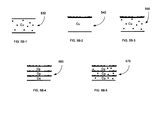
- FIGS. 5B-1, 2 , 3 , 4 and 5 show various exemplary embodiments regarding the manner in which the Cu of the spacer layer may be oxidized in accordance with the present invention.
- FIGS. 6 and 7 illustrate an exemplary comparison of optimized spin valve characteristics without Cu oxidation and with an increasing degree of Cu oxidation.
- FIG. 3 there is shown a disk drive 300 embodying the present invention.
- a disk drive 300 embodying the present invention.
- at least one rotatable magnetic disk 312 is supported on a spindle 314 and rotated by a disk drive motor 318 .
- the magnetic recording media on each disk is in the form of an annular pattern of concentric data tracks (not shown) on disk 312 .
- At least one slider 313 is positioned on the disk 312 , each slider 313 supporting one or more magnetic read/write heads 321 where the head 321 incorporates the MR sensor of the present invention. As the disks rotate, slider 313 is moved radially in and out over disk surface 322 so that heads 321 may access different portions of the disk where desired data are recorded. Each slider 313 is attached to an actuator arm 319 by way of a suspension 315 . The suspension 315 provides a slight spring force which biases slider 313 against the disk surface 322 . Each actuator arm 319 is attached to an actuator 327 .
- the actuator 327 as shown in FIG. 3 may be a voice coil motor (VCM).
- the VCM comprises a coil movable within a fixed magnetic field, the direction and speed of the coil movements being controlled by the motor current signals supplied by controller 329 .
- the rotation of disk 312 generates an air bearing between slider 313 and disk surface 322 which exerts an upward force or lift on the slider.
- the air bearing thus counter-balances the slight spring force of suspension 315 and supports slider 313 off and slightly above the disk surface by a small, substantially constant spacing during normal operation.
- control unit 329 The various components of the disk storage system are controlled in operation by control signals generated by control unit 329 , such as access control signals and internal clock signals.
- control unit 329 comprises logic control circuits, storage and a microprocessor.
- the control unit 329 generates control signals to control various system operations such as drive motor control signals on line 323 and head position and seek control signals on line 328 .
- the control signals on line 328 provide the desired current profiles to optimally move and position slider 313 to the desired data track on disk 312 .
- Read and write signals are communicated to and from read/write heads 321 by way of recording channel 325 .
- disk storage systems may contain a large number of disks and actuators, and each actuator may support a number of sliders.
- FIG. 4 there is shown an air bearing surface (ABS) view of the spin valve sensor 400 (not drawn to scale) having the structure of Underlayer/PtMn/CoFe/Ru/CoFe/Spacer/CoFe/NiFe/Ta and manufactured, using a sputter deposition process, according to the preferred embodiment of the present invention.
- Spin valve sensor 400 comprises end regions 404 and 406 separated by a central region 402 .
- a free layer (free ferromagnetic layer) 410 comprising a NiFe layer and/or a thin CoFe layer, is separated from a pinned layer (pinned ferromagnetic layer) 420 , comprising a Ru layer and two thin CoFe layers, by a non-magnetic, electrically-conducting spacer layer 415 .
- Such electrically-conducting spacer layer 415 may be constructed from copper, Cu.
- such copper spacer layer 415 is oxidized in order to improve operational characteristics. More information regarding such improvement will be set forth in greater detail during reference to FIGS. 5-7.
- the magnetization of the pinned layer 420 is fixed by an antiferromagnetic (AFM) layer 425 .
- An underlayer 429 , AFM layer 425 , pinned layer 420 , spacer layer 415 , free layer 410 , and a cap layer 408 are all formed in that order in the central region 402 .
- the underlayer 429 or seed layer is any layer(s) deposited to modify the crystallographic texture or grain size of the subsequent layers, and may not be needed depending on the substrate.
- the spin valve sensor 400 further comprises layers 430 and 435 formed in the end regions 404 and 406 , respectively, for providing a longitudinal bias field to the free layer 410 to ensure a single magnetic domain state in the free layer 410 .
- Layers 430 and 435 preferably made of hard magnetic material such as CoPtCr, are deposited and magnetically aligned at room temperature according to the well known methods established in the prior art.
- Lead layers 440 and 445 are formed over hard bias layers 430 and 435 in the end regions 404 and 406 , respectively, by the methods known in the prior art.
- Leads 440 and 445 provide electrical connections for the flow of the sensing current I s from a current source 460 to the spin valve sensor 400 .
- the sensor 470 is connected to leads 440 and 445 senses the change in the resistance due to changes induced in the free layer 410 by the external magnetic field (e.g., field generated by a data bit stored on a disk).
- spin valve sensors may contain differing layers of varying materials for accomplishing similar results.
- the spin valve sensor may include a top spin valve, a bottom spin valve, a dual spin valve, and/or any other type of spin valve per the desires of the user.
- the sputter deposition process for fabrication of the central region 402 of FIG. 4 of spin valve sensor 400 is shown (not to scale) with deposition on a substrate 500 of suitable underlayer 501 materials including NiFeCr and NiFe. Thereafter, an antiferromagnetic (AFM) pinning layer 507 is deposited.
- the preferred composition of the AFM layer 507 is a PtMn composition 510 .
- PtMn the notation “PtMn” (or any other combination of materials) refers to any desirable amount of either materials, i.e. Pt—Mn.
- a pinned layer 511 is subsequently deposited in direct contact and overlaying the pinning layer 507 .
- the pinned layer 511 includes a CoFe layer 512 followed by a Ru layer 514 and another CoFe layer 516 .
- a spacer layer 518 is deposited.
- the spacer layer 518 includes Cu. While such Cu may be deposited in any desired manner, physical vapor deposition (PVD) sputtering may be utilized in one embodiment. PVD sputtering is commonly used for depositing metal films and the like onto substrate surfaces.
- PVD sputtering is commonly used for depositing metal films and the like onto substrate surfaces.
- a planar target is typically positioned within a chamber, in spaced apart and symmetrical counterfacing relation with the substrate. The target is made of the material that is to be sputter deposited onto the substrate surface. Emission-inducing energy is applied to the active face of the target in the form, for example, of a plasma containing accelerated argon ions.
- the active face of the target emits small particles composed of the target material.
- the emitted particles follow a generally linear trajectory from their point of emission on the target surface to a collision point on the counterfacing surface of the substrate.
- Physical adhesion mechanisms cause the target particles to bond to the surface of the substrate.
- the spacer layer 518 includes oxidized Cu, or CuO x .
- the Cu may be oxidized using any desired method.
- the oxidized Cu spacer may be incorporated into a spin valve stack by in-situ intra-deposition and/or post-deposition oxidation of a Cu metal layer. Oxidation can be applied to a whole spacer layer or only a part of it (thickness-wise), with the magnitude of observed effects roughly scaling with the fraction of oxidized material built into the structure.
- the term “in-situ” is often used since the substrate never leaves the vacuum of one machine.
- the spacer layer may be oxidized in an environment characterized between 1E-4 and 1E-2 Torr*min.
- reactive sputtering may be carried out in atmosphere with oxygen background.
- the spacer layer 518 may be oxidized in an environment characterized between 5 ⁇ 10 ⁇ 8 and 5 ⁇ 10 ⁇ 7 Torr. It should be noted that the spacer layer 518 may be oxidized utilizing in-situ post-oxidation, reactive sputtering, or a combination thereof. Additional information regarding exemplary methods of oxidizing the spacer layer 518 will be set forth in greater detail during reference to FIGS. 5B-1, 2 , 3 , 4 and 5 .
- the free layer 519 comprises a CoFe layer 520 and/or a NiFe layer 522 .
- the cap layer 523 may include a Ta composition 524 . This completes processing of the central region of the spin valve structure of the preferred embodiment of the present invention.
- end regions are formed which include depositing horizontal bias layers and leads according to the well known methods established in the prior art.
- spin valve sensor structure of the present invention and the accompanying illustration of FIG. 5A are for representation purposes only.
- Such spin valve sensor structure is that which was used to produce the analysis data set forth hereinbelow.
- Such data shows improvements associated with applying the principles of the improved spacer of the present invention. It should be noted, however, that other spin valve sensor structures including differing layers of varying materials may be employed while still achieving improvements unique to the improved spacer.
- FIGS. 5B-1, 2 , 3 , 4 and 5 show various exemplary embodiments (not drawn to scale) regarding the manner in which the Cu of the spacer layer 518 may be oxidized.
- a first embodiment 530 is shown where the Cu of the spacer layer is oxidized during deposition. Resulting is the formation of CuOx amorphous phase as deposited film.
- FIG. 5B-2 illustrates a second embodiment 540 where the Cu of the spacer layer is oxidized after the Cu is deposited. As shown, the oxidation takes place on an upper surface of the spacer layer.
- FIG. 5B-3 shows the result of combining the approaches of FIGS. 5B-1 and 5 B- 2 in a third embodiment 550 .
- a fourth embodiment 560 is shown with a plurality of stacked sub-layers of Cu that are oxidized in the manner set forth in the second embodiment 540 of FIG. 5B-2.
- a fifth embodiment 570 is shown in FIG. 5B-5 wherein a plurality of stacked sub-layers of Cu that are oxidized in the manner set forth in the first and second embodiments 530 , 540 of FIG. 5B-1 and 5 B- 2 , respectively.
- the foregoing exemplary embodiments are for illustrative purposes only, and that any desired method may be used to afford the spacer layer constructed at least in part with CuO x .
- Table 1 shows the giant magnetoresistive (GMR) coefficients ( ⁇ R/R), structure sheet resistances (R), and interlayer couplings (H f ) for the prior art and present invention spin valve structures taken from FIG. 5 A.
- GMR giant magnetoresistive
- R structure sheet resistances
- H f interlayer couplings
- FIGS. 6 and 7 illustrate an exemplary comparison of optimized spin valve characteristics without Cu oxidation (see sample #1) and with increasing degrees of Cu oxidation (see samples #2 through #4).
- Table 1 and FIGS. 6 and 7 significant improvement of all critical spin valve characteristics is exhibited, with the overall increase in the figure of merit AR from 1.55 Ohm/sq. to 2.17 Ohm/sq or higher. (40% increase).
- the improvement results from both direct and indirect oxidation-related effects associated with the oxidized Cu spacer layer.
- a direct increase in ⁇ R/R and R, and decrease in H f is induced by oxidation-related changes in spin valve microchemistry and microstructure.
- Table 3 shows a correlation between increase in R of the spin valve structure (similar to that used in Table 1) and the level of oxygen background used during the CuO x spacer deposition.
- Table 3 shows the resistivity of CuO x in ⁇ 600 A thick films reactively sputtered in Ar with various percentages of oxygen. It should be noted that the increase in R observed at higher oxidation levels is due at least in part to the increased resistivity of the CuO x material.
- the fabrication methods of the preferred embodiment and the alternative embodiments described herein may be used to fabricate spin valve sensors having any other layered structure, i.e. underlayer/pinned layer/spacer/free layer. Further, it should be noted that the various principles of the present invention may be applicable in a very broad range of spin valve sensor devices.
Landscapes
- Engineering & Computer Science (AREA)
- Chemical & Material Sciences (AREA)
- Nanotechnology (AREA)
- Physics & Mathematics (AREA)
- Crystallography & Structural Chemistry (AREA)
- Condensed Matter Physics & Semiconductors (AREA)
- General Physics & Mathematics (AREA)
- Manufacturing & Machinery (AREA)
- Mathematical Physics (AREA)
- Theoretical Computer Science (AREA)
- Hall/Mr Elements (AREA)
- Magnetic Heads (AREA)
Abstract
Description
| TABLE 1 | ||||||
| R · Ω/ | Dr [R × (ΔR/R)], | |||||
| sq | Hce, Oe | Hf, Oe | ΔR/R % | Ω/sq | ||
| Cu spacer layer | 14.6 | 4.7 | 9.4 | 10.64 | 1.55 |
| CuOx spacer | 17.7 | 4.6 | −6.7 | 12.24 | 2.17 |
| layer | |||||
| CuOx spacer | 18.3 | −3.6 | 13.3% | 2.4 | |
| layer-optimized | |||||
| embodiment | |||||
| TABLE 2 | |||
| % O2 | ρ, μΩcm | ||
| 0.00 | 3.6 | ||
| 1.20 | 686.5 | ||
| 3.6 | 5290.0 | ||
| 6.00 | 56954.5 | ||
| TABLE 3 | |||
| % O2 | R, Ω/sq | ||
| 0.12 | 18.4 | ||
| 0.23 | 18.7 | ||
| 0.46 | 19.7 | ||
Claims (21)
Priority Applications (1)
| Application Number | Priority Date | Filing Date | Title |
|---|---|---|---|
| US09/846,735 US6700754B2 (en) | 2001-04-30 | 2001-04-30 | Oxidized copper (Cu) spacer between free and pinned layer for high performance spin valve applications |
Applications Claiming Priority (1)
| Application Number | Priority Date | Filing Date | Title |
|---|---|---|---|
| US09/846,735 US6700754B2 (en) | 2001-04-30 | 2001-04-30 | Oxidized copper (Cu) spacer between free and pinned layer for high performance spin valve applications |
Publications (2)
| Publication Number | Publication Date |
|---|---|
| US20030021071A1 US20030021071A1 (en) | 2003-01-30 |
| US6700754B2 true US6700754B2 (en) | 2004-03-02 |
Family
ID=25298793
Family Applications (1)
| Application Number | Title | Priority Date | Filing Date |
|---|---|---|---|
| US09/846,735 Expired - Fee Related US6700754B2 (en) | 2001-04-30 | 2001-04-30 | Oxidized copper (Cu) spacer between free and pinned layer for high performance spin valve applications |
Country Status (1)
| Country | Link |
|---|---|
| US (1) | US6700754B2 (en) |
Cited By (3)
| Publication number | Priority date | Publication date | Assignee | Title |
|---|---|---|---|---|
| US20030123201A1 (en) * | 2002-01-02 | 2003-07-03 | International Business Machines Corporation | Method and apparatus for providing precise control of magnetic coupling field in NiMn top spin valve heads and amplitude enhancement |
| US20030128481A1 (en) * | 2002-01-10 | 2003-07-10 | Fujitsu Limited | Current-perpendicular-to-the-plane structure magnetoresistive head |
| US20060060466A1 (en) * | 2004-09-17 | 2006-03-23 | Anelva Corporation | Manufacturing Method And Manufacturing Apparatus Of Magnetoresistance Elements |
Families Citing this family (7)
| Publication number | Priority date | Publication date | Assignee | Title |
|---|---|---|---|---|
| DE10128135A1 (en) * | 2001-06-09 | 2002-12-19 | Bosch Gmbh Robert | Magneto-resistive layer arrangement used in a GMR sensor element, an AMR sensor element or a gradiometer comprises a non-magnetic electrically conducting intermediate layer arranged between magnetic layers, and a hard magnetic layer |
| JP3565268B2 (en) * | 2001-06-22 | 2004-09-15 | 株式会社東芝 | Magnetoresistive element, magnetic head, and magnetic reproducing device |
| US7265946B2 (en) * | 2003-04-30 | 2007-09-04 | Hitachi Global Storage Technologies Netherlands B.V. | Multilayer self-pinned structure for CPP GMR |
| JP4204385B2 (en) * | 2003-05-27 | 2009-01-07 | Tdk株式会社 | Thin film magnetic head |
| US7201827B2 (en) * | 2003-09-12 | 2007-04-10 | Headway Technologies, Inc. | Process and structure to fabricate spin valve heads for ultra-high recording density application |
| JP2006018862A (en) * | 2004-06-30 | 2006-01-19 | Hitachi Global Storage Technologies Netherlands Bv | Magnetoresistive head and manufacturing method thereof |
| US8373948B2 (en) * | 2008-04-28 | 2013-02-12 | Hitachi Global Storage Technologies Netherlands B.V. | Tunnel magnetoresistance (TMR) structures with MGO barrier and methods of making same |
Citations (17)
| Publication number | Priority date | Publication date | Assignee | Title |
|---|---|---|---|---|
| US5390061A (en) * | 1990-06-08 | 1995-02-14 | Hitachi, Ltd. | Multilayer magnetoresistance effect-type magnetic head |
| US5648885A (en) | 1995-08-31 | 1997-07-15 | Hitachi, Ltd. | Giant magnetoresistive effect sensor, particularly having a multilayered magnetic thin film layer |
| US5793279A (en) | 1996-08-26 | 1998-08-11 | Read-Rite Corporation | Methods and compositions for optimizing interfacial properties of magnetoresistive sensors |
| US5793207A (en) | 1996-10-09 | 1998-08-11 | International Business Machines Corporation | Disk drive with a thermal asperity reduction circuitry using a spin valve sensor |
| US5828531A (en) | 1996-09-18 | 1998-10-27 | International Business Machines Corporation | Spin valve sensor with enhanced magnetoresistance |
| US5828598A (en) | 1997-05-23 | 1998-10-27 | Motorola, Inc. | MRAM with high GMR ratio |
| US5869963A (en) | 1996-09-12 | 1999-02-09 | Alps Electric Co., Ltd. | Magnetoresistive sensor and head |
| US5880913A (en) | 1997-10-27 | 1999-03-09 | International Business Machines Corporation | Antiparallel pinned spin valve sensor with read signal symmetry |
| US5898612A (en) | 1997-05-22 | 1999-04-27 | Motorola, Inc. | Magnetic memory cell with increased GMR ratio |
| US5955211A (en) | 1996-07-18 | 1999-09-21 | Sanyo Electric Co., Ltd. | Magnetoresistive film |
| US5968676A (en) | 1997-06-05 | 1999-10-19 | Tdk Corporation | Magnetoresistance effect film and magnetoresistance effect type head |
| US5993566A (en) | 1997-09-03 | 1999-11-30 | International Business Machines Corporation | Fabrication process of Ni-Mn spin valve sensor |
| US6108177A (en) * | 1998-11-19 | 2000-08-22 | International Business Machines Corporation | Tunnel junction structure with FeX ferromagnetic layers |
| US6178074B1 (en) * | 1998-11-19 | 2001-01-23 | International Business Machines Corporation | Double tunnel junction with magnetoresistance enhancement layer |
| US6275363B1 (en) * | 1999-07-23 | 2001-08-14 | International Business Machines Corporation | Read head with dual tunnel junction sensor |
| US20020054463A1 (en) * | 2000-11-06 | 2002-05-09 | Fujitsu Limited | Spin-valve magneto-resistive element, magnetic head and magnetic storage apparatus |
| US6452761B1 (en) * | 2000-01-14 | 2002-09-17 | International Business Machines Corporation | Magneto-resistive and spin-valve sensor gap with reduced thickness and high thermal conductivity |
-
2001
- 2001-04-30 US US09/846,735 patent/US6700754B2/en not_active Expired - Fee Related
Patent Citations (17)
| Publication number | Priority date | Publication date | Assignee | Title |
|---|---|---|---|---|
| US5390061A (en) * | 1990-06-08 | 1995-02-14 | Hitachi, Ltd. | Multilayer magnetoresistance effect-type magnetic head |
| US5648885A (en) | 1995-08-31 | 1997-07-15 | Hitachi, Ltd. | Giant magnetoresistive effect sensor, particularly having a multilayered magnetic thin film layer |
| US5955211A (en) | 1996-07-18 | 1999-09-21 | Sanyo Electric Co., Ltd. | Magnetoresistive film |
| US5793279A (en) | 1996-08-26 | 1998-08-11 | Read-Rite Corporation | Methods and compositions for optimizing interfacial properties of magnetoresistive sensors |
| US5869963A (en) | 1996-09-12 | 1999-02-09 | Alps Electric Co., Ltd. | Magnetoresistive sensor and head |
| US5828531A (en) | 1996-09-18 | 1998-10-27 | International Business Machines Corporation | Spin valve sensor with enhanced magnetoresistance |
| US5793207A (en) | 1996-10-09 | 1998-08-11 | International Business Machines Corporation | Disk drive with a thermal asperity reduction circuitry using a spin valve sensor |
| US5898612A (en) | 1997-05-22 | 1999-04-27 | Motorola, Inc. | Magnetic memory cell with increased GMR ratio |
| US5828598A (en) | 1997-05-23 | 1998-10-27 | Motorola, Inc. | MRAM with high GMR ratio |
| US5968676A (en) | 1997-06-05 | 1999-10-19 | Tdk Corporation | Magnetoresistance effect film and magnetoresistance effect type head |
| US5993566A (en) | 1997-09-03 | 1999-11-30 | International Business Machines Corporation | Fabrication process of Ni-Mn spin valve sensor |
| US5880913A (en) | 1997-10-27 | 1999-03-09 | International Business Machines Corporation | Antiparallel pinned spin valve sensor with read signal symmetry |
| US6108177A (en) * | 1998-11-19 | 2000-08-22 | International Business Machines Corporation | Tunnel junction structure with FeX ferromagnetic layers |
| US6178074B1 (en) * | 1998-11-19 | 2001-01-23 | International Business Machines Corporation | Double tunnel junction with magnetoresistance enhancement layer |
| US6275363B1 (en) * | 1999-07-23 | 2001-08-14 | International Business Machines Corporation | Read head with dual tunnel junction sensor |
| US6452761B1 (en) * | 2000-01-14 | 2002-09-17 | International Business Machines Corporation | Magneto-resistive and spin-valve sensor gap with reduced thickness and high thermal conductivity |
| US20020054463A1 (en) * | 2000-11-06 | 2002-05-09 | Fujitsu Limited | Spin-valve magneto-resistive element, magnetic head and magnetic storage apparatus |
Cited By (6)
| Publication number | Priority date | Publication date | Assignee | Title |
|---|---|---|---|---|
| US20030123201A1 (en) * | 2002-01-02 | 2003-07-03 | International Business Machines Corporation | Method and apparatus for providing precise control of magnetic coupling field in NiMn top spin valve heads and amplitude enhancement |
| US7038891B2 (en) * | 2002-01-02 | 2006-05-02 | International Business Machines Corporation | Method and apparatus for providing precise control of magnetic coupling field in NiMn top spin valve heads and amplitude enhancement |
| US20030128481A1 (en) * | 2002-01-10 | 2003-07-10 | Fujitsu Limited | Current-perpendicular-to-the-plane structure magnetoresistive head |
| US20060060466A1 (en) * | 2004-09-17 | 2006-03-23 | Anelva Corporation | Manufacturing Method And Manufacturing Apparatus Of Magnetoresistance Elements |
| US20090139855A1 (en) * | 2004-09-17 | 2009-06-04 | Canon Anelva Corporation | Manufacturing method and manufacturing apparatus of magnetoresistance elements |
| US7731825B2 (en) * | 2004-09-17 | 2010-06-08 | Canon Anelva Corporation | Manufacturing apparatus of magnetoresistance elements |
Also Published As
| Publication number | Publication date |
|---|---|
| US20030021071A1 (en) | 2003-01-30 |
Similar Documents
| Publication | Publication Date | Title |
|---|---|---|
| US6600638B2 (en) | Corrosion resistive GMR and MTJ sensors | |
| US6947264B2 (en) | Self-pinned in-stack bias structure for magnetoresistive read heads | |
| US6127045A (en) | Magnetic tunnel junction device with optimized ferromagnetic layer | |
| US7413636B2 (en) | Method for manufacturing a dual spin valve sensor having a longitudinal bias stack | |
| US6175476B1 (en) | Synthetic spin-valve device having high resistivity anti parallel coupling layer | |
| US8133363B2 (en) | Dual magnetic tunnel junction sensor with a longitudinal bias stack | |
| US6038107A (en) | Antiparallel-pinned spin valve sensor | |
| US7505235B2 (en) | Method and apparatus for providing magnetostriction control in a freelayer of a magnetic memory device | |
| US6735058B2 (en) | Current-perpendicular-to-plane read head with an amorphous magnetic bottom shield layer and an amorphous nonmagnetic bottom lead layer | |
| US8373948B2 (en) | Tunnel magnetoresistance (TMR) structures with MGO barrier and methods of making same | |
| US6731477B2 (en) | Current-perpendicular-to-plane spin-valve sensor with metallic oxide barrier layer and method of fabrication | |
| US7333302B2 (en) | GMR sensor having an under-layer treated with nitrogen for increased magnetoresistance | |
| US6600184B1 (en) | System and method for improving magnetic tunnel junction sensor magnetoresistance | |
| US8107202B2 (en) | Magnetoresistive sensor with novel pinned layer structure | |
| US6788502B1 (en) | Co-Fe supermalloy free layer for magnetic tunnel junction heads | |
| US20020036876A1 (en) | Magnetoresistive element, method for manufacturing the same, and magnetic device using the same | |
| US11283006B1 (en) | Methods and apparatus of high moment free layers for magnetic tunnel junctions | |
| US7360297B2 (en) | Magnetoresistive sensor with antiparallel coupled lead/sensor overlap region | |
| US6954342B2 (en) | Underlayer for high amplitude spin valve sensors | |
| US6700754B2 (en) | Oxidized copper (Cu) spacer between free and pinned layer for high performance spin valve applications | |
| US6982854B2 (en) | Magnetoresistance effect device and magnetoresistance effect head comprising the same, and magnetic recording/reproducing apparatus | |
| US6765767B2 (en) | Magnetoresistive head on a side wall for increased recording densities | |
| US7145755B2 (en) | Spin valve sensor having one of two AP pinned layers made of cobalt | |
| US6870716B2 (en) | Free layer and design for higher areal density | |
| US20090168271A1 (en) | Dual-layer free layer in a tunneling magnetoresistance (tmr) element having different magnetic thicknesses |
Legal Events
| Date | Code | Title | Description |
|---|---|---|---|
| AS | Assignment |
Owner name: INTERNATIONAL BUSINESS MACHINES CORPORATION., NEW Free format text: ASSIGNMENT OF ASSIGNORS INTEREST;ASSIGNORS:KULA, WITOLD;ZELTSER, ALEXANDER;REEL/FRAME:011776/0194 Effective date: 20010423 |
|
| FEPP | Fee payment procedure |
Free format text: PAYOR NUMBER ASSIGNED (ORIGINAL EVENT CODE: ASPN); ENTITY STATUS OF PATENT OWNER: LARGE ENTITY |
|
| CC | Certificate of correction | ||
| FPAY | Fee payment |
Year of fee payment: 4 |
|
| FPAY | Fee payment |
Year of fee payment: 8 |
|
| AS | Assignment |
Owner name: GOOGLE INC., CALIFORNIA Free format text: ASSIGNMENT OF ASSIGNORS INTEREST;ASSIGNOR:INTERNATIONAL BUSINESS MACHINES CORPORATION;REEL/FRAME:026894/0001 Effective date: 20110817 |
|
| REMI | Maintenance fee reminder mailed | ||
| LAPS | Lapse for failure to pay maintenance fees | ||
| STCH | Information on status: patent discontinuation |
Free format text: PATENT EXPIRED DUE TO NONPAYMENT OF MAINTENANCE FEES UNDER 37 CFR 1.362 |
|
| STCH | Information on status: patent discontinuation |
Free format text: PATENT EXPIRED DUE TO NONPAYMENT OF MAINTENANCE FEES UNDER 37 CFR 1.362 |
|
| FP | Lapsed due to failure to pay maintenance fee |
Effective date: 20160302 |
|
| AS | Assignment |
Owner name: GOOGLE LLC, CALIFORNIA Free format text: CHANGE OF NAME;ASSIGNOR:GOOGLE INC.;REEL/FRAME:044144/0001 Effective date: 20170929 |
|
| AS | Assignment |
Owner name: GOOGLE LLC, CALIFORNIA Free format text: CORRECTIVE ASSIGNMENT TO CORRECT THE THE REMOVAL OF THE INCORRECTLY RECORDED APPLICATION NUMBERS 14/149802 AND 15/419313 PREVIOUSLY RECORDED AT REEL: 44144 FRAME: 1. ASSIGNOR(S) HEREBY CONFIRMS THE CHANGE OF NAME;ASSIGNOR:GOOGLE INC.;REEL/FRAME:068092/0502 Effective date: 20170929 |