US6674685B2 - Semiconductor memory device having write column select gate - Google Patents
Semiconductor memory device having write column select gate Download PDFInfo
- Publication number
- US6674685B2 US6674685B2 US10/222,840 US22284002A US6674685B2 US 6674685 B2 US6674685 B2 US 6674685B2 US 22284002 A US22284002 A US 22284002A US 6674685 B2 US6674685 B2 US 6674685B2
- Authority
- US
- United States
- Prior art keywords
- write
- bit lines
- sense amplifier
- pair
- node
- Prior art date
- Legal status (The legal status is an assumption and is not a legal conclusion. Google has not performed a legal analysis and makes no representation as to the accuracy of the status listed.)
- Expired - Lifetime
Links
Images


Classifications
-
- G—PHYSICS
- G11—INFORMATION STORAGE
- G11C—STATIC STORES
- G11C11/00—Digital stores characterised by the use of particular electric or magnetic storage elements; Storage elements therefor
- G11C11/21—Digital stores characterised by the use of particular electric or magnetic storage elements; Storage elements therefor using electric elements
- G11C11/34—Digital stores characterised by the use of particular electric or magnetic storage elements; Storage elements therefor using electric elements using semiconductor devices
- G11C11/40—Digital stores characterised by the use of particular electric or magnetic storage elements; Storage elements therefor using electric elements using semiconductor devices using transistors
- G11C11/401—Digital stores characterised by the use of particular electric or magnetic storage elements; Storage elements therefor using electric elements using semiconductor devices using transistors forming cells needing refreshing or charge regeneration, i.e. dynamic cells
- G11C11/4063—Auxiliary circuits, e.g. for addressing, decoding, driving, writing, sensing or timing
- G11C11/407—Auxiliary circuits, e.g. for addressing, decoding, driving, writing, sensing or timing for memory cells of the field-effect type
- G11C11/4076—Timing circuits
-
- G—PHYSICS
- G11—INFORMATION STORAGE
- G11C—STATIC STORES
- G11C11/00—Digital stores characterised by the use of particular electric or magnetic storage elements; Storage elements therefor
- G11C11/21—Digital stores characterised by the use of particular electric or magnetic storage elements; Storage elements therefor using electric elements
- G11C11/34—Digital stores characterised by the use of particular electric or magnetic storage elements; Storage elements therefor using electric elements using semiconductor devices
- G11C11/40—Digital stores characterised by the use of particular electric or magnetic storage elements; Storage elements therefor using electric elements using semiconductor devices using transistors
- G11C11/401—Digital stores characterised by the use of particular electric or magnetic storage elements; Storage elements therefor using electric elements using semiconductor devices using transistors forming cells needing refreshing or charge regeneration, i.e. dynamic cells
- G11C11/4063—Auxiliary circuits, e.g. for addressing, decoding, driving, writing, sensing or timing
- G11C11/407—Auxiliary circuits, e.g. for addressing, decoding, driving, writing, sensing or timing for memory cells of the field-effect type
- G11C11/409—Read-write [R-W] circuits
- G11C11/4097—Bit-line organisation, e.g. bit-line layout, folded bit lines
-
- G—PHYSICS
- G11—INFORMATION STORAGE
- G11C—STATIC STORES
- G11C7/00—Arrangements for writing information into, or reading information out from, a digital store
- G11C7/12—Bit line control circuits, e.g. drivers, boosters, pull-up circuits, pull-down circuits, precharging circuits, equalising circuits, for bit lines
-
- G—PHYSICS
- G11—INFORMATION STORAGE
- G11C—STATIC STORES
- G11C7/00—Arrangements for writing information into, or reading information out from, a digital store
- G11C7/22—Read-write [R-W] timing or clocking circuits; Read-write [R-W] control signal generators or management
-
- G—PHYSICS
- G11—INFORMATION STORAGE
- G11C—STATIC STORES
- G11C2207/00—Indexing scheme relating to arrangements for writing information into, or reading information out from, a digital store
- G11C2207/002—Isolation gates, i.e. gates coupling bit lines to the sense amplifier
-
- G—PHYSICS
- G11—INFORMATION STORAGE
- G11C—STATIC STORES
- G11C2207/00—Indexing scheme relating to arrangements for writing information into, or reading information out from, a digital store
- G11C2207/22—Control and timing of internal memory operations
- G11C2207/229—Timing of a write operation
Definitions
- the present invention relates to semiconductor memory devices and, particularly to a semiconductor memory device allowing a data signal to be rewritten thereinto.
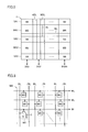
- FIG. 10 is a circuit block diagram showing a principal portion of a conventional dynamic random access memory (hereinafter DRAM).
- the DRAM includes a plurality of memory cells MC arranged in rows and columns, a word line WL provided correspondingly to each row, a pair of bit lines BL and /BL provided correspondingly to each column, and a pair of write data lines WDL and /WDL.
- the DRAM further includes a write column select gate 50 , a sense amplifier 55 and an equalizer 60 that are provided correspondingly to each column.
- Write column select gate 50 includes N-channel MOS transistors 51 - 54 .
- N-channel MOS transistors 51 and 52 are connected in series between bit line BL and write data line WDL
- N-channel MOS transistors 53 and 54 are connected in series between bit line /BL and write data line /WDL.
- N-channel MOS transistors 51 and 53 have respective gates connected to a write column select line WCSL and N-channel MOS transistors 52 and 54 have respective gates receiving signal WDE.
- Signal WDE is set to L level (logical low level) for write masking and set to H level (logical high level) in normal operation.
- Sense amplifier 55 includes N-channel MOS transistors 56 and 57 and P-channel MOS transistors 58 and 59 .
- N-channel MOS transistors 56 and 57 are connected respectively between bit lines BL and /BL and a node N 51 , and have respective gates connected respectively to bit lines /BL and BL.
- P-channel MOS transistors 58 and 59 are connected respectively between bit lines BL and/BL and a node N 52 , and have respective gates connected respectively to bit lines /BL and BL.
- Nodes N 51 and N 52 receive sense amplifier activation signals SNL and SPL respectively. In a standby state, sense amplifier activation signals SNL and SPL are each set to potential VCC/2, i.e., a half of a power supply potential VCC.
- sense amplifier activation signals SNL and SPL are set respectively to L and H levels.
- Sense amplifier activation signals SNL and SPL are set to L and H levels respectively to activate sense amplifier 55 which in turn amplifies a minute or considerably small potential difference between corresponding paired bit lines BL and /BL up to power supply potential VCC.
- FIG. 11 is a timing chart illustrating a write operation of the DRAM shown in FIG. 10 .
- word line WL is set to the non-selection level, L level, to inactivate memory cell MC.
- Write column select line WCSL is also set to the non-selection level, L level, to make write column select gate 50 nonconductive.
- Equalizer 60 is activated to precharge paired bit lines BL and /BL to precharge potential VCC/2.
- Sense amplifier activation signals SPL and SNL are set to the immediate level VCC/2 to inactivate sense amplifier 55 .
- signal WDE is set to H level.
- active command ACT and row address signal RA are provided, equalizer 60 is inactivated, and word line WL of a row according to row address signal RA is raised to the selection level, H level.
- Word line WL is thus set to H level to activate each memory cell MC corresponding to that word line WL.
- a minute potential difference of a polarity according to data stored in memory cell MC is generated between paired bit lines BL and /BL.
- sense amplifier activation signals SPL and SNL are set to H and L levels respectively to activate sense amplifier 55 . Accordingly, the potential difference between paired bit lines BL and /BL is amplified to power supply potential VCC.
- write command WRT and column address signal CA are provided.
- Write column select line WCSL of a column according to column address signal CA is raised to the selection level, H level, to make write column select gate 50 of that column conductive. Accordingly, paired bit lines BL and /BL of that column and paired write data lines WDL and /WDL are coupled.
- write data lines WDL and /WDL are set respectively at L and H levels for example according to a write data signal. Then, the levels of respective bit lines BL and /BL of the selected column are converted to the levels of respective write data lines WDL and /WDL. The levels of bit lines BL and /BL of any non-selected column are maintained. After a predetermined time has passed, write column select line WCSL is lowered to the non-selection level, L level.
- precharge command PRE is provided.
- Word line WL is lowered to the non-selection level, L level, to inactivate memory cell MC.
- Sense amplifier activation signals SPL and SNL are set to the intermediate level, VCC/2, to inactivate sense amplifier 55 .
- Equalizer 60 is activated and paired bit lines BL and /BL are set to bit line precharge potential VBL. In this way, the data signal is written.
- FIG. 12 is a circuit block diagram showing a principal portion of another conventional DRAM.
- this DRAM differs from the DRAM in FIG. 10 in that the former includes a write column select gate 61 instead of write column select gate 50 .
- Write column select gate 61 includes N-channel MOS transistors 62 - 65 .
- N-channel MOS transistors 62 and 63 are connected in series between bit line BL and a line of a ground potential GND.
- N-channel MOS transistors 64 and 65 are connected in series between bit line /BL and the line of ground potential GND.
- N-channel MOS transistors 62 and 64 have respective gates both connected to write column select line WCSL, and N-channel MOS transistors 63 and 65 have respective gates connected respectively to write data lines /WDL and WDL.
- N-channel MOS transistors 62 and 64 When write column select line WCSL is raised to the selection level, H level, N-channel MOS transistors 62 and 64 are turned on. When write data lines WDL and /WDL have H and L levels respectively, N-channel MOS transistor 65 is turned on while N-channel MOS transistor 63 is turned off. Then, bit line /BL is lowered to L level, and sense amplifier 55 raises bit line BL to H level. When write data lines WDL and /WDL have L and H levels respectively, N-channel MOS transistor 63 is turned on while N-channel MOS transistor 65 is turned off. Then, bit line BL is lowered to L level and sense amplifier 55 raises bit line /BL to H level. Except for the above-described details, the DRAM shown in FIG. 12 has the same structure and operation as those of the DRAM shown in FIG. 10 and description thereof is not repeated here.
- SRAM static random access memory
- DRAM dynamic random access memory
- One object of the present invention is thus to provide a semiconductor memory device to which enhanced-speed random access is possible.
- a semiconductor memory device includes: a memory block including a plurality of memory cells, a plurality of word lines, and a plurality of pairs of bit lines; a sense amplifier provided correspondingly to each pair of bit lines and activated in response to application of a first drive potential to a first node to amplify a potential difference generated between the bit lines of the corresponding bit line pair; a row decoder selecting one of the word lines according to a row address signal to activate each memory cell corresponding to the selected word line; a column decoder selecting one of the pairs of bit lines according to a column address signal; a pair of write data lines provided commonly to the pairs of bit lines; a write circuit, according to a write data signal, setting one of first and second write data lines included in the pair of write data lines to a first potential and setting the other of the first and second write data lines to a second potential; and a write column select gate transmitting, in write operation, the data signal on the pair of write data lines to the pair of bit lines selected by the column
- the write column select gate includes first and second transistors provided correspondingly to each pair of bit lines, having respective gate electrodes connected to the first and second write data lines respectively and having respective first electrodes both connected to the first node, and third and fourth transistors provided correspondingly to each pair of bit lines, having respective first electrodes connected to respective second electrodes of the first and second transistors and having respective second electrodes connected respectively to first and second bit lines of the corresponding pair of bit lines, the third and fourth transistors being rendered conductive, in the write operation, in response to selection of the corresponding pair of bit lines by the column decoder.
- the sense amplifier never operates unless a drive potential is applied to a predetermined node.
- the column decoder and the write circuit are then activated prior to activation of the sense amplifier so as to allow a data signal to be written into the sense amplifier simultaneously with sensing and amplification of memory cell data, which enhances the random access rate.
- the first and second transistors are provided commonly to the pairs of bit lines.
- the required number of the first and second transistors is thus reduced and the load capacitance of the write circuit accordingly decreases, which provides speedup of write operation.
- the semiconductor memory device further includes a write control circuit activating, in response to a write command signal, the row decoder, the column decoder and the write circuit and thereafter applying the first drive potential to the first node to activate the sense amplifier.
- the write command can thus be issued simply since only one write command signal may be provided.
- the semiconductor memory device further includes a precharge circuit provided correspondingly to each pair of bit lines for precharging the corresponding pair of bit lines to a predetermined potential.
- the write control circuit inactivates, after the write operation is completed, the row decoder, the column decoder, the write circuit and the sense amplifier, and activates the precharge circuit. Only one write command signal is necessary for the process up to precharging and thus the operation of issuing write command is further simplified.
- the sense amplifier includes fifth and sixth transistors of N-channel type, connected respectively between the first and second bit lines and the first node, and having respective gate electrodes connected respectively to the second and first bit lines, and seventh and eighth transistors of P-channel type connected respectively between the first and second bit lines and a second node and having respective gate electrodes connected respectively to the second and first bit lines.
- the sense amplifier is activated in response to application of the first drive potential to the first node and application of the second drive potential to the second node. Then, the sense amplifier can readily be formed.
- FIG. 1 is a block diagram showing an entire structure of a DRAM according to a first embodiment of the present invention.
- FIG. 2 is a block diagram showing a configuration of a memory mat shown in FIG. 1 .
- FIG. 3 is a circuit block diagram showing a configuration of a memory block shown in FIG. 2 .
- FIG. 4 is a circuit block diagram showing a configuration of a sense block in FIG. 2 .
- FIG. 5 is a circuit block diagram showing a configuration of a sense amplifier and input/output control circuit 8 shown in FIG. 4 .
- FIG. 6 is a circuit diagram showing a configuration of an equalizer shown in FIG. 5 .
- FIG. 7 is a timing chart illustrating a write operation of the DRAM shown in FIGS. 1-6.
- FIG. 8 is a block diagram for supplemental description of the DRAM shown in FIG. 1 .
- FIG. 9 is a circuit block diagram showing a principal portion of a DRAM according to a second embodiment of the present invention.
- FIG. 10 is a circuit block diagram showing a principal portion of a conventional DRAM.
- FIG. 11 is a timing chart illustrating a write operation of the DRAM shown in FIG. 10 .
- FIG. 12 is a circuit block diagram showing a principal portion of another conventional DRAM.
- FIG. 1 is a block diagram showing an entire structure of a DRAM 1 according to a first embodiment of the present invention.
- DRAM 1 includes a row/column address buffer and clock generator circuit 2 , a row/column decoder circuit 3 , a memory mat 4 and a data input/output circuit 5 .
- simultaneous input/output of 8 k (k is an integer of at least 1) data signals DQ 1 -DQ 8 k is possible.
- one input terminal for write mask signal WM is provided.
- Row/column address buffer and clock generator circuit 2 provides externally supplied row address signals RA 0 -RAm (m is an integer of at least 0) and column address signals CA 0 -CAn (n is an integer of at least 0) to row/column decoder circuit 3 , and further generates read clock signal CLKR and write clock signal CLKW for example according to external control signals /RAS, /CAS and /WE to control the whole of DRAM 1 .
- Memory mat 4 includes a plurality of (three in FIG. 1) sense amplifier bands SA 1 -SA 3 and memory cell arrays MA 1 and MA 2 provided therebetween.
- Memory cell arrays MA 1 and MA 2 include a plurality of memory cells each storing one data signal. These memory cells are divided into groups each containing a predetermined number ( 8 k ) of cells. Each memory cell group is located at a predetermined address determined by row and column addresses.
- row/column decoder circuit 3 designates any address in memory cell arrays MA 1 and MA 2 .
- Sense amplifier bands SA 1 and SA 2 have sense amplifier and input/output control circuits discussed below.
- the sense amplifier and input/output control circuits couple 8 k memory cells addressed by row/column decoder circuit 3 to data input/output circuit 5 .
- Data input/output circuit 5 includes a write driver and read amplifier band 6 as well as input/output buffers 7 .
- Write driver and read amplifier band 6 includes write drivers and read amplifiers.
- Read amplifiers operate synchronously with read clock signal CLKR to provide read data signals Q 1 -Q 8 k from selected 8 k memory cells to input/output buffers 7 .
- Input/output buffers 7 output, in response to external control signal /OE, read data signals Q 1 -Q 8 k from the read amplifiers to external circuitry.
- Write drivers operate synchronously with write clock signal CLKW to write externally supplied write data signals D 1 -D 8 k into selected 8 k memory cells.
- 8 k memory cells include memory cells designated by write mask signals WM 1 -WMk and these designated memory cells have no data written thereto.
- FIG. 2 is a block diagram showing a configuration of memory mat 4 shown in FIG. 1 .
- memory cell arrays MA 1 and MA 2 are each divided into 8 k memory blocks MB corresponding respectively to data signals DQ 1 -DQ 8 k.
- Sense amplifier bands SA 1 -SA 3 are each divided into 8 k sense blocks SB corresponding respectively to data signals DQ 1 -DQ 8 k.
- Memory mat 4 includes 8 k pairs of read data lines RDL and /RDL for reading respective data signals Q 1 -Q 8 k as well as 8 k pairs of write data lines WDL and /WDL for writing respective data signals D 1 -D 8 k.
- Paired read data lines RDL and/RDL and paired write data lines WDL and /WDL are placed to cross corresponding three sense blocks SB and two memory blocks MB. One end of these lines each is connected to write driver and read amplifier band 6 .
- a memory block MB includes a plurality of memory cells MC arranged in rows and columns, a plurality of word lines WL provided correspondingly to respective rows, and a plurality of pairs of bit lines BL and /BL provided correspondingly to respective columns.
- Memory cell MC is a memory cell of the known type including an N-channel MOS transistor Q for access and a capacitor C for storing information.
- Word line WL is driven to the selection level, H level, to activate each memory cell MC of the row corresponding to that word line WL and accordingly allow data to be written/read into/from each memory cell MC.
- one word line WL is driven to the selection level of H level to activate memory cell MC and then one of bit lines BL and /BL of one bit line pair is set to H level while the other of the bit lines is set to L level according to a corresponding write data signal (e.g. D 1 ).
- the bit line potential is thus written into any desired memory cell MC.
- bit line precharge potential VBL VCC/2
- one word line WL is set to the selection level of H level to activate memory cell MC.
- a sense block SB of sense amplifier band SA 2 includes a sense amplifier and input/output control circuits 8 which is provided correspondingly to each odd-numbered pair of bit lines BL and /BL common to the two memory blocks MB and MB.
- Respective sense blocks SB of sense amplifier bands SA 1 and SA 3 each includes a sense amplifier and input/output control circuit 9 provided correspondingly to each even-numbered pair of bit lines BL and /BL of adjacent memory blocks MB.
- sense amplifier and input/output control circuit 8 includes transfer gates 10 and 13 , equalizers 16 and 17 , a sense amplifier 20 , a read column select gate 25 , and a write column select gate 30 .
- Transfer gate 10 includes a pair of N-channel MOS transistors 11 and 12 connected respectively between nodes N 1 and N 2 and corresponding paired bit lines BL and /BL of memory block MB in memory cell array MA 1 , the MOS transistors having respective gates both receiving signal BLIL.
- Transfer gate 13 includes a pair of N-channel MOS transistors 14 and 15 connected respectively between nodes N 1 and N 2 and corresponding paired bit lines BL and /BL of memory block MB of memory cell array MA 2 , the MOS transistors having respective gates both receiving signal BLIR.
- row/column decoder circuit 3 sets, to L level, one of signals BLIL and BLIR, that is signal BLIL, those two N-channel MOS transistors 11 and 12 of transfer gate 10 are turned off to disconnect paired bit lines BL and /BL of memory cell array MA 1 from nodes N 1 and N 2 .
- row/column decoder circuit 3 sets, to L level, one of signals BLIL and BLIR, that is signal BLIR, those two N-channel MOS transistors 14 and 15 of transfer gate 13 are turned off to disconnect paired bit lines BL and /BL in memory cell array MA 2 from nodes N 1 and N 2 .
- Equalizer 16 is connected to paired bit lines BL and /BL in memory cell array MA 1 .
- bit line equalize signal BLEQL is set to the activation level, L level
- equalizer 16 includes P-channel MOS transistors 35 - 37 .
- P-channel MOS transistor 35 is connected between paired bit lines BL and /BL, and P-channel MOS transistors 36 and 37 are connected in series between paired bit lines BL and /BL.
- P-channel MOS transistors 35 - 37 have respective gates receiving bit line equalize signal BLEQL.
- bit line equalize signal BLEQL When row/column decoder circuit 3 sets bit line equalize signal BLEQL to the activation level, L level, P-channel MOS transistors 35 - 37 are turned on to equalize bit lines BL and /BL both to bit line precharge potential VBL. When row/column decoder circuit 3 sets bit line equalize signal BLEQL to the inactivation reveal, H level, P-channel MOS transistors 35 - 37 are turned off to stop equalizing of bit lines BL and /BL
- equalizer 17 is connected to paired bit lines BL and /BL in memory cell array MA 2 .
- bit line equalize signal BLEQR is set to the activation level, L level
- equalizer 17 equalizes corresponding paired bit lines BL and /BL to bit line precharge potential VBL.
- Equalizer 17 is structured similarly to equalizer 16 .
- Sense amplifier 20 is activated when sense amplifier activation signals SNL and SPL are set respectively to L and H levels to amplify a minute potential difference between nodes N 1 and N 2 to power supply potential VCC.
- sense amplifier 20 includes N-channel MOS transistors 21 and 22 and P-channel MOS transistors 23 and 24 .
- N-channel MOS transistors 21 and 22 are connected respectively between nodes N 1 and N 2 and a node N 3 , and have respective gates connected to nodes N 2 and N 1 .
- P-channel MOS transistors 23 and 24 are connected respectively between nodes N 1 and N 2 and a node N 4 , and have respective gates connected to nodes N 2 and N 1 .
- Nodes N 3 and N 4 receive respective sense amplifier activation signals SNL and SPL.
- Sense amplifier activation signals SNL and SPL are generated by row/column decoder circuit 3 , both set to the intermediate level (VCC/2) in a standby mode and set respectively at L level and H level in an active mode
- nodes N 1 -N 4 are all set to the intermediate level VCC/2 to cause all MOS transistors 21 - 24 to be turned off.
- a minute potential difference between paired bit lines BL and /BL is transmitted to nodes N 1 and N 2 while nodes N 3 and N 4 are set respectively to L level and H level.
- MOS transistors 22 and 23 have a resistance value lower than that of MOS transistors 21 and 24 . Then, the potential on node N 1 is raised to power supply potential VCC while the potential on node N 2 is lowered to ground potential GND. If the potential on node N 2 is higher than that on node N 1 , MOS transistors 21 and 24 have a resistance value lower than that of MOS transistors 22 and 23 . Then, the potential on node N 2 is raised to power supply potential VCC while the potential on node N 1 is lowered to ground potential GND.
- Read select gate 25 includes N-channel MOS transistors 26 and 27 .
- N-channel MOS transistors 26 and 27 are connected respectively between nodes N 1 and N 2 and read data lines RDL and /RDL and have respective gates connected to read column select line RCSL of a corresponding column.
- Read column select line RCSL is provided correspondingly to each sense amplifier and input/output control circuit 8 and commonly to 8 k sense blocks SB in sense amplifier band SA 2 .
- row/column decoder circuit 3 sets read column select line RCSL according to column address signals CA 0 -CAn to the selection level, H level, N-channel MOS transistors 26 and 27 of read column select gate 25 of that column are turned on, and accordingly the potentials on nodes N 1 and N 2 are transmitted through N-channel MOS transistors 26 and 27 to read data lines RDL and /RDL.
- Write column select gate 30 includes N-channel MOS transistors 31 - 34 .
- N-channel MOS transistors 31 and 32 are connected in series between nodes N 1 and N 3 and N-channel MOS transistors 33 and 34 are connected in series between nodes N 2 and N 3 .
- N-channel MOS transistors 31 and 33 have respective gates both connected to write column select line WCSL of a corresponding column.
- N-channel MOS transistors 34 and 32 have respective gates connected respectively to write data lines WDL and /WDL.
- Write column select line WCSL is provided correspondingly to each sense amplifier and input/output control circuit 8 and commonly to 8 k sense blocks SB in sense amplifier band SA 2 .
- row/column decoder circuit 3 sets write column select line WCSL according to column address signals CA 0 -CAn to the selection level, H level, N-channel MOS transistors 31 and 33 of write column select gate 30 of that column are turned on. If write data lines WDL and /WDL have H and L levels respectively, one of N-channel MOS transistors 32 and 34 , that is N-channel MOS transistors 34 , is turned on. Accordingly, node N 2 is set to L level and node N 1 is set to H level by sense amplifier 20 . If write data lines WDL and /WDL have L land H levels respectively, one of N-channel MOS transistors 32 and 34 , that is N-channel MOS transistor 32 , is turned on. Accordingly, node N 1 is set to L level and node N 2 is set to H level by sense amplifier 20 .
- Sense amplifier and input/output control circuit 9 in sense amplifier band SA 1 differs from sense amplifier and input/output control circuit 8 in sense amplifier band SA 2 in that the circuit 9 does not include transfer gates 10 and 13 and equalizer 17 for memory cell array MA 2 .
- Sense amplifier and input/output control circuit 9 in sense amplifier band SA 3 differs from sense amplifier and input/output control circuit 8 in sense amplifier band SA 2 in that the circuit 9 does not include transfer gates 10 and 13 and equalizer 16 for memory cell array MA 1 .
- Column select lines RCSL and WCSL are provided separately to sense amplifier band SA 1 and sense amplifier band SA 3 .
- FIG. 7 is a timing chart illustrating a write operation of this DRAM.
- word line WL has the non-selection level, L level, and accordingly memory cell MC is inactivated.
- write column select line WCSL has the non-selection level, L level, and accordingly N-channel MOS transistors 31 and 33 of write column select gate 30 are turned off.
- Equalizers 16 and 17 are activated to precharge paired bit lines BL and /BL to bit line precharge potential VCC/2.
- Sense amplifier activation signals SPL and SNL have the intermediate level VCC/2 to inactivate sense amplifier 20 .
- Signals BLIL and BLIR have H level to render transfer gates 10 and 13 nonconductive, and read column select line RCSL has the non-selection level, L level, and accordingly read column select gate 25 is rendered nonconductive.
- write command WRT row address signals RA 0 -RAm and column address signals CA 0 -CAn are simultaneously provided.
- memory cell array MA 1 is selected according to row address signals RA 0 -RAm.
- signal BLIR is set to L level to render transfer gate 13 nonconductive so that sense amplifier 20 is disconnected from memory cell array MA 2 .
- equalizer 16 is inactivated and word line WL according to row address signals RA 0 -RAm is raised to the selection level, H level. In this way, each memory cell MC for that word line WL is activated to cause a minute potential difference between paired bit lines BL and /BL, the difference being of a polarity corresponding to stored data in that memory cell MC.
- write column select line WCSL of a column according to column address signals CA 0 -CAn is raised to the selection level, H level, and N-channel MOS transistors 31 and 33 of write column select gate 30 for that column are turned on.
- write data lines WDL and /WDL are set in advance to H and L levels respectively for example. Accordingly, bit line BL or bit line /BL of the selected column is lowered to L level.
- sense amplifier activation signals SPL and SNL are set respectively to H and L levels to activate sense amplifier 20 , which amplifies the potential difference between paired bit lines BL and /BL to power supply potential VCC.
- respective levels of bit lines BL and /BL of the selected column are changed into respective levels of write data lines WDL and /WDL.
- Bit lines BL and /BL of a non-selected column have their levels maintained.
- write column select line WCSL is lowered to the non-selection level, L level.
- word line WL is lowered to the non-selection level of L level.
- Memory cell MC is thus inactivated, sense amplifier activation signals SPL and SNL are set to the intermediate level VCC/2 to inactivate sense amplifier 20 .
- Equalizer 16 is activated to precharge bit lines BL and /BL to precharge potential VBL.
- Signal BLIR is set to H level and transfer gate 13 is made conductive. This process thus returns to the standby state.
- read command READ is provided instead of write command WRT, and read column select line RCSL is selected instead of write column select line WCSL.
- a potential difference between paired bit lines BL and /BL of a selected column is amplified by sense amplifier 20 , and this amplified potential difference is supplied through read column select gate 25 to paired read data lines RDL and /RDL.
- a read amplifier compares respective potentials on read data lines RDL and /RDL to output a data signal of a logic level according to that comparison through an input/output buffer to any external circuitry. Except for the details above, the reading operation is similar to the write operation.
- FIG. 8 is a block diagram showing in more detail DRAM 1 in FIG. 1 .
- row/column address buffer and clock generator circuit 2 shown in FIG. 1 includes a row address buffer 2 a, a column address buffer 2 b and a clock generator circuit 2 c, and clock generator circuit 2 c includes a write control circuit 2 d and a read control circuit 2 e.
- Row/column decoder circuit 3 includes a row decoder 3 a and a column decoder 3 b.
- Memory mat 4 includes a memory cell array 4 a and a sense amplifier circuit 4 b.
- Write driver and read amplifier band 6 includes a write driver 6 a and a read amplifier 6 b.
- Input/output buffers 7 include an input buffer 7 a and an output buffer 7 b.
- Row address buffer 2 a provides externally supplied row address signals RA 0 -RAm to row decoder 3 a. According to row address signals RA 0 -RAm from row address buffer 2 a, row decoder 3 a selects one of a plurality of word lines WL in memory cell array 4 a to drive the selected word line WL to the selection level of H level.
- Column address buffer 2 b provides externally supplied column address signals CA 0 -CAn to column decoder 3 b.
- column decoder 3 b selects one of a plurality of write column select lines WCSL according to column address signals CA 0 -CAn from column address buffer 2 b to drive the selected write column select line WCSL to the selection level of H level.
- column decoder 3 b selects one of a plurality of read column select lines RCSL according to column address signals CA 0 -CAn from column address buffer 2 b to drive the selected read column select line RCSL to the selection level of H level.
- input buffer 7 a provides externally supplied write data signal D to write driver 6 a.
- write driver 6 a drives one of write data lines WDL and /WDL (e.g. WDL) to H level while driving the other write data line (/WDL) to L level according to write data signal D from input buffer 7 a.
- write driver 6 a drives both of write data lines WDL and /WDL to L level.
- read amplifier 6 b compares respective potentials on read data lines RDL and /RDL to generate read data signal Q according to the result of comparison.
- Output buffer 7 b outputs read data signal Q generated by read amplifier 6 b in response to activation of output enable signal /OE to L level.
- write control circuit 2 d controls, as shown in FIG. 7, respective predetermined timings of row address buffer 2 a, row decoder 3 a, column address buffer 2 b, column decoder 3 b, write driver 6 a and input buffer 7 a to write write data signal D into a selected memory cell MC.
- read control circuit 2 e controls respective predetermined timings of row address buffer 2 a, row decoder 3 a, column address buffer 2 b, column decoder 3 b, read amplifier 6 b and output buffer 7 b to read data signal Q from a selected memory cell MC.
- respective sources of N-channel MOS transistors 32 and 34 of write column select gate 30 are connected to node N 3 . Then, even if write column select line WCSL and paired write data lines WDL and /WDL are driven before sense amplifier 20 is driven, sense amplifier 20 never malfunctions prematurely until sense amplifier activation signals SNL and SPL are set respectively to L and H levels. Data is read from memory cell MC and sense amplifier 20 starts sensing and amplifying for that data while sense amplifier 20 latches an external data signal. Thus, as shown in FIG.
- write column select line WCSL and paired write data lines WDL and /WDL are driven prior to activation of sense amplifier 20 , which makes it possible to write the external data signal into sense amplifier 20 simultaneously with sensing and amplification of the memory cell data and thus makes it possible to enhance the frequency of random access.
- execution of the write operation requires only the write command WRT.
- the command can thus be issued in a simplified manner compared with the conventional command operation which requires three commands, i.e., active command ACT, write command WRT and precharge command PRE.
- sense amplifier activation signals SNL and SPL are charged to the intermediate level VCC/2
- write column select line WCSL of a selected column is set to H level
- write data lines WDL and /WDL are set respectively to H and L levels.
- bit lines BL and /BL of the selected column have H and L levels respectively.
- MOS transistors 57 and 58 of sense amplifier 55 of the selected column are turned on to set nodes N 51 and N 52 to L and H levels respectively.
- sense amplifier 55 starts its sensing operation before a minute potential difference is read appropriately from memory cell MC onto paired bit lines BL and /BL, which hinders normal sensing and amplifying operation.
- Memory cell data might normally be read by providing nodes N 51 and N 52 separately for each sense amplifier 55 to prevent any sense amplifier 55 of a non-selected column from operating. Actually, however, paired bit lines BL and /BL of a selected column are coupled with paired bit lines BL and /BL of an adjacent column to cause noise on the adjacent pair of bit lines BL and /BL. Then, the normal sensing and amplifying operation is impossible here.
- bit line BL or bit line /BL of the selected column has L level.
- N-channel MOS transistor 57 of the selected column is turned on to set node N 51 to L level.
- sense amplifier 55 starts its sensing operation before a minute potential difference is normally read from memory cell MC onto paired bit lines BL and /BL, which also hinders normal sensing and amplifying operation.
- FIG. 9 is a circuit block diagram showing a principal portion of a DRAM according to a second embodiment of the present invention. As FIG. 9 is compared with FIG. 5, it is found that the DRAM in FIG. 9 differs from the DRAM in FIG. 5 in that the former DRAM includes a write column select gate(s) 30 ′ instead of write column select gate(s) 30 except for one write column select gate 30 among a plurality of (two in FIG. 5) write column select gates 30 .
- Write column select gate 30 ′ lacks N-channel MOS transistors 32 and 34 of write column select gate 30 .
- Write column select gate 30 ′ includes N-channel MOS transistors 31 and 33 having respective sources connected to respective sources of N-channel MOS transistors 31 and 33 of write column select gate 30 .
- the structure and operation of the second embodiment except for the details discussed above are the same as those of the first embodiment and description thereof is not repeated here.
- paired write data lines WDL and /WDL have reduced capacity, which makes it possible to speed up the write operation and reduce the power consumption.
Abstract
Description
Claims (10)
Applications Claiming Priority (2)
| Application Number | Priority Date | Filing Date | Title |
|---|---|---|---|
| JP2001-397190 | 2001-12-27 | ||
| JP2001397190A JP2003196983A (en) | 2001-12-27 | 2001-12-27 | Semiconductor memory |
Publications (2)
| Publication Number | Publication Date |
|---|---|
| US20030123317A1 US20030123317A1 (en) | 2003-07-03 |
| US6674685B2 true US6674685B2 (en) | 2004-01-06 |
Family
ID=19189158
Family Applications (1)
| Application Number | Title | Priority Date | Filing Date |
|---|---|---|---|
| US10/222,840 Expired - Lifetime US6674685B2 (en) | 2001-12-27 | 2002-08-19 | Semiconductor memory device having write column select gate |
Country Status (2)
| Country | Link |
|---|---|
| US (1) | US6674685B2 (en) |
| JP (1) | JP2003196983A (en) |
Cited By (2)
| Publication number | Priority date | Publication date | Assignee | Title |
|---|---|---|---|---|
| US6909664B1 (en) * | 2004-05-20 | 2005-06-21 | Fujitsu Limited | Semiconductor memory device with simplified control of column switches |
| KR20110137192A (en) * | 2010-06-16 | 2011-12-22 | 삼성전자주식회사 | Multi-page program method, non-volatile memory device usign the same, and data storage system including the same |
Families Citing this family (2)
| Publication number | Priority date | Publication date | Assignee | Title |
|---|---|---|---|---|
| KR100780613B1 (en) | 2006-06-30 | 2007-11-29 | 주식회사 하이닉스반도체 | Semiconductor memory device and driving method thereof |
| JP2019102106A (en) * | 2017-11-28 | 2019-06-24 | ルネサスエレクトロニクス株式会社 | Semiconductor device |
Citations (4)
| Publication number | Priority date | Publication date | Assignee | Title |
|---|---|---|---|---|
| JPH08111093A (en) | 1995-10-18 | 1996-04-30 | Sanyo Electric Co Ltd | Semiconductor storage device |
| JPH08147975A (en) | 1994-11-14 | 1996-06-07 | Sony Corp | Semiconductor memory circuit |
| US6278653B1 (en) * | 2000-06-16 | 2001-08-21 | United Memories, Inc. | Reduced skew timing scheme for write circuitry used in memory circuits |
| US6330202B1 (en) | 1999-11-12 | 2001-12-11 | Mitsubishi Denki Kabushiki Kaisha | Semiconductor memory device having write data line |
-
2001
- 2001-12-27 JP JP2001397190A patent/JP2003196983A/en not_active Withdrawn
-
2002
- 2002-08-19 US US10/222,840 patent/US6674685B2/en not_active Expired - Lifetime
Patent Citations (5)
| Publication number | Priority date | Publication date | Assignee | Title |
|---|---|---|---|---|
| JPH08147975A (en) | 1994-11-14 | 1996-06-07 | Sony Corp | Semiconductor memory circuit |
| JPH08111093A (en) | 1995-10-18 | 1996-04-30 | Sanyo Electric Co Ltd | Semiconductor storage device |
| US6330202B1 (en) | 1999-11-12 | 2001-12-11 | Mitsubishi Denki Kabushiki Kaisha | Semiconductor memory device having write data line |
| US6278653B1 (en) * | 2000-06-16 | 2001-08-21 | United Memories, Inc. | Reduced skew timing scheme for write circuitry used in memory circuits |
| US6339541B1 (en) * | 2000-06-16 | 2002-01-15 | United Memories, Inc. | Architecture for high speed memory circuit having a relatively large number of internal data lines |
Non-Patent Citations (2)
| Title |
|---|
| Y. Agata, et al, "An 8ns Random Cycle Embedded RAM Macro With Dual-Port Interleaved DRAM Architecture (D<2>RAM)" Digest of Technical Papers of 2000 IEEE International Solid-State Circuits Conference, Feb. 9, 2000, pp. 392-393. |
| Y. Agata, et al, "An 8ns Random Cycle Embedded RAM Macro With Dual-Port Interleaved DRAM Architecture (D2RAM)" Digest of Technical Papers of 2000 IEEE International Solid-State Circuits Conference, Feb. 9, 2000, pp. 392-393. |
Cited By (6)
| Publication number | Priority date | Publication date | Assignee | Title |
|---|---|---|---|---|
| US6909664B1 (en) * | 2004-05-20 | 2005-06-21 | Fujitsu Limited | Semiconductor memory device with simplified control of column switches |
| KR20110137192A (en) * | 2010-06-16 | 2011-12-22 | 삼성전자주식회사 | Multi-page program method, non-volatile memory device usign the same, and data storage system including the same |
| US20110310673A1 (en) * | 2010-06-16 | 2011-12-22 | Samsung Electronics Co., Ltd | Multi-page program method, non-volatile memory device using the same, and data storage system including the same |
| US8717817B2 (en) * | 2010-06-16 | 2014-05-06 | Samsung Electronics Co., Ltd. | Method for multi-page programming a non-volatile memory device by simultaneously activating a plurality of selection lines based on programmed data |
| US8873290B2 (en) | 2010-06-16 | 2014-10-28 | Samsung Electronics Co., Ltd. | Non-volatile memory device capable of multi-page programming by simultaneously activating a plurality of selection lines based on programmed data |
| KR101662821B1 (en) | 2010-06-16 | 2016-10-05 | 삼성전자주식회사 | Multi-page program method, non-volatile memory device usign the same, and data storage system including the same |
Also Published As
| Publication number | Publication date |
|---|---|
| US20030123317A1 (en) | 2003-07-03 |
| JP2003196983A (en) | 2003-07-11 |
Similar Documents
| Publication | Publication Date | Title |
|---|---|---|
| KR100342314B1 (en) | Semiconductor memory device | |
| US5220527A (en) | Dynamic type semiconductor memory device | |
| KR20040038449A (en) | Semiconductor memory device having hierachical data input/output line and method for precharging therefor | |
| EP1039471B1 (en) | Semiconductor integrated circuit and semiconductor memory device including overdriving sense amplifier | |
| US6400629B1 (en) | System and method for early write to memory by holding bitline at fixed potential | |
| US6542426B2 (en) | Cell data protection circuit in semiconductor memory device and method of driving refresh mode | |
| US5555523A (en) | Semiconductor memory device | |
| US5719814A (en) | Semiconductor memory device capable of storing high potential level of data | |
| US5881006A (en) | Semiconductor memory device | |
| US6320806B1 (en) | Input/output line precharge circuit and semiconductor memory device adopting the same | |
| US5642326A (en) | Dynamic memory | |
| CN115810372A (en) | Apparatus and method for single-ended sense amplifier | |
| US6301175B1 (en) | Memory device with single-ended sensing and low voltage pre-charge | |
| US20110176379A1 (en) | Semiconductor memory device having memory cell array of open bit line type and control method thereof | |
| US6292417B1 (en) | Memory device with reduced bit line pre-charge voltage | |
| US6304494B1 (en) | Semiconductor device with decreased power consumption | |
| US7012831B2 (en) | Semiconductor memory device | |
| US5877990A (en) | Semiconductor memory device and method | |
| US6330202B1 (en) | Semiconductor memory device having write data line | |
| US6166977A (en) | Address controlled sense amplifier overdrive timing for semiconductor memory device | |
| JP2718577B2 (en) | Dynamic RAM | |
| US5481496A (en) | Semiconductor memory device and method of data transfer therefor | |
| US6674685B2 (en) | Semiconductor memory device having write column select gate | |
| JP2004234810A (en) | Semiconductor memory | |
| US6728122B2 (en) | Semiconductor memory device capable of rewriting data signal |
Legal Events
| Date | Code | Title | Description |
|---|---|---|---|
| AS | Assignment |
Owner name: MITSUBISHI DENKI KABUSHIKI KAISHA, JAPAN Free format text: ASSIGNMENT OF ASSIGNORS INTEREST;ASSIGNOR:FUJINO, TAKESHI;REEL/FRAME:013226/0222 Effective date: 20020701 |
|
| AS | Assignment |
Owner name: RENESAS TECHNOLOGY CORP., JAPAN Free format text: ASSIGNMENT OF ASSIGNORS INTEREST;ASSIGNOR:MITSUBISHI DENKI KABUSHIKI KAISHA;REEL/FRAME:014502/0289 Effective date: 20030908 |
|
| FEPP | Fee payment procedure |
Free format text: PAYOR NUMBER ASSIGNED (ORIGINAL EVENT CODE: ASPN); ENTITY STATUS OF PATENT OWNER: LARGE ENTITY |
|
| STCF | Information on status: patent grant |
Free format text: PATENTED CASE |
|
| AS | Assignment |
Owner name: RENESAS TECHNOLOGY CORP., JAPAN Free format text: ASSIGNMENT OF ASSIGNORS INTEREST;ASSIGNOR:MITSUBISHI DENKI KABUSHIKI KAISHA;REEL/FRAME:015185/0122 Effective date: 20030908 |
|
| FPAY | Fee payment |
Year of fee payment: 4 |
|
| AS | Assignment |
Owner name: RENESAS ELECTRONICS CORPORATION, JAPAN Free format text: CHANGE OF NAME;ASSIGNOR:RENESAS TECHNOLOGY CORP.;REEL/FRAME:024973/0001 Effective date: 20100401 |
|
| FPAY | Fee payment |
Year of fee payment: 8 |
|
| FPAY | Fee payment |
Year of fee payment: 12 |
|
| AS | Assignment |
Owner name: RENESAS ELECTRONICS CORPORATION, JAPAN Free format text: CHANGE OF ADDRESS;ASSIGNOR:RENESAS ELECTRONICS CORPORATION;REEL/FRAME:044928/0001 Effective date: 20150806 |