US6661072B1 - Piezoelectric ceramic transistor - Google Patents

Piezoelectric ceramic transistor Download PDF

Info

Publication number
US6661072B1
US6661072B1 US10/158,870 US15887002A US6661072B1 US 6661072 B1 US6661072 B1 US 6661072B1 US 15887002 A US15887002 A US 15887002A US 6661072 B1 US6661072 B1 US 6661072B1
Authority
US
United States
Prior art keywords
piezoelectric ceramic
capacitor
voltage transformer
transistor
transformer
Prior art date
Legal status (The legal status is an assumption and is not a legal conclusion. Google has not performed a legal analysis and makes no representation as to the accuracy of the status listed.)
Expired - Fee Related
Application number
US10/158,870
Other versions
US20030222323A1 (en
Inventor
Eddie Cheng
Current Assignee (The listed assignees may be inaccurate. Google has not performed a legal analysis and makes no representation or warranty as to the accuracy of the list.)
Shin Jiuh Corp
Original Assignee
Shin Jiuh Corp
Priority date (The priority date is an assumption and is not a legal conclusion. Google has not performed a legal analysis and makes no representation as to the accuracy of the date listed.)
Filing date
Publication date
Application filed by Shin Jiuh Corp filed Critical Shin Jiuh Corp
Priority to US10/158,870 priority Critical patent/US6661072B1/en
Assigned to SHIN JIUH CORP. reassignment SHIN JIUH CORP. ASSIGNMENT OF ASSIGNORS INTEREST (SEE DOCUMENT FOR DETAILS). Assignors: CHENG, EDDIE
Publication of US20030222323A1 publication Critical patent/US20030222323A1/en
Application granted granted Critical
Publication of US6661072B1 publication Critical patent/US6661072B1/en
Assigned to ZIPPY TECHNOLOGY CORP. reassignment ZIPPY TECHNOLOGY CORP. CORRECTION TO ASSIGMENT PREVIOUSLY RECORDED AT REEL 12953, FRAME 509 Assignors: CHENG, EDDIE
Anticipated expiration legal-status Critical
Expired - Fee Related legal-status Critical Current

Links

Images

Classifications

    • HELECTRICITY
    • H10SEMICONDUCTOR DEVICES; ELECTRIC SOLID-STATE DEVICES NOT OTHERWISE PROVIDED FOR
    • H10NELECTRIC SOLID-STATE DEVICES NOT OTHERWISE PROVIDED FOR
    • H10N30/00Piezoelectric or electrostrictive devices
    • H10N30/80Constructional details
    • H10N30/802Drive or control circuitry or methods for piezoelectric or electrostrictive devices not otherwise provided for
    • H10N30/804Drive or control circuitry or methods for piezoelectric or electrostrictive devices not otherwise provided for for piezoelectric transformers
    • HELECTRICITY
    • H05ELECTRIC TECHNIQUES NOT OTHERWISE PROVIDED FOR
    • H05BELECTRIC HEATING; ELECTRIC LIGHT SOURCES NOT OTHERWISE PROVIDED FOR; CIRCUIT ARRANGEMENTS FOR ELECTRIC LIGHT SOURCES, IN GENERAL
    • H05B41/00Circuit arrangements or apparatus for igniting or operating discharge lamps
    • H05B41/14Circuit arrangements
    • H05B41/26Circuit arrangements in which the lamp is fed by power derived from dc by means of a converter, e.g. by high-voltage dc
    • H05B41/28Circuit arrangements in which the lamp is fed by power derived from dc by means of a converter, e.g. by high-voltage dc using static converters
    • H05B41/282Circuit arrangements in which the lamp is fed by power derived from dc by means of a converter, e.g. by high-voltage dc using static converters with semiconductor devices
    • H05B41/2821Circuit arrangements in which the lamp is fed by power derived from dc by means of a converter, e.g. by high-voltage dc using static converters with semiconductor devices by means of a single-switch converter or a parallel push-pull converter in the final stage
    • H05B41/2822Circuit arrangements in which the lamp is fed by power derived from dc by means of a converter, e.g. by high-voltage dc using static converters with semiconductor devices by means of a single-switch converter or a parallel push-pull converter in the final stage using specially adapted components in the load circuit, e.g. feed-back transformers, piezoelectric transformers; using specially adapted load circuit configurations

Definitions

  • the invention relates to a piezoelectric ceramic transistor. More particularly, the invention provides an electric element that is suitable for use in piezoelectric converter device, and can increase electric power.
  • present driving devices for driving cold cathode fluorescent lamp comprises a driving device and a CCFL driven by the driving device.
  • the driving device comprises a power supply unit 1 , a pulse width modulation (PWM) control unit 2 , a driving unit 3 , and a piezoelectric ceramic voltage transformer 4 ′.
  • the CCFL 7 connects to the PWM 2 through a current feedback 5 and the piezoelectric ceramic voltage transformer 4 ′ connects to the PWM 2 through the voltage feedback 6 .
  • the driving unit 3 immediately drives the piezoelectric ceramic voltage transformer 4 ′ that in turn drives the illumination of the CCFL 7 via piezoelectric ceramic reverse effect.
  • the PWM control unit 2 then detects the average output current intensity of the CCFL 7 through current feedback 5 to output a resonance frequency.
  • the resonance frequency via the control unit 3 and the piezoelectric ceramic voltage transformer 4 ′ can control the average current of the CCFL 7 .
  • the light source generated from the CCFL 7 is projected on the semi-transparent back panel to illuminate the back panel and match the display frame of the LCD screen. Because the illumination of the CCFL 7 via driving of the above driving device is limited or uniform, several CCFL 7 are therefore needed to obtain a uniform back panel illumination of the LCD screen. As a result, the fabrication cost is increased, and the fabrication process further is not easily achieved.
  • the above capacitor thereby forms a bypass capacitor that increases the power and prevents a loss due to feedback so that vibrations of the piezoelectric ceramic voltage transformer are compensated.
  • the above connection scheme is achieved by either serial connecting a capacitor between a power output of the transformer and a load terminal, or parallel connecting a first capacitor to a power input of the transformer while a second capacitor is series connected between a power output of the transformer and the load terminal to obtain an increased power and thereby increasing the load current.
  • Another object of the invention is to provide a piezoelectric ceramic transistor that is formed either via the connection of traditionally known electric elements or via semiconductor packaging into a single element.
  • Another object of the invention is to provide a piezoelectric ceramic transistor that can reduce the number of CCFL mounted to the LCD screen so that the fabrication is facilitated and the fabrication cost reduced.
  • Another object of the invention is to provide a piezoelectric ceramic transistor that can allow CCFL with higher power or of longer length, or CCFL drive with lower driving voltage.
  • FIG. 1 is a block diagram illustrating a background light source driving circuit of LCD screen
  • FIG. 2 illustrates a corresponding circuit of the block diagram of FIG. 1
  • FIG. 3 is a block diagram of an implementation circuit according to an embodiment of the invention.
  • FIG. 4 is a circuit diagram corresponding to the block diagram of FIG. 3;
  • FIG. 5 is a block diagram illustrating another embodiment of the invention.
  • FIG. 6 is a block diagram still illustrating another embodiment of the invention.
  • FIG. 3 and FIG. 4 two block diagrams schematically illustrate an implementation circuit according to an embodiment of the invention.
  • the piezoelectric ceramic transistor of the invention is principally formed via serial connecting a capacitor to an input terminal of a single-layered or multi-stacked layers piezoelectric ceramic voltage transformer (piezoelectric layer).
  • a LCD screen driving device is illustrated as an example of embodiment of the invention.
  • This driving device comprises a power supply unit 1 , a pulse width modulation (PWM) control unit 2 , a driving unit 3 , and a piezoelectric ceramic transistor 4 . Constructed as above, the driving device is used to drive a cold cathode fluorescent lamp (CCFL) 7 that produces a light source for the back-light of the LCD.
  • the power supply unit 1 provides power necessary for the operation of all the units of the driving device.
  • the PWM control unit 4 is connected to an input terminal of the driving unit 3 , and respectively receives a current feedback 5 from the CCFL 7 and a voltage feedback 6 from the piezoelectric ceramic transistor 4 . From the current feedback 5 and according to the average current intensity detected from the output of the CCFL 7 , the PWM control unit 4 adequately controls the average current of the CCFL 7 .
  • the driving unit 3 has an input connected to the PWM control unit 2 , and receives a resonance frequency outputted from the PWM control unit 2 .
  • the piezoelectric ceramic transistor 4 is formed by a capacitor 42 parallel connected to an input terminal of a piezoelectric ceramic transformer 41 .
  • the capacitor 42 hence forms a bypass capacitor, which allows to obtain a higher power.
  • the capacitor 42 can prevent loss due to feedback, and contributes to compensate the vibration of the piezoelectric ceramic transistor 41 .
  • the driving unit 3 When the driving device is turned on, the driving unit 3 immediately drives the piezoelectric ceramic transistor 4 that in turn drives the CCFL 7 for illumination operation. At this moment, the PWM control unit 2 measures the average current intensity outputted from the CCFL 7 through the current feedback 5 , and outputs a resonance frequency. The resonance frequency is delivered to the driving unit 3 and piezoelectric ceramic transistor 4 to control the average current of the CCFL 7 .
  • connection of the capacitor to the single-layered or multi-stacked layers piezoelectric ceramic transformer are illustrated hereafter.
  • the addition of the capacitor of 0.127 uf can turn on the single-layered piezoelectric ceramic transformer.
  • the problem related to the requisite use of a step-up voltage transformer to first step-up voltage before driving the single-layered piezoelectric ceramic transformer can be thereby improved.
  • the fabrication process hence is facilitated, and the fabrication cost is reduced.
  • tube voltage (RMS) acV 500V
  • tube current (AVG) mAacI 6.86 mA
  • the addition of the capacitor of 0.1 uf can turn on the multi-stacked layers piezoelectric ceramic transformer.
  • FIG. 5 illustrates another embodiment of the invention. As illustrated, besides parallel connecting the capacitor 42 to the input terminal of the transformer 41 , it can be also envisaged to serial connect a capacitor 42 ′ between the output terminal of the transformer 41 and the load (CCFL) 7 to magnify the outputted voltage and, thereby, increase the power.
  • CCFL load
  • FIG. 6 still illustrates another variant embodiment of the invention.
  • the capacitor 42 can be parallel connected to the input terminal of the transformer 41 while being also serial connected between the output terminal of the transformer 41 and the load (CCFL) 7 to magnify the outputted voltage and, thereby, increase the power.
  • CCFL load
  • capacitors 100 pF, 68 nF
  • tube current (AVG) mAacI 8.25 mA.
  • tube current (AVG) mAacI 10.83 mA.
  • the lamp current outputted can be increased via either serial connecting a capacitor to the output terminal of the transformer, or serial connecting a first capacitor to the output of the transformer and simultaneously parallel connecting a second capacitor to the input terminal of the transformer.
  • the invention as described above is advantageous allowing the reduction of the number of lamps 7 mounted to the LCD screen.
  • the corresponding input voltage of the driving device can be also reduced.
  • the number of electric components can be also reduced.
  • the fabrication cost is reduced, and the fabrication process is simpler.
  • the invention is also advantageous allowing a single piezoelectric ceramic transistor 4 element to be formed from the piezoelectric ceramic transformer 41 and the capacitor 42 , 42 ′ via semiconductor packaging process.
  • the piezoelectric ceramic transformer 41 and the capacitor 42 can be connected via traditional electric elements.

Abstract

A piezoelectric ceramic transistor is formed from a single-layered or multi-stacked layers piezoelectric ceramic voltage transformer and a capacitor, the capacitor being series connected to an input terminal of the piezoelectric ceramic voltage transformer to prevent electric power and prevent loss due to feedback, thereby compensating and increasing vibrations of the piezoelectric ceramic voltage transformer. Alternatively, the above connection scheme is achieved by either serial connecting a capacitor between a power output of the transformer and a load terminal, or parallel connecting a first capacitor to a power input of the transformer while a second capacitor is series connected between a power output of the transformer and the load terminal to obtain an increased power and thereby increasing the load current.

Description

FIELD OF THE INVENTION
The invention relates to a piezoelectric ceramic transistor. More particularly, the invention provides an electric element that is suitable for use in piezoelectric converter device, and can increase electric power.
BACKGROUND OF THE INVENTION
As shown in the schematic views of FIG. 1 and FIG. 2, present driving devices for driving cold cathode fluorescent lamp (CCFL) comprises a driving device and a CCFL driven by the driving device. The driving device comprises a power supply unit 1, a pulse width modulation (PWM) control unit 2, a driving unit 3, and a piezoelectric ceramic voltage transformer 4′. The CCFL 7 connects to the PWM 2 through a current feedback 5 and the piezoelectric ceramic voltage transformer 4′ connects to the PWM 2 through the voltage feedback 6. When this driving device is turned on and inputs a voltage, the driving unit 3 immediately drives the piezoelectric ceramic voltage transformer 4′ that in turn drives the illumination of the CCFL 7 via piezoelectric ceramic reverse effect. The PWM control unit 2 then detects the average output current intensity of the CCFL 7 through current feedback 5 to output a resonance frequency. The resonance frequency via the control unit 3and the piezoelectric ceramic voltage transformer 4′ can control the average current of the CCFL 7. Hence, the light source generated from the CCFL 7 is projected on the semi-transparent back panel to illuminate the back panel and match the display frame of the LCD screen. Because the illumination of the CCFL 7 via driving of the above driving device is limited or uniform, several CCFL 7 are therefore needed to obtain a uniform back panel illumination of the LCD screen. As a result, the fabrication cost is increased, and the fabrication process further is not easily achieved.
SUMMARY OF THE INVENTION
It is therefore an object of the invention to provide a piezoelectric ceramic transistor that can overcome the above problems by being fabricated from a single-layered or multi-stacked layers piezoelectric ceramic voltage transformer that has an input terminal series connected to a capacitor. The above capacitor thereby forms a bypass capacitor that increases the power and prevents a loss due to feedback so that vibrations of the piezoelectric ceramic voltage transformer are compensated. Alternatively, the above connection scheme is achieved by either serial connecting a capacitor between a power output of the transformer and a load terminal, or parallel connecting a first capacitor to a power input of the transformer while a second capacitor is series connected between a power output of the transformer and the load terminal to obtain an increased power and thereby increasing the load current.
Another object of the invention is to provide a piezoelectric ceramic transistor that is formed either via the connection of traditionally known electric elements or via semiconductor packaging into a single element.
Furthermore, another object of the invention is to provide a piezoelectric ceramic transistor that can reduce the number of CCFL mounted to the LCD screen so that the fabrication is facilitated and the fabrication cost reduced.
Still, another object of the invention is to provide a piezoelectric ceramic transistor that can allow CCFL with higher power or of longer length, or CCFL drive with lower driving voltage.
To provide a further understanding of the invention, the following detailed description illustrates embodiments and examples of the invention, this detailed description being provided only for illustration of the invention.
BRIEF DESCRIPTION OF THE DRAWINGS
The drawings included herein provide a further understanding of the invention. A brief introduction of the drawings is as follows:
FIG. 1 is a block diagram illustrating a background light source driving circuit of LCD screen;
FIG. 2 illustrates a corresponding circuit of the block diagram of FIG. 1;
FIG. 3 is a block diagram of an implementation circuit according to an embodiment of the invention;
FIG. 4 is a circuit diagram corresponding to the block diagram of FIG. 3;
FIG. 5 is a block diagram illustrating another embodiment of the invention;
FIG. 6 is a block diagram still illustrating another embodiment of the invention;
DETAILED DESCRIPTION OF THE EMBODIMENTS
Wherever possible in the following description, like reference numerals will refer to like elements and parts unless otherwise illustrated.
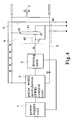
Referring to FIG. 3 and FIG. 4, two block diagrams schematically illustrate an implementation circuit according to an embodiment of the invention. As illustrated, the piezoelectric ceramic transistor of the invention is principally formed via serial connecting a capacitor to an input terminal of a single-layered or multi-stacked layers piezoelectric ceramic voltage transformer (piezoelectric layer). A LCD screen driving device is illustrated as an example of embodiment of the invention. This driving device comprises a power supply unit 1, a pulse width modulation (PWM) control unit 2, a driving unit 3, and a piezoelectric ceramic transistor 4. Constructed as above, the driving device is used to drive a cold cathode fluorescent lamp (CCFL) 7 that produces a light source for the back-light of the LCD. The power supply unit 1 provides power necessary for the operation of all the units of the driving device.
The PWM control unit 4 is connected to an input terminal of the driving unit 3, and respectively receives a current feedback 5 from the CCFL 7 and a voltage feedback 6 from the piezoelectric ceramic transistor 4. From the current feedback 5 and according to the average current intensity detected from the output of the CCFL 7, the PWM control unit 4 adequately controls the average current of the CCFL 7.
The driving unit 3 has an input connected to the PWM control unit 2, and receives a resonance frequency outputted from the PWM control unit 2.
The piezoelectric ceramic transistor 4 is formed by a capacitor 42 parallel connected to an input terminal of a piezoelectric ceramic transformer 41. The capacitor 42 hence forms a bypass capacitor, which allows to obtain a higher power. The capacitor 42 can prevent loss due to feedback, and contributes to compensate the vibration of the piezoelectric ceramic transistor 41.
When the driving device is turned on, the driving unit 3 immediately drives the piezoelectric ceramic transistor 4 that in turn drives the CCFL 7 for illumination operation. At this moment, the PWM control unit 2 measures the average current intensity outputted from the CCFL 7 through the current feedback 5, and outputs a resonance frequency. The resonance frequency is delivered to the driving unit 3 and piezoelectric ceramic transistor 4 to control the average current of the CCFL 7.
The examples of connection of the capacitor to the single-layered or multi-stacked layers piezoelectric ceramic transformer are illustrated hereafter.
I. Single-layered Piezoelectric Ceramic Transformer
A. Testing Conditions:
1. V(DCV): 14V±5%
2. load: lamp length 220 mm
3. working frequency: 66 KHz 2 KHz
4. light regulation conditions: DCV 0V
5. single-layered piezoelectric ceramic transformer: 48 mm L×8 mm W×1.8 mm t
6. static capacitance of low voltage terminal: 1.25 nf
7. number of layers of input terminal: 1 layer
8. testing temperature: 27±10%
B. Test Results:
Without capacitor: tube voltage (RMS) acV: 30V; tube current (AVG) mAacI: 0 mA;
With capacitor: tube voltage (RMS) acV: 567V; tube current (AVG) mAacI: 6.729 mA.
C. Testing Efficiency:
1. without capacitor
tube voltage (RMS)acV×tube current (AVG)mAacI=P_out(w)
30V×0 mA=0W
input voltage (DCV)×input current (DCI)=P_IN
14V×0.036A=0.5W
2. with parallel capacitor
tube voltage (RMS)acV×tube current (AVG)mAacI=P_out(w)
576V×0.6729 mA=3.81W
input voltage (DCV)×input current (DCI)=P_IN
14V×1.268A=17.72W
As shown in the above test results, the addition of the capacitor of 0.127 uf can turn on the single-layered piezoelectric ceramic transformer. The problem related to the requisite use of a step-up voltage transformer to first step-up voltage before driving the single-layered piezoelectric ceramic transformer can be thereby improved. The fabrication process hence is facilitated, and the fabrication cost is reduced.
II. Multi-stacked Layers Piezoelectric Ceramic Transformer
A. Testing Conditions:
1. V(DCV): 12V±5%
2. load: lamp length 220 mm
3. working frequency: 73.39 KHz 2 KHz
4. light regulation conditions: DCV 0V
5. multi-stacked layers piezoelectric ceramic transformer ±10%: 48 mm L×8 mm W×1.8 mm t
6. static capacitance of low voltage terminal: 82.9 nf
7. number of layers of input terminal: 18 layers
8. testing temperature: 27±10%
B. Test Results:
Without capacitor: tube voltage (RMS) acV: 500V; tube current (AVG) mAacI: 6.86 mA;
With capacitor: tube voltage (RMS) acV: 475V; tube current (AVG) mAacI: 13.186 mA.
C. Testing Efficiency:
1. without capacitor
tube voltage (RMS)acV×tube current (AVG)mAacI=P_out(w)
500V×6.86 mA=3.43W
input voltage (DCV)×input current (DCI)=P_IN
12V×0.378A=4.53W
2. with parallel capacitor
tube voltage (RMS)acV×tube current (AVG)mAacI=P_out(w)
475V×13.186 mA=6.25W
input voltage (DCV)×input current (DCI)=P_IN
12V×0.882A=10.58W
As shown in the above test results, the addition of the capacitor of 0.1 uf can turn on the multi-stacked layers piezoelectric ceramic transformer.
FIG. 5 illustrates another embodiment of the invention. As illustrated, besides parallel connecting the capacitor 42 to the input terminal of the transformer 41, it can be also envisaged to serial connect a capacitor 42′ between the output terminal of the transformer 41 and the load (CCFL) 7 to magnify the outputted voltage and, thereby, increase the power.
FIG. 6 still illustrates another variant embodiment of the invention. As shown, the capacitor 42 can be parallel connected to the input terminal of the transformer 41 while being also serial connected between the output terminal of the transformer 41 and the load (CCFL) 7 to magnify the outputted voltage and, thereby, increase the power.
The following results compare a scheme connection in which the piezoelectric ceramic voltage transformer is not connected to any capacitors and connection schemes in which a capacitor is serial connected between the output terminal and the load terminal, or different capacitors are simultaneously parallel and serial connected between the input terminal and the output terminal of the piezoelectric ceramic voltage transformer
A. Testing Conditions:
1. V(DCV): 1.12V±5%
2. load: lamp length 220 mm×1 unit
3. working frequency: 74 KHz 2 KHz
4. light regulation conditions: DCV 0V
5. single layer piezoelectric ceramic transformer: 42 mm
L×7.4 mm W×3.7 mm t
6. static capacitance of low voltage terminal: 185 nf
7. number of layers of input terminal: 18 layers
8. testing temperature: 27±10%
9. capacitors: 100 pF, 68 nF
B. Test Results:
Without capacitor: tube current (AVG) mAacI: 7.21 mA;
With a capacitor of 100 pF serial connected to the output terminal: tube current (AVG) mAacI: 8.25 mA.
With a capacitor of 100 pF serial connected to the output terminal and a capacitor of 68 nF parallel connected to the input terminal: tube current (AVG) mAacI: 10.83 mA.
From the above results, it is observed that the lamp current outputted can be increased via either serial connecting a capacitor to the output terminal of the transformer, or serial connecting a first capacitor to the output of the transformer and simultaneously parallel connecting a second capacitor to the input terminal of the transformer.
The invention as described above is advantageous allowing the reduction of the number of lamps 7 mounted to the LCD screen. Alternatively, with respect to the same conditions of input and load, the corresponding input voltage of the driving device can be also reduced. Thereby, the number of electric components can be also reduced. By further reducing the volume and number of layers of the piezoelectric transformer, the fabrication cost is reduced, and the fabrication process is simpler.
Furthermore, the invention is also advantageous allowing a single piezoelectric ceramic transistor 4 element to be formed from the piezoelectric ceramic transformer 41 and the capacitor 42, 42′ via semiconductor packaging process. Alternatively, the piezoelectric ceramic transformer 41 and the capacitor 42 can be connected via traditional electric elements.
It should be apparent to those skilled in the art that the above description is only illustrative of specific embodiments and examples of the invention. The invention should therefore cover various modifications and variations made to the herein-described structure and operations of the invention, provided they fall within the scope of the invention as defined in the following appended claims.

Claims (6)

What is claimed is:
1. A piezoelectric ceramic transistor, suitable for use in piezoelectric converter device, comprising a piezoelectric ceramic voltage transformer and a capacitor, the capacitor being parallel connected to an input terminal of the piezoelectric ceramic voltage transformer to form a bypass capacitor, thereby the power is increased and loss due to feedback is prevented so that vibrations of the piezoelectric ceramic voltage transformer are compensated.
2. The transistor of claim 1, wherein the piezoelectric ceramic voltage transformer and the capacitor are connected to each other via traditional electric element to form a piezoelectric ceramic transistor with increased power.
3. The transistor of claim 1, wherein the piezoelectric ceramic voltage transformer and the capacitor are processed via semiconductor packaging to form a single piezoelectric ceramic transistor.
4. The transistor of claim 1, wherein the piezoelectric ceramic transistor provides either a cold cathode fluorescent lamp (CCFL) with higher driving power or a CCFL of longer length.
5. A piezoelectric ceramic transistor, suitable for use in piezoelectric converter device, comprising a piezoelectric ceramic voltage transformer and a capacitor, the capacitor being serial connected between an output terminal of the piezoelectric ceramic voltage transformer and a load terminal, thereby magnifying an output voltage and increasing the power.
6. A piezoelectric ceramic transistor, suitable for use in piezoelectric converter device, comprising a piezoelectric ceramic voltage transformer and at least a first and a second capacitor, wherein the first capacitor being parallel connected to an input terminal of the piezoelectric ceramic voltage transformer and between an output terminal of the piezoelectric ceramic voltage transformer and a load terminal so as to form a bypass capacitor used to increase the power and prevent a loss due to a feedback, thereby compensating vibrations of the piezoelectric ceramic voltage transformer; while the second capacitor being serial connected between the output terminal of the piezoelectric ceramic voltage transformer and the load terminal, thereby respectively increasing an output voltage and the power.
US10/158,870 2002-06-03 2002-06-03 Piezoelectric ceramic transistor Expired - Fee Related US6661072B1 (en)

Priority Applications (1)

Application Number Priority Date Filing Date Title
US10/158,870 US6661072B1 (en) 2002-06-03 2002-06-03 Piezoelectric ceramic transistor

Applications Claiming Priority (1)

Application Number Priority Date Filing Date Title
US10/158,870 US6661072B1 (en) 2002-06-03 2002-06-03 Piezoelectric ceramic transistor

Publications (2)

Publication Number Publication Date
US20030222323A1 US20030222323A1 (en) 2003-12-04
US6661072B1 true US6661072B1 (en) 2003-12-09

Family

ID=29582766

Family Applications (1)

Application Number Title Priority Date Filing Date
US10/158,870 Expired - Fee Related US6661072B1 (en) 2002-06-03 2002-06-03 Piezoelectric ceramic transistor

Country Status (1)

Country Link
US (1) US6661072B1 (en)

Cited By (4)

* Cited by examiner, † Cited by third party
Publication number Priority date Publication date Assignee Title
US20040135555A1 (en) * 2002-10-29 2004-07-15 Stmicroelectronics S.R.L. Device for driving a power transistor of a voltage converter provided with a piezoelectric transformer and corresponding voltage converter
US20060267766A1 (en) * 2005-05-30 2006-11-30 Hynix Semiconductor Inc. RFID device having nonvolatile ferroelectric capacitor
US20070160379A1 (en) * 2005-12-26 2007-07-12 Brother Kogyo Kabushiki Kaisha Electronic device and image forming apparatus
TWI394358B (en) * 2009-06-26 2013-04-21 Midas Wei Trading Co Ltd High power output of the piezoelectric power converter

Citations (2)

* Cited by examiner, † Cited by third party
Publication number Priority date Publication date Assignee Title
US5942835A (en) * 1996-10-24 1999-08-24 Nec Corporation Piezoelectric transformer drive circuit
US6028398A (en) * 1995-08-16 2000-02-22 Matsushita Electric Industrial, Co., Ltd. Cold cathode fluorescent lamp driving apparatus using a piezoelectric transformer

Patent Citations (2)

* Cited by examiner, † Cited by third party
Publication number Priority date Publication date Assignee Title
US6028398A (en) * 1995-08-16 2000-02-22 Matsushita Electric Industrial, Co., Ltd. Cold cathode fluorescent lamp driving apparatus using a piezoelectric transformer
US5942835A (en) * 1996-10-24 1999-08-24 Nec Corporation Piezoelectric transformer drive circuit

Cited By (7)

* Cited by examiner, † Cited by third party
Publication number Priority date Publication date Assignee Title
US20040135555A1 (en) * 2002-10-29 2004-07-15 Stmicroelectronics S.R.L. Device for driving a power transistor of a voltage converter provided with a piezoelectric transformer and corresponding voltage converter
US6885172B2 (en) * 2002-10-29 2005-04-26 Stmicroelectronics S.R.L. Device for driving a power transistor of a voltage converter provided with a piezoelectric transformer and corresponding voltage converter
US20060267766A1 (en) * 2005-05-30 2006-11-30 Hynix Semiconductor Inc. RFID device having nonvolatile ferroelectric capacitor
US7710240B2 (en) * 2005-05-30 2010-05-04 Hynix Semiconductor Inc. RFID device having nonvolatile ferroelectric capacitor
US20070160379A1 (en) * 2005-12-26 2007-07-12 Brother Kogyo Kabushiki Kaisha Electronic device and image forming apparatus
US7877035B2 (en) * 2005-12-26 2011-01-25 Brother Kogyo Kabushiki Kaisha Electronic device and image forming apparatus
TWI394358B (en) * 2009-06-26 2013-04-21 Midas Wei Trading Co Ltd High power output of the piezoelectric power converter

Also Published As

Publication number Publication date
US20030222323A1 (en) 2003-12-04

Similar Documents

Publication Publication Date Title
US7109667B2 (en) Discharge lamp driving apparatus
US7489087B2 (en) Backlight inverter and method of driving same
US7332897B2 (en) DC-DC converter
US7215087B2 (en) Discharge lamp lighting apparatus for lighting multiple discharge lamps
JP2009516923A (en) Device for driving an LED cell
TWI306178B (en) Apparatus of driving light source for display device
US7330360B2 (en) Driving apparatus of display device and DC-DC converter
CN1868110A (en) Power converter
EP1617712B1 (en) Discharge lamp lighting apparatus for lighting multiple discharge lamps
US8120262B2 (en) Driving circuit for multi-lamps
TW201128612A (en) LED backlight circuit for LCD panels
US20060017399A1 (en) Discharge lamp lighting apparatus for lighting multiple discharge lamps
US20110122165A1 (en) Lamp driving circuit having low voltage control, backlight unit, and liquid crystal display using the same
US6597123B1 (en) Inverter for driving EL lamp and liquid crystal display
US6661072B1 (en) Piezoelectric ceramic transistor
KR20040073533A (en) Circuit arrangement for operation of one or more lamps
US7656101B2 (en) Cold cathode tube drive device
JP3101783U (en) Digitally controlled multiple light source drive
US7586269B2 (en) Device for driving light source module
EP2202563A1 (en) Electronic apparatus and backlight unit for the same
KR200293245Y1 (en) Piezoelectric ceramic transistor
US7456587B2 (en) Digital controlled light source driving apparatus
US7872431B2 (en) Digital controlled multi-light driving apparatus
JP3510550B2 (en) Piezo transformer drive circuit
JPH10241884A (en) Cold cathode tube lighting drive unit and liquid crystal backlight cold cathode tube lighting drive unit

Legal Events

Date Code Title Description
AS Assignment

Owner name: SHIN JIUH CORP., TAIWAN

Free format text: ASSIGNMENT OF ASSIGNORS INTEREST;ASSIGNOR:CHENG, EDDIE;REEL/FRAME:012953/0509

Effective date: 20020510

AS Assignment

Owner name: ZIPPY TECHNOLOGY CORP., TAIWAN

Free format text: CORRECTION TO ASSIGMENT PREVIOUSLY RECORDED AT REEL 12953, FRAME 509;ASSIGNOR:CHENG, EDDIE;REEL/FRAME:016862/0056

Effective date: 20050711

FPAY Fee payment

Year of fee payment: 4

REMI Maintenance fee reminder mailed
LAPS Lapse for failure to pay maintenance fees
STCH Information on status: patent discontinuation

Free format text: PATENT EXPIRED DUE TO NONPAYMENT OF MAINTENANCE FEES UNDER 37 CFR 1.362

FP Lapsed due to failure to pay maintenance fee

Effective date: 20111209