US6649988B2 - Semiconductor pressure sensor decreasing creep stress in <110> crystalline axis direction - Google Patents
Semiconductor pressure sensor decreasing creep stress in <110> crystalline axis direction Download PDFInfo
- Publication number
- US6649988B2 US6649988B2 US10/122,377 US12237702A US6649988B2 US 6649988 B2 US6649988 B2 US 6649988B2 US 12237702 A US12237702 A US 12237702A US 6649988 B2 US6649988 B2 US 6649988B2
- Authority
- US
- United States
- Prior art keywords
- sides
- metal wiring
- diaphragm
- pressure sensor
- wiring segments
- Prior art date
- Legal status (The legal status is an assumption and is not a legal conclusion. Google has not performed a legal analysis and makes no representation as to the accuracy of the status listed.)
- Expired - Fee Related
Links
Images


Classifications
-
- G—PHYSICS
- G01—MEASURING; TESTING
- G01L—MEASURING FORCE, STRESS, TORQUE, WORK, MECHANICAL POWER, MECHANICAL EFFICIENCY, OR FLUID PRESSURE
- G01L9/00—Measuring steady of quasi-steady pressure of fluid or fluent solid material by electric or magnetic pressure-sensitive elements; Transmitting or indicating the displacement of mechanical pressure-sensitive elements, used to measure the steady or quasi-steady pressure of a fluid or fluent solid material, by electric or magnetic means
- G01L9/0041—Transmitting or indicating the displacement of flexible diaphragms
- G01L9/0051—Transmitting or indicating the displacement of flexible diaphragms using variations in ohmic resistance
- G01L9/0052—Transmitting or indicating the displacement of flexible diaphragms using variations in ohmic resistance of piezoresistive elements
- G01L9/0054—Transmitting or indicating the displacement of flexible diaphragms using variations in ohmic resistance of piezoresistive elements integral with a semiconducting diaphragm
-
- H—ELECTRICITY
- H10—SEMICONDUCTOR DEVICES; ELECTRIC SOLID-STATE DEVICES NOT OTHERWISE PROVIDED FOR
- H10D—INORGANIC ELECTRIC SEMICONDUCTOR DEVICES
- H10D48/00—Individual devices not covered by groups H10D1/00 - H10D44/00
- H10D48/50—Devices controlled by mechanical forces, e.g. pressure
-
- H—ELECTRICITY
- H10—SEMICONDUCTOR DEVICES; ELECTRIC SOLID-STATE DEVICES NOT OTHERWISE PROVIDED FOR
- H10D—INORGANIC ELECTRIC SEMICONDUCTOR DEVICES
- H10D62/00—Semiconductor bodies, or regions thereof, of devices having potential barriers
- H10D62/40—Crystalline structures
- H10D62/405—Orientations of crystalline planes
Definitions
- the present invention relates to a semiconductor pressure sensor, and specifically to a semiconductor pressure sensor that can detect minute pressure.
- a semiconductor pressure sensor includes a semiconductor substrate, a diaphragm and diffusion gauge resistors.
- the diaphragm is formed in the main surface of the substrate.
- the diffusion gauge resistors are formed by ion implantation and diffusion. Then, a detection signal corresponding to pressure applied to the diaphragm can be generated based on a resistance value change of the diffusion gauge resistors.
- metal wiring is formed on the main surface of the substrate for electrically connecting the diffusion gauge resistors to a component outside of the substrate and for outputting the pressure signal through the diffusion gauge resistors.
- Such a semiconductor pressure sensor is typically made with a substrate having a (110) surface as the main surface (hereinafter referred to as a 110 type substrate), because the influence of thermal stress on the 110 type substrate is smaller than on a substrate having a (100) surface as the main surface (hereinafter referred to a 100 type substrate).
- the metal wiring formed on the thick portion is made by depositing Al (aluminum) or the like, but creep stress generated in the metal wiring is supplied to the diaphragm. Therefore, the stress changes the sensor output.
- the sensor is subjected to high temperature in a bonding process for adhering the sensor to a case.
- the thermal stress of the metal wiring is moderated over several hundred hours. Then, stress generated based on the creep stress in the metal wiring is supplied the diaphragm, and the sensor output fluctuates so that the diaphragm is deformed thereby. Therefore, the sensor output includes an error even if trimming is done to the sensor to adjust the output thereof after the bonding process.
- an intermediate sensor detecting range e.g., 100 kPa
- the problem of the output change by creep stress of the metal wiring is not conspicuous because an offset of the sensor output is small.
- an offset of the sensor output caused by creep stress of the metal wiring may be approximately 1 FS %.
- a semiconductor pressure sensor having a ratio S/d is larger than 100, where an area of the diaphragm 12 is S ⁇ m 2 and a thickness thereof is d ⁇ m. In this constitution, minute pressures as small as 10 kPa can be detected.
- the stress sensitivity of the direction of the ⁇ 110> crystalline axis is much larger than that of the direction of the ⁇ 100> crystalline axis.
- the former is fifty times more sensitive than the latter. That is, a piezo-resistance coefficient of the direction of the ⁇ 110> crystalline axis is larger than that of the direction of the ⁇ 100> crystalline axis. Therefore, the ⁇ 110> crystalline direction is used for pressure detection on the (110) surface.
- diffusion gauge resistors As the direction of the ⁇ 110> crystalline axis exists only in the (110) surface, diffusion gauge resistors have to be arranged as shown in FIG. 3 if higher output is gained using the direction of the ⁇ 110> crystalline with high sensitivity. Namely, center gauges are arranged close to the center of the diaphragm, and side gauges are arranged at peripheral position of the diaphragm in comparison with the center gauges. Further, a bridge circuit includes by the four diffusion gauge resistors by which stress generated in the direction of the ⁇ 110> crystalline is detected.
- the present invention is created under the above presupposition to decrease creep stress that acts in the direction of the ⁇ 100> crystalline axis.
- metal wiring segments arranged peripherally on the diaphragm are formed on a main surface of a thick portion of a semiconductor substrate.
- a ratio S/d is larger than 100, where an area of the diaphragm is S ⁇ m 2 and a thickness thereof is d ⁇ m.
- the total area of the metal wiring segments arranged on first sides is larger than the total area of the metal wiring segments arranged on second sides, where the first sides indicate the sides in parallel with the ⁇ 110> crystalline axis and the second sides indicate the sides in parallel with the ⁇ 100> crystalline axis.
- the creep stress in the metal wiring segments which acts on the diaphragm, mainly acts in the direction of the ⁇ 100> crystalline axis. Therefore, the creep stress that acts the direction of the ⁇ 110> crystalline axis relatively decreases.
- the semiconductor pressure sensor having the diaphragm that is constructed with the 110 type substrate a change of the sensor output based on the creep stress in metal wiring segments can be repressed when the sensor that can detect minute pressure is employed as the semiconductor pressure sensor.
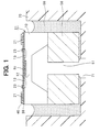
- FIG. 1 is a cross sectional view showing a semiconductor pressure sensor according to a first embodiment of the present invention
- FIG. 2 is a front view showing the pressure sensor of FIG. 1;
- FIG. 3 is a schematic view showing a crystalline axis at a main surface of the pressure sensor of FIG. 1;
- FIG. 4 is an electric circuit view of the pressure sensor of FIG. 1;
- FIG. 5 is a front view showing a reference semiconductor pressure sensor
- FIG. 6A is a line graph showing a relationship between time and square average of output offset of the pressure sensor in the first embodiment
- FIG. 6B is a line graph showing a relationship between time and square average of output offset of the pressure sensor of FIG. 5;
- FIG. 7 is a front view showing a semiconductor pressure sensor according to a second embodiment
- FIG. 8 is a front view showing a semiconductor pressure sensor according to a third embodiment.
- FIG. 9 is a front view showing a semiconductor pressure sensor according to a modification.
- a semiconductor pressure sensor S 1 is produced by using well-known semiconductor production technology for a plane rectangular silicon substrate 10 having a main surface 11 whose plane direction is the (100) plane.
- the pressure sensor S 1 detects minute pressures as small as, for example, 10 kPa.
- a reentrant is formed from a receive surface of the main surface 11 by anisotropy etching with an alkali solution or the like.
- a bottom of the reentrant forms a diaphragm 12 for detecting pressure.
- the shape of diaphragm 12 is an octagon sectioned by the sides that are perpendicular to ⁇ 100> crystalline axis, ⁇ 110> crystalline axis, and ⁇ 111> crystalline axis. However, it may alternatively be formed in the shape of a quadrangle, a circle or the like.
- the diaphragm 12 is sized so as to enable it to detect minute pressures on the order of, for example, 10 kPa.
- a ratio S/d is set larger than 100. Specifically, S is 1.8 ⁇ 10 6 ⁇ m 2 , and d is 13 ⁇ m.
- a plurality of diffusion gauge resistors Rc, Rs are formed in the diaphragm 12 .
- the diffusion gauge resistors Rc, Rs are used for outputting a detection signal that changes based on a change in a resistance value caused by deformation of the diaphragm 12 .
- the diffusion gauge resistors Rs, Rc include two center gauges Rc and two side gauges Rs. Each center gauge Rc is arranged close to a center of the diaphragm 12 . Each side gauge Rs is arranged at a peripheral position of the diaphragm 12 in comparison with the center gauges Rc. Further, the respective diffusion gauge resistors Rs, Rc are arranged along the ⁇ 110> crystalline axis, which is the high sensitivity direction.
- the high sensitivity diffusion gauge resistors Rc, Rs are formed by ion implantation into the main surface 11 and diffusion of the implanted ions.
- the diffusion gauge resistors Rc, Rs are electrically connected to diffusion wiring layers 13 (illustrated by hatching in FIG. 2, FIGS. 5, 7 - 9 are similar, too) that are formed equally by ion implantation into the main surface 11 and by diffusion of the implanted ions.
- the above-mentioned crystalline axis at a main surface of the pressure sensor S 1 is shown in FIG. 3 .
- FIG. 4 Inter-connection of the diffusion gauge resistors Rc, Rs is shown in FIG. 4 .
- a resistance value change of the resistance Rc is opposite to that of resistance Rs.
- each diffusion gauge resistor Rc, Rs is mutually connected in series by diffusion wiring layer 13 (FIG. 1 ). Therefore, a Wheatstone-bridge circuit with a quadrilateral closed circuit is constructed.
- metal wiring segments 21 - 24 are formed on the main surface 11 of a thick portion of the diaphragm 12 .
- the metal wiring segments 21 - 24 connect diffusion gauge resistors Rc, Rs to component outside of the pressure sensor S 1 and are used to apply a voltage to the bridge circuit formed from the diffusion gauge resistors Rc, Rs.
- the metal wiring segments 21 - 24 are used as output lines of the search signal Vout from the bridge circuit.
- the metal wiring segments 21 - 24 specifically include rectangular segments 21 , metal pads 22 , drawer segments 23 and connection segments 24 .
- the rectangular segments 21 form a resistance element and are used to receive an applied substrate electric potential. Respective areas of the rectangular segments 21 are larger than the other metal wiring segments 22 - 24 .
- the metal pads 22 are used to connect non-sensor components to the outside of the pressure sensor S 1 .
- the metal pads 22 are connected with bonding wire.
- the drawer segments 23 electrically connect to the diffusion gauge resistors Rc, Rs via the diffusion wiring layers 13 .
- the connection segments 24 electrically connect the metal pads 22 to rectangular segments 21 .
- the metal wiring segments 21 - 24 are shown by slanted line hatching (FIGS. 5, 7 - 9 are similar, too).
- the metal wiring segments 21 - 24 are formed on an insulation layer 30 such as silicon oxidation layer that is formed on the main surface 11 of the silicon substrate 10 .
- the metal wiring segments 21 - 24 are formed by vapor deposition or the like using aluminum.
- the drawer seguments 23 are electrically connected to the diffusion wiring layers 13 via contact holes formed through the insulation layer 30 .
- the metal wiring segments 21 - 24 are made so as to be spaced from an edge of the diaphragm 12 by a distance of more than 100 ⁇ m on thick portion of the diaphragm 12 .
- a passivating layer 40 for protecting the pressure sensor S 1 covers the metal wiring segments 21 - 24 and insulation layer 30 .
- the passivating layer 40 is made of silicon nitride or the like openings (not shown) are formed at a part of the passivating layer 40 above the metal pads 22 .
- the metal pads 22 electrically connect to outside non-sensor components (not shown) of the pressure sensor S 1 via the openings.
- the semiconductor pressure sensor S 1 can be made by any well-known semiconductor production method. As shown in FIG. 1, the resulting pressure sensor S 1 is bonded into a case 70 . A glass pedestal 50 is joined on the reverse side of the silicon substrate 10 by anode joining or the like. The glass pedestal 50 is fixed on the case 70 by an adhesive 60 made of silicon resin.
- the case 70 is used to install the pressure sensor S 1 in the right position of a measurement target.
- the case 70 is formed from PPS (polyphenylene sulfide), PBT (polybutylene terephthalate) or the like.
- the case 70 has a communication passage 71 for introducing pressure from a measurement target (not shown).
- the pressure of the measurement target is introduced to the pressure sensor S 1 through the reverse side of the diaphragm 12 via the communication passage 71 and through hole 51 .
- the pressure of the measurement target is applied to the diaphragm 12 , and, therefore, the diaphragm 12 is deformed.
- the diffusion gauge resistors Rc, Rs change their resistance value due to deformation of the diaphragm 12 in the direction of the ⁇ 110> crystalline axis.
- the search signal Vout changes based on the resistance value changes in the diffusion gauge resistors Rc, Rs.
- the detection signal Vout is transmitted to an outside circuit (not shown) via metal pads 22 . Then, the detection signal Vout is processed at the outside circuit, and the resulting signal is used as a final output signal.
- the following structure is utilized to repress the creep stress in the metal wiring segments 21 - 24 that acts in the direction of the ⁇ 110> crystalline axis.
- the pressure sensor Si is exposed to high temperatures (e.g., 140° C.) to harden the adhesive 60 and to therefore secure pressure sensor Si to the case 70 .
- high temperatures e.g. 140° C.
- the thermal stress of the metal wiring segments 21 - 24 is moderated over a time period of several hundred hours. Then, stress generated based on the creep stress in metal wiring segments 21 - 24 is supplied to the diaphragm 12 , and the sensor output fluctuates so that the diaphragm 12 is deformed.
- the total area of the metal wiring segments 21 , 22 , 24 arranged on first sides 10 a is larger than the total area of the metal wiring segments 22 , 23 arranged on second sides 10 b.
- the first sides 10 a indicate the sides in parallel with the ⁇ 110> crystalline axis
- the second sides 10 b indicate the sides in parallel with the ⁇ 100> crystalline axis.
- the metal wiring segments 21 , 22 , 24 arranged on the first sides 10 a indicate metal wiring that is closer the first sides 10 a than the second sides 10 b.
- the metal wiring segments 22 , 23 arranged on the second sides 10 b indicate metal wiring that are closer the second sides 10 b than the first sides 10 a. This is obviousness from an arrangement form of the metal wiring segments 21 - 24 shown in FIG. 2 .
- the creep stress in the metal wiring segments 21 - 24 which acts on the diaphragm 12 , mainly acts in the direction of the ⁇ 100> crystalline axis. Therefore, the creep stress that acts the direction of the ⁇ 110> crystalline axis relatively decreases.
- the thick portion that is hard to transform is formed in the direction of the ⁇ 110> crystalline axis while the thin diaphragm 12 that is easy to transform is formed in the direction of the ⁇ 100> crystalline axis, when viewed from metal wiring segments 21 , 22 , 24 that is arranged on the first sides 10 a in parallel with the ⁇ 110> crystalline axis.
- the deformation of the silicon substrate 10 based on the creep stress in the metal wiring segments 21 , 22 , 24 arranged on the first sides 10 a is primarily generated in the direction of the ⁇ 100> crystalline axis.
- the transform of the silicon substrate 10 based on the creep stress in the metal wiring segments 22 , 23 arranged on the second sides 10 b is primarily generated in the direction of the ⁇ 110> crystalline axis.
- the total area of the metal wiring segments 21 , 22 , 24 arranged on a first sides 10 a is larger than the total area of the metal wiring segments 22 , 23 arranged on the second sides 10 b. Therefore, the creep stress in the metal wiring segments 21 - 24 that acts on the diaphragm 12 mainly acts in the direction of the ⁇ 100> crystalline axis, so that the creep stress that acts the direction of the ⁇ 100> crystalline axis relatively decreases.
- a change of the sensor output based on the creep stress in the metal wiring segments 21 - 24 can be repressed when a sensor that can detect minute pressure is utilized as the semiconductor pressure sensor S 1 .
- the rectangular segments 21 having large area were arranged on the second sides 10 b opposite that shown in FIG. 2, i.e., the total area of the metal wiring segments 21 , 22 , 24 arranged on the second sides 10 b were larger than the total area of the metal wiring segments 22 , 23 arranged on the first sides 10 a.
- FIGS. 6A, 6 B indicate the results.
- a square average of offset change that was amplified 1300 times as the sensor output by an amplifier was used as change of sensor offset as against time (unit: hour).
- the diffusion gauge resistors Rc, Rs of the pressure sensor using the 110 type substrate has center gauges Rc and side gauges Rs arranged along the ⁇ 110> crystalline axis.
- the total area of the metal wiring segments 21 , 22 , 24 arranged on first sides 10 a is larger than the total area of the metal wiring segments 22 , 23 arranged on second sides 10 b.
- many of the areas of the metal wiring segments 21 - 24 can be arranged at a far side from the diffusion gauge resistors Rc, Rs in comparison with the comparative example.
- a semiconductor pressure sensor S 2 shown in FIG. 7 represents a modification of the pressure sensor S 1 of the first embodiment. As shown in FIG. 7, this embodiment does not have the rectangular segments 21 shown in FIG. 2 . Namely, the metal wiring includes only metal pads 22 , drawer segments 23 and connection segments 24 .
- each of the drawer segments 23 arranged on the first sides 10 a is also wider than a part of each of the drawer segments 23 arranged on the second sides 10 b. Accordingly, it is possible to obtain the same advantage as the first embodiment.
- a semiconductor pressure sensor S 3 shown in FIG. 8 represents a modification of the pressure sensor S 1 of the second embodiment. Specifically, metal pads 22 are only arranged on the first sides 10 a.
- the total area of the metal pads 22 arranged on first sides 10 a is larger than the total area of the metal pads 22 arranged on second sides 10 b, because the metal pads 22 are formed as the metal wiring segments. Especially, as shown in FIG. 8, it is more preferable that all of the metal pads 22 are arranged on the first sides 10 a.
- the metal pads 22 represent a relatively large portion of the metal wiring segments. Accordingly, in this embodiment, the creep stress in the metal pads 22 that acts the diaphragm 12 mainly acts the direction of the ⁇ 100> crystalline axis, which is virtually unrelated output sensitivity.
- the total area of the metal wiring segments arranged on first sides 10 a is larger than the total area of the metal wiring segments arranged on second sides 10 b. Thus, it is possible to efficiently obtain the same advantage as the first embodiment.
- a semiconductor pressure sensor S 4 shown in FIG. 9 represents yet another modification of the pressure sensor S 1 of the second embodiment. Specifically, drawer segments 23 are only placed on first sides 10 a from the diffusion gauge resistors Rc, Rs.
- the total area of the metal wiring segments arranged on the first sides 10 a is larger than the total area of the metal wiring segments arranged on the second sides 10 b.
Landscapes
- Physics & Mathematics (AREA)
- General Physics & Mathematics (AREA)
- Pressure Sensors (AREA)
- Measuring Fluid Pressure (AREA)
Abstract
Description
Claims (6)
Applications Claiming Priority (2)
| Application Number | Priority Date | Filing Date | Title |
|---|---|---|---|
| JP2001-140556 | 2001-05-10 | ||
| JP2001140556A JP2002340713A (en) | 2001-05-10 | 2001-05-10 | Semiconductor pressure sensor |
Publications (2)
| Publication Number | Publication Date |
|---|---|
| US20020167058A1 US20020167058A1 (en) | 2002-11-14 |
| US6649988B2 true US6649988B2 (en) | 2003-11-18 |
Family
ID=18987145
Family Applications (1)
| Application Number | Title | Priority Date | Filing Date |
|---|---|---|---|
| US10/122,377 Expired - Fee Related US6649988B2 (en) | 2001-05-10 | 2002-04-16 | Semiconductor pressure sensor decreasing creep stress in <110> crystalline axis direction |
Country Status (2)
| Country | Link |
|---|---|
| US (1) | US6649988B2 (en) |
| JP (1) | JP2002340713A (en) |
Cited By (5)
| Publication number | Priority date | Publication date | Assignee | Title |
|---|---|---|---|---|
| US20040177699A1 (en) * | 2003-03-13 | 2004-09-16 | Denso Corporation | Semiconductor pressure sensor |
| US20050062121A1 (en) * | 2003-09-24 | 2005-03-24 | Inao Toyoda | Sensor device having thin membrane and method of manufacturing the same |
| US20150311353A1 (en) * | 2013-12-11 | 2015-10-29 | Melexis Technologies Nv | Semiconductor pressure sensor |
| WO2017133017A1 (en) * | 2016-02-06 | 2017-08-10 | 深圳纽迪瑞科技开发有限公司 | Pressure sensor, electronic device, and method for manufacturing pressure sensor |
| WO2017133016A1 (en) * | 2016-02-06 | 2017-08-10 | 深圳纽迪瑞科技开发有限公司 | Pressure sensor, electronic device, and method for manufacturing pressure sensor |
Families Citing this family (7)
| Publication number | Priority date | Publication date | Assignee | Title |
|---|---|---|---|---|
| JP3915586B2 (en) * | 2002-04-24 | 2007-05-16 | 株式会社デンソー | Method for manufacturing mechanical quantity detection device |
| US20040016981A1 (en) * | 2002-07-26 | 2004-01-29 | Matsushita Electric Works, Ltd. | Semiconductor acceleration sensor using doped semiconductor layer as wiring |
| JP3915715B2 (en) * | 2003-03-07 | 2007-05-16 | 株式会社デンソー | Semiconductor pressure sensor |
| DE102008011942A1 (en) * | 2008-02-29 | 2009-09-03 | Robert Bosch Gmbh | Switching arrangement for converting deformations of membrane of high pressure sensor in motor vehicle into electrical signal, has sensor resistor for detecting signal, and contact surface electrically contacting resistor over feed line |
| JP5673181B2 (en) * | 2011-02-15 | 2015-02-18 | トヨタ自動車株式会社 | Semiconductor device |
| US8466523B2 (en) * | 2011-10-07 | 2013-06-18 | Continental Automotive Systems, Inc. | Differential pressure sensor device |
| US10352792B2 (en) * | 2017-02-15 | 2019-07-16 | Texas Instruments Incorporated | Device and method for on-chip mechanical stress sensing |
Citations (14)
| Publication number | Priority date | Publication date | Assignee | Title |
|---|---|---|---|---|
| US4618397A (en) * | 1982-12-24 | 1986-10-21 | Hitachi, Ltd. | Method of manufacturing semiconductor device having a pressure sensor |
| US4975390A (en) * | 1986-12-18 | 1990-12-04 | Nippondenso Co. Ltd. | Method of fabricating a semiconductor pressure sensor |
| US5081437A (en) * | 1989-02-15 | 1992-01-14 | Schlumberger Industries | Semiconductor pressure sensor |
| US5186054A (en) * | 1989-11-29 | 1993-02-16 | Kabushiki Kaisha Toshiba | Capacitive pressure sensor |
| JPH0755619A (en) | 1993-08-10 | 1995-03-03 | Yamatake Honeywell Co Ltd | Semiconductor pressure sensor |
| US5525549A (en) * | 1992-04-22 | 1996-06-11 | Nippondenso Co., Ltd. | Method for producing an acceleration sensor |
| US5537882A (en) | 1993-10-05 | 1996-07-23 | Ugai; Seiichi | Semiconductor sensor for detecting physical amount without thermal hypsteresis where output wiring is disposed in a stress insensitive direction |
| US5622901A (en) * | 1990-02-08 | 1997-04-22 | Nippondenso Co., Ltd. | Method of forming a semiconductor strain sensor |
| US5643803A (en) * | 1992-09-18 | 1997-07-01 | Nippondenso Co., Ltd. | Production method of a semiconductor dynamic sensor |
| US5654244A (en) * | 1994-04-27 | 1997-08-05 | Nippondenso Co., Ltd. | Process for producing semiconductor strain-sensitive sensor |
| US5770883A (en) * | 1995-09-19 | 1998-06-23 | Nippondenso Co., Ltd. | Semiconductor sensor with a built-in amplification circuit |
| US5920106A (en) * | 1996-12-10 | 1999-07-06 | Denso Corporation | Semiconductor device and method for producing the same |
| US5932921A (en) * | 1996-10-25 | 1999-08-03 | Denso Corporation | Sensor chip having a diode portions and a thin-wall portion |
| US6020618A (en) * | 1994-03-30 | 2000-02-01 | Denso Corporation | Semiconductor device in which thin silicon portions are formed by electrochemical stop etching method |
-
2001
- 2001-05-10 JP JP2001140556A patent/JP2002340713A/en not_active Withdrawn
-
2002
- 2002-04-16 US US10/122,377 patent/US6649988B2/en not_active Expired - Fee Related
Patent Citations (14)
| Publication number | Priority date | Publication date | Assignee | Title |
|---|---|---|---|---|
| US4618397A (en) * | 1982-12-24 | 1986-10-21 | Hitachi, Ltd. | Method of manufacturing semiconductor device having a pressure sensor |
| US4975390A (en) * | 1986-12-18 | 1990-12-04 | Nippondenso Co. Ltd. | Method of fabricating a semiconductor pressure sensor |
| US5081437A (en) * | 1989-02-15 | 1992-01-14 | Schlumberger Industries | Semiconductor pressure sensor |
| US5186054A (en) * | 1989-11-29 | 1993-02-16 | Kabushiki Kaisha Toshiba | Capacitive pressure sensor |
| US5622901A (en) * | 1990-02-08 | 1997-04-22 | Nippondenso Co., Ltd. | Method of forming a semiconductor strain sensor |
| US5525549A (en) * | 1992-04-22 | 1996-06-11 | Nippondenso Co., Ltd. | Method for producing an acceleration sensor |
| US5643803A (en) * | 1992-09-18 | 1997-07-01 | Nippondenso Co., Ltd. | Production method of a semiconductor dynamic sensor |
| JPH0755619A (en) | 1993-08-10 | 1995-03-03 | Yamatake Honeywell Co Ltd | Semiconductor pressure sensor |
| US5537882A (en) | 1993-10-05 | 1996-07-23 | Ugai; Seiichi | Semiconductor sensor for detecting physical amount without thermal hypsteresis where output wiring is disposed in a stress insensitive direction |
| US6020618A (en) * | 1994-03-30 | 2000-02-01 | Denso Corporation | Semiconductor device in which thin silicon portions are formed by electrochemical stop etching method |
| US5654244A (en) * | 1994-04-27 | 1997-08-05 | Nippondenso Co., Ltd. | Process for producing semiconductor strain-sensitive sensor |
| US5770883A (en) * | 1995-09-19 | 1998-06-23 | Nippondenso Co., Ltd. | Semiconductor sensor with a built-in amplification circuit |
| US5932921A (en) * | 1996-10-25 | 1999-08-03 | Denso Corporation | Sensor chip having a diode portions and a thin-wall portion |
| US5920106A (en) * | 1996-12-10 | 1999-07-06 | Denso Corporation | Semiconductor device and method for producing the same |
Cited By (12)
| Publication number | Priority date | Publication date | Assignee | Title |
|---|---|---|---|---|
| US20040177699A1 (en) * | 2003-03-13 | 2004-09-16 | Denso Corporation | Semiconductor pressure sensor |
| US6865951B2 (en) | 2003-03-13 | 2005-03-15 | Denso Corporation | Semiconductor pressure sensor |
| US20050062121A1 (en) * | 2003-09-24 | 2005-03-24 | Inao Toyoda | Sensor device having thin membrane and method of manufacturing the same |
| US7211873B2 (en) * | 2003-09-24 | 2007-05-01 | Denso Corporation | Sensor device having thin membrane and method of manufacturing the same |
| US20150311353A1 (en) * | 2013-12-11 | 2015-10-29 | Melexis Technologies Nv | Semiconductor pressure sensor |
| US10317297B2 (en) * | 2013-12-11 | 2019-06-11 | Melexis Technologies Nv | Semiconductor pressure sensor |
| WO2017133017A1 (en) * | 2016-02-06 | 2017-08-10 | 深圳纽迪瑞科技开发有限公司 | Pressure sensor, electronic device, and method for manufacturing pressure sensor |
| WO2017133016A1 (en) * | 2016-02-06 | 2017-08-10 | 深圳纽迪瑞科技开发有限公司 | Pressure sensor, electronic device, and method for manufacturing pressure sensor |
| CN108604149A (en) * | 2016-02-06 | 2018-09-28 | 深圳纽迪瑞科技开发有限公司 | The production method of pressure sensor, electronic equipment and the pressure sensor |
| US10352799B2 (en) | 2016-02-06 | 2019-07-16 | Shenzhen New Degree Technology Co., Ltd. | Pressure sensor, electronic device, and method for manufacturing pressure sensor |
| US10816416B2 (en) | 2016-02-06 | 2020-10-27 | Shenzhen New Degree Technology Co., Ltd. | Pressure sensor, electronic device, and method for manufacturing pressure sensor |
| CN108604149B (en) * | 2016-02-06 | 2021-06-18 | 深圳纽迪瑞科技开发有限公司 | Pressure sensor, electronic device and method for making the same |
Also Published As
| Publication number | Publication date |
|---|---|
| JP2002340713A (en) | 2002-11-27 |
| US20020167058A1 (en) | 2002-11-14 |
Similar Documents
| Publication | Publication Date | Title |
|---|---|---|
| US6973836B2 (en) | Semiconductor pressure sensor having diaphragm | |
| US8061212B2 (en) | Method of flip chip mounting pressure sensor dies to substrates and pressure sensors formed thereby | |
| US7559247B2 (en) | Pressure sensor with reduced size strain gauge mounting structure and manufacturing method of the same | |
| US7036383B2 (en) | Pressure sensor having sensor chip and signal processing circuit mounted on a common stem | |
| JP5696045B2 (en) | Semiconductor pressure sensor | |
| US6945118B2 (en) | Ceramic on metal pressure transducer | |
| US8186226B2 (en) | Pressure sensor with on-board compensation | |
| US6649988B2 (en) | Semiconductor pressure sensor decreasing creep stress in <110> crystalline axis direction | |
| US10060815B2 (en) | Pressure sensor | |
| US6550339B1 (en) | Pressure sensor for detecting differential pressure between two spaces | |
| JP6154488B2 (en) | Pressure measuring device | |
| KR101213895B1 (en) | Semiconductor strain sensor for vehicle engine intake air pressure measurement | |
| JP2014048072A (en) | Pressure sensor module | |
| KR100210726B1 (en) | Pressure sensor for detecting combustion chamber pressure of internal combustion engine | |
| JPH11153503A (en) | Pressure sensor device | |
| JPS5952727A (en) | Semiconductor pressure sensor | |
| US6543292B1 (en) | Piezoresistive air pressure sensor | |
| JP2009265012A (en) | Semiconductor sensor | |
| JP2512220B2 (en) | Multi-function sensor | |
| JP3120388B2 (en) | Semiconductor pressure transducer | |
| JP2001174352A (en) | Pressure/temperature sensor and pressure/temperature composite detecting element | |
| JPH11258085A (en) | Composite sensor | |
| JPS61245036A (en) | Semiconductor pressure detector | |
| JP3508962B2 (en) | Semiconductor sensor with built-in amplifier circuit | |
| JP2000074767A (en) | Semiconductor pressure sensor |
Legal Events
| Date | Code | Title | Description |
|---|---|---|---|
| AS | Assignment |
Owner name: NIPPON SOKEN, INC., JAPAN Free format text: ASSIGNMENT OF ASSIGNORS INTEREST;ASSIGNORS:TOYODA, INAO;YOSHIDA, TAKAHIKO;ODA, KIYONARI;REEL/FRAME:012804/0020;SIGNING DATES FROM 20020307 TO 20020327 Owner name: DENSO CORPORATION, JAPAN Free format text: ASSIGNMENT OF ASSIGNORS INTEREST;ASSIGNORS:TOYODA, INAO;YOSHIDA, TAKAHIKO;ODA, KIYONARI;REEL/FRAME:012804/0020;SIGNING DATES FROM 20020307 TO 20020327 |
|
| FEPP | Fee payment procedure |
Free format text: PAYOR NUMBER ASSIGNED (ORIGINAL EVENT CODE: ASPN); ENTITY STATUS OF PATENT OWNER: LARGE ENTITY |
|
| FPAY | Fee payment |
Year of fee payment: 4 |
|
| FPAY | Fee payment |
Year of fee payment: 8 |
|
| FEPP | Fee payment procedure |
Free format text: PAYER NUMBER DE-ASSIGNED (ORIGINAL EVENT CODE: RMPN); ENTITY STATUS OF PATENT OWNER: LARGE ENTITY Free format text: PAYOR NUMBER ASSIGNED (ORIGINAL EVENT CODE: ASPN); ENTITY STATUS OF PATENT OWNER: LARGE ENTITY |
|
| REMI | Maintenance fee reminder mailed | ||
| LAPS | Lapse for failure to pay maintenance fees | ||
| STCH | Information on status: patent discontinuation |
Free format text: PATENT EXPIRED DUE TO NONPAYMENT OF MAINTENANCE FEES UNDER 37 CFR 1.362 |
|
| STCH | Information on status: patent discontinuation |
Free format text: PATENT EXPIRED DUE TO NONPAYMENT OF MAINTENANCE FEES UNDER 37 CFR 1.362 |
|
| FP | Lapsed due to failure to pay maintenance fee |
Effective date: 20151118 |