US6649486B1 - Method to form shallow trench isolations - Google Patents
Method to form shallow trench isolations Download PDFInfo
- Publication number
- US6649486B1 US6649486B1 US09/679,510 US67951000A US6649486B1 US 6649486 B1 US6649486 B1 US 6649486B1 US 67951000 A US67951000 A US 67951000A US 6649486 B1 US6649486 B1 US 6649486B1
- Authority
- US
- United States
- Prior art keywords
- layer
- silicon nitride
- protective layer
- angstroms
- semiconductor substrate
- Prior art date
- Legal status (The legal status is an assumption and is not a legal conclusion. Google has not performed a legal analysis and makes no representation as to the accuracy of the status listed.)
- Expired - Lifetime, expires
Links
Images


Classifications
-
- H—ELECTRICITY
- H01—ELECTRIC ELEMENTS
- H01L—SEMICONDUCTOR DEVICES NOT COVERED BY CLASS H10
- H01L21/00—Processes or apparatus adapted for the manufacture or treatment of semiconductor or solid state devices or of parts thereof
- H01L21/70—Manufacture or treatment of devices consisting of a plurality of solid state components formed in or on a common substrate or of parts thereof; Manufacture of integrated circuit devices or of parts thereof
- H01L21/71—Manufacture of specific parts of devices defined in group H01L21/70
- H01L21/76—Making of isolation regions between components
- H01L21/762—Dielectric regions, e.g. EPIC dielectric isolation, LOCOS; Trench refilling techniques, SOI technology, use of channel stoppers
- H01L21/76224—Dielectric regions, e.g. EPIC dielectric isolation, LOCOS; Trench refilling techniques, SOI technology, use of channel stoppers using trench refilling with dielectric materials
- H01L21/76229—Concurrent filling of a plurality of trenches having a different trench shape or dimension, e.g. rectangular and V-shaped trenches, wide and narrow trenches, shallow and deep trenches
Definitions
- the invention relates to a method of fabricating semiconductor devices, and more particularly, to the fabrication of shallow trench isolation structures in the manufacture of an integrated circuit device.
- STI shallow trench isolation
- LOCOS local oxidation of silicon
- FIG. 1 a cross-section of a partially completed prior art integrated circuit is shown.
- trenches 22 and 24 are formed in a semiconductor substrate 10 .
- a pad oxide layer 14 is formed overlying the semiconductor substrate 10 .
- a silicon nitride layer 18 is deposited overlying the pad oxide layer 14 .
- the silicon nitride layer 18 and the pad oxide layer 14 are then patterned to expose the semiconductor substrate 10 where the trenches 22 and 24 are planned.
- the trench etch angle 31 is less than about 70 degrees. Note that this angle 31 is sufficient to form the wide trench 22 but is insufficient to form a flat bottom on the narrow trench 24 .
- the silicon nitride layer 18 has a low etching rate in this trench etch process. Therefore, the thickness of the silicon nitride layer 18 is reduced 30 by only a small amount during the etch process. Variation in the thickness of the silicon nitride layer 18 can cause variation in the thickness of the final STI isolation layer because the silicon nitride layer 18 is the polishing stop for the chemical mechanical polish (CMP) process.
- CMP chemical mechanical polish
- the trench etch angle 32 is increased to between about 75 degrees and 83 degrees. Note that this etch angle 32 is sufficient to form a flat-bottomed narrow trench 24 .
- increasing the trench etching angle brings a disadvantage.
- the etch rate of the silicon nitride layer 18 is also increased. For example, as the trench etch angle increase from 77 degrees to 81 degrees, the silicon nitride layer 18 loss increases from about 300 Angstroms to about 700 Angstroms.
- the second prior art example therefore exhibits a much greater loss 33 of silicon nitride layer 18 due to the trench etching process.
- This loss of hard mask material 18 causes inconsistency and non-uniformity in the thickness of the final STI isolation layer.
- a thicker silicon nitride layer 18 must be deposited to insure that the large angle trench etching process does not punch through.
- increasing the silicon nitride layer 18 thickness also increases the tensile stress and the probability of stress-related device leakage.
- U.S. Pat. No. 6,027,982 to Peidous et al teaches a method to form STI with improved isolation fill and surface planarity. After the trench etch, the silicon nitride masking layer is laterally undercut at the trench edges by etching to thereby expose the substrate surface near the trench edges. A liner oxide layer is then grown in the trenches and the exposed substrate surface. The thin oxide layer overlying the silicon nitride masking layer enables the selective lateral undercutting process.
- U.S. Pat. No. 6,040,231 to Wu discloses an STI process whereby a pad oxide layer is laterally undercut by etching.
- Salicide is then formed in the exposed substrate.
- the salicide is removed to create an a slope periphery on the trenches.
- U.S. Pat. No. 6,057,210 to Yang et al teaches a method to form STI using an indirect CMP process. After trench formation and filling, the trench filling oxide is etched down by a wet etch. A silicon nitride layer is deposited overlying the filling oxide and is then polished down to expose raised portions of the filling oxide. The exposed filling oxide is removed. The silicon nitride layer is removed to complete the STI.
- a principal object of the present invention is to provide an effective and very manufacturable method of fabricating shallow trench isolations in the manufacture of integrated circuits.
- a further object of the present invention is to provide a method to fabricate narrow trenches for shallow trench isolations by facilitating the use of a large trench etching angle process.
- a further object of the present invention is to provide a method to use a large trench etching angle while avoiding silicon nitride masking layer loss.
- Another further object of the present invention is to reduce variation in STI thickness due to silicon nitride layer loss during the trench etch process.
- a yet further object of the present invention is to prevent silicon nitride masking layer loss through the use of an overlying protective layer.
- Another yet further object of the present invention is to reduce silicon nitride masking layer loss due to high density plasma sputtering.
- a pad oxide layer is formed overlying a semiconductor substrate.
- a silicon nitride layer is deposited overlying the pad oxide layer.
- a protective layer is deposited overlying the silicon nitride layer.
- the protective layer, the silicon nitride layer, and the pad oxide layer are patterned to expose the semiconductor substrate where shallow trench isolations are planned.
- the semiconductor substrate is etched to form trenches for the planned shallow trench isolations. A large trench etching angle is used.
- the presence of the protective layer prevents etching of the silicon nitride layer during the etching.
- a trench filling layer is deposited overlying the protective layer and filling the trenches. The trench filling layer and the protective layer are polished down to complete the shallow trench isolations in the manufacture of the integrated circuit device.
- FIGS. 1 and 2 schematically illustrate in cross-section partially completed prior art integrated circuit devices.
- FIGS. 3 through 7 schematically illustrate in cross-sectional representation a preferred embodiment of the present invention.
- the method of the present invention is applied to the formation of shallow trench isolation structures in a semiconductor substrate.
- the present invention can be applied and extended without deviating from the scope of the present invention.
- a semiconductor substrate 50 is provided.
- the semiconductor substrate 50 comprises monocrystalline silicon fabricated by methods well known in the art.
- a pad oxide layer 54 is formed overlying the semiconductor substrate 50 .
- the pad oxide layer 54 is used to improve the adhesion of the subsequently deposited silicon nitride layer.
- the pad oxide layer 54 is preferably formed by thermal oxidation of the semiconductor substrate 50 .
- the pad oxide layer 54 is preferably formed to a thickness of between about 50 Angstroms and 250 Angstroms.
- a silicon nitride layer 58 is next deposited overlying the pad oxide layer 54 .
- the silicon nitride layer 58 serves as a hard mask during trench etching.
- the silicon nitride layer 58 may be deposited by, for example, a low-pressure chemical vapor deposition (LPCVD) process. It is important to the present invention that the silicon nitride layer 58 be deposited thin enough to keep tensile stress low. By keeping the tensile stress low, the probability of stress-related device leakage is reduced.
- the ability to use a thinner silicon nitride layer 58 in conjunction with a large trench etching angle is a distinct advantage to the present invention.
- the silicon nitride layer 58 is deposited to a thickness of less than about 1300 Angstroms and preferably between about 600 Angstroms and 1,300 Angstroms.
- the prior art scheme cannot use such a thin silicon nitride layer with a large trench etching angle process.
- a protective layer 62 is deposited overlying the silicon nitride layer 58 .
- the protective layer protects the silicon nitride layer 58 so that the silicon nitride layer 58 is not lost during the trench etch.
- the protective layer 62 comprises a material of low selectivity to silicon nitride etching and high selectivity to silicon etching.
- the protective layer 62 preferably comprises silicon dioxide deposited by low-pressure TEOS (LP-TEOS) chemical vapor deposition (CVD).
- the protective layer 62 may comprise SiO x N y (stoichiometric silicon oxynitride), AP (atmospheric pressure) TEOS CVD, or SA (sub-atmospheric) TEOS CVD.
- the protective layer 62 be deposited to a great enough thickness to protect the silicon nitride layer Se during the entire trench etch process. Since the protective layer 62 is etched down during the trench etching process, the protective layer 62 must be deposited to a thickness of between about 200 Angstroms and 800 Angstroms. A thinner protective layer 62 will not protect the silicon nitride layer 58 from loss and, therefore, will allow variation in STI thickness after polish down.
- the protective layer 62 , the silicon nitride layer 58 , and the pad oxide layer 54 are patterned to expose the semiconductor substrate 50 where shallow trench isolations are planned.
- the patterning is accomplished by, for example, depositing a photoresist layer overlying the protective layer 62 .
- the photoresist layer not shown, would then be exposed to actinic light through a mask.
- the protective layer 62 is exposed where trenches are planned.
- the protective layer 62 , the silicon nitride layer 58 , and the pad oxide layer 54 are then etched through using, for example, a plasma dry etch process.
- the silicon nitride layer 58 thereby forms a hard mask for the trench etching step.
- the remaining photoresist is stripped away.
- wide trenches 66 and narrow trenches 68 are formed.
- the semiconductor substrate 50 is etched where it is exposed. Trenches 66 and 68 are formed for the planned shallow trench isolations.
- a large trench etching angle 72 is used.
- the large trench etching angle 72 produces steep trench sidewalls 70 and a flat bottom in the narrow trenches 68 .
- the etching angle 72 is the angle at which the plasma ions strike the semiconductor substrate 50 surface.
- the large trench etching angle 72 is controlled to between about 75 degrees and 88 degrees.
- the use of a large trench etching angle 72 can cause a rapid loss of the silicon nitride layer 58 .
- the novel protective layer 62 of the present invention protects the silicon nitride layer 58 for the trench etch. Therefore, no appreciable silicon nitride layer 58 loss occurs.
- the protective layer 62 is reduced 74 in thickness during the etch. However, since the protective layer 62 is made sufficiently thick, it does not punch through to reveal the underlying silicon nitride layer 58 .
- a filling layer 78 is deposited overlying the protective layer 62 and filling the trenches.
- the filling layer 78 serves as an electrical insulator, or dielectric barrier, for the STI structures.
- the filling layer 78 preferably comprises a high density plasma (HDP) deposited silicon dioxide layer. HDP oxide exhibits excellent trench filling qualities.
- HDP oxide exhibits excellent trench filling qualities.
- LP-TEOS, AP-TEOS, or oxygen-rich SiO x N y may be used as the filling layer 78 material.
- the presence of the novel protective layer 62 protects the silicon nitride layer 58 during the depositing of the HDP oxide filling layer 78 .
- Such a high density plasma process can cause sputtering of the silicon nitride layer 58 that would reduce the nitride layer thickness.
- the protective layer 62 prevents the loss of the silicon nitride layer 58 during the HDP process.
- the trench filling layer 78 and the protective layer 62 are polished down to complete the shallow trench isolations in the manufacture of the integrated circuit device.
- the polishing preferably comprises a chemical mechanical polish (CMP).
- CMP chemical mechanical polish
- the silicon nitride layer 58 is the polishing stop. Since the protective layer 62 of the present invention protects silicon nitride layer 58 throughout the trench etching and filling sequence, the thickness of the silicon nitride layer 58 is maintained. Therefore, a uniform STI height is achieved across the device wafer.
- the advantages of the process of the present invention can now be enumerated.
- Second, the method allows the use of a large trench etching angle to thereby form very narrow trenches.
- the present invention provides a very manufacturable process for fabricating shallow trench isolations while protecting the silicon nitride masking layer in the manufacture of an integrated circuit device.
Landscapes
- Engineering & Computer Science (AREA)
- Physics & Mathematics (AREA)
- Condensed Matter Physics & Semiconductors (AREA)
- General Physics & Mathematics (AREA)
- Manufacturing & Machinery (AREA)
- Computer Hardware Design (AREA)
- Microelectronics & Electronic Packaging (AREA)
- Power Engineering (AREA)
- Element Separation (AREA)
Abstract
A new method of fabricating shallow trench isolations has been achieved. A pad oxide layer is formed overlying a semiconductor substrate. A silicon nitride layer is deposited overlying the pad oxide layer. A protective layer is deposited overlying the silicon nitride layer. The protective layer, the silicon nitride layer, and the pad oxide layer are patterned to expose the semiconductor substrate where shallow trench isolations are planned. The semiconductor substrate is etched to form trenches for the planned shallow trench isolations. A large trench etching angle is used. The presence of the protective layer prevents loss of the silicon nitride layer during the etching. A trench filling layer is deposited overlying the protective layer and filling the trenches. The trench filling layer and the protective layer are polished down to complete the shallow trench isolations in the manufacture of the integrated circuit device.
Description
1 Field of the Invention
The invention relates to a method of fabricating semiconductor devices, and more particularly, to the fabrication of shallow trench isolation structures in the manufacture of an integrated circuit device.
2 Description of the Prior Art
The use of shallow trench isolation (STI) for the formation of integrated circuit isolations has grown in the art due to the reduced surface area and improved topology of STI when compared to traditional local oxidation of silicon (LOCOS) schemes. However, as the space between active regions shrinks with advancing technology, it is becoming more challenging to form STI.
Referring to FIG. 1, a cross-section of a partially completed prior art integrated circuit is shown. In this first prior art example, trenches 22 and 24 are formed in a semiconductor substrate 10. Prior to formation of the trenches, a pad oxide layer 14 is formed overlying the semiconductor substrate 10. A silicon nitride layer 18 is deposited overlying the pad oxide layer 14. The silicon nitride layer 18 and the pad oxide layer 14 are then patterned to expose the semiconductor substrate 10 where the trenches 22 and 24 are planned.
The trenches 22 and 24 are then etched using an anisotropic dry plasma etching process. In the first prior art example, the trench etch angle 31 is less than about 70 degrees. Note that this angle 31 is sufficient to form the wide trench 22 but is insufficient to form a flat bottom on the narrow trench 24. The silicon nitride layer 18 has a low etching rate in this trench etch process. Therefore, the thickness of the silicon nitride layer 18 is reduced 30 by only a small amount during the etch process. Variation in the thickness of the silicon nitride layer 18 can cause variation in the thickness of the final STI isolation layer because the silicon nitride layer 18 is the polishing stop for the chemical mechanical polish (CMP) process.
Referring now to FIG. 2, a second example of a prior art STI is illustrated. In this example, the trench etch angle 32 is increased to between about 75 degrees and 83 degrees. Note that this etch angle 32 is sufficient to form a flat-bottomed narrow trench 24. However, increasing the trench etching angle brings a disadvantage. By increasing the angle at which the ionic plasma strikes the wafer surface, the etch rate of the silicon nitride layer 18 is also increased. For example, as the trench etch angle increase from 77 degrees to 81 degrees, the silicon nitride layer 18 loss increases from about 300 Angstroms to about 700 Angstroms. The second prior art example therefore exhibits a much greater loss 33 of silicon nitride layer 18 due to the trench etching process. This loss of hard mask material 18 causes inconsistency and non-uniformity in the thickness of the final STI isolation layer. At a minimum, a thicker silicon nitride layer 18 must be deposited to insure that the large angle trench etching process does not punch through. However, increasing the silicon nitride layer 18 thickness also increases the tensile stress and the probability of stress-related device leakage.
Several prior art approaches disclose methods to form shallow trench isolation in the semiconductor substrate. U.S. Pat. No. 6,027,982 to Peidous et al teaches a method to form STI with improved isolation fill and surface planarity. After the trench etch, the silicon nitride masking layer is laterally undercut at the trench edges by etching to thereby expose the substrate surface near the trench edges. A liner oxide layer is then grown in the trenches and the exposed substrate surface. The thin oxide layer overlying the silicon nitride masking layer enables the selective lateral undercutting process. U.S. Pat. No. 6,040,231 to Wu discloses an STI process whereby a pad oxide layer is laterally undercut by etching. Salicide is then formed in the exposed substrate. The salicide is removed to create an a slope periphery on the trenches. U.S. Pat. No. 6,057,210 to Yang et al teaches a method to form STI using an indirect CMP process. After trench formation and filling, the trench filling oxide is etched down by a wet etch. A silicon nitride layer is deposited overlying the filling oxide and is then polished down to expose raised portions of the filling oxide. The exposed filling oxide is removed. The silicon nitride layer is removed to complete the STI.
A principal object of the present invention is to provide an effective and very manufacturable method of fabricating shallow trench isolations in the manufacture of integrated circuits.
A further object of the present invention is to provide a method to fabricate narrow trenches for shallow trench isolations by facilitating the use of a large trench etching angle process.
A further object of the present invention is to provide a method to use a large trench etching angle while avoiding silicon nitride masking layer loss.
Another further object of the present invention is to reduce variation in STI thickness due to silicon nitride layer loss during the trench etch process.
A yet further object of the present invention is to prevent silicon nitride masking layer loss through the use of an overlying protective layer.
Another yet further object of the present invention is to reduce silicon nitride masking layer loss due to high density plasma sputtering.
In accordance with the objects of this invention, a new method of fabricating shallow trench isolations has been achieved. A pad oxide layer is formed overlying a semiconductor substrate. A silicon nitride layer is deposited overlying the pad oxide layer. A protective layer is deposited overlying the silicon nitride layer. The protective layer, the silicon nitride layer, and the pad oxide layer are patterned to expose the semiconductor substrate where shallow trench isolations are planned. The semiconductor substrate is etched to form trenches for the planned shallow trench isolations. A large trench etching angle is used. The presence of the protective layer prevents etching of the silicon nitride layer during the etching. A trench filling layer is deposited overlying the protective layer and filling the trenches. The trench filling layer and the protective layer are polished down to complete the shallow trench isolations in the manufacture of the integrated circuit device.
In the accompanying drawings forming a material part of this description, there is shown:
FIGS. 1 and 2 schematically illustrate in cross-section partially completed prior art integrated circuit devices.
FIGS. 3 through 7 schematically illustrate in cross-sectional representation a preferred embodiment of the present invention.
The method of the present invention is applied to the formation of shallow trench isolation structures in a semiconductor substrate. In should be clear to those experienced in the art that the present invention can be applied and extended without deviating from the scope of the present invention.
Referring now more particularly to FIG. 3, there is illustrated a cross-section of a partially completed integrated circuit device of the preferred embodiment. Several important features of the present invention are illustrated. A semiconductor substrate 50 is provided. Preferably, the semiconductor substrate 50 comprises monocrystalline silicon fabricated by methods well known in the art. A pad oxide layer 54 is formed overlying the semiconductor substrate 50. The pad oxide layer 54 is used to improve the adhesion of the subsequently deposited silicon nitride layer. The pad oxide layer 54 is preferably formed by thermal oxidation of the semiconductor substrate 50. The pad oxide layer 54 is preferably formed to a thickness of between about 50 Angstroms and 250 Angstroms.
A silicon nitride layer 58 is next deposited overlying the pad oxide layer 54. The silicon nitride layer 58 serves as a hard mask during trench etching. The silicon nitride layer 58 may be deposited by, for example, a low-pressure chemical vapor deposition (LPCVD) process. It is important to the present invention that the silicon nitride layer 58 be deposited thin enough to keep tensile stress low. By keeping the tensile stress low, the probability of stress-related device leakage is reduced. The ability to use a thinner silicon nitride layer 58 in conjunction with a large trench etching angle is a distinct advantage to the present invention. Therefore, the silicon nitride layer 58 is deposited to a thickness of less than about 1300 Angstroms and preferably between about 600 Angstroms and 1,300 Angstroms. The prior art scheme cannot use such a thin silicon nitride layer with a large trench etching angle process.
A protective layer 62 is deposited overlying the silicon nitride layer 58. The protective layer protects the silicon nitride layer 58 so that the silicon nitride layer 58 is not lost during the trench etch. The protective layer 62 comprises a material of low selectivity to silicon nitride etching and high selectivity to silicon etching. The protective layer 62 preferably comprises silicon dioxide deposited by low-pressure TEOS (LP-TEOS) chemical vapor deposition (CVD). Alternatively, the protective layer 62 may comprise SiOxNy (stoichiometric silicon oxynitride), AP (atmospheric pressure) TEOS CVD, or SA (sub-atmospheric) TEOS CVD. Finally, a combination these above films may be used. It is very important that the protective layer 62 be deposited to a great enough thickness to protect the silicon nitride layer Se during the entire trench etch process. Since the protective layer 62 is etched down during the trench etching process, the protective layer 62 must be deposited to a thickness of between about 200 Angstroms and 800 Angstroms. A thinner protective layer 62 will not protect the silicon nitride layer 58 from loss and, therefore, will allow variation in STI thickness after polish down.
Referring now to FIG. 4, the protective layer 62, the silicon nitride layer 58, and the pad oxide layer 54 are patterned to expose the semiconductor substrate 50 where shallow trench isolations are planned. The patterning is accomplished by, for example, depositing a photoresist layer overlying the protective layer 62. The photoresist layer, not shown, would then be exposed to actinic light through a mask. After development, the protective layer 62 is exposed where trenches are planned. The protective layer 62, the silicon nitride layer 58, and the pad oxide layer 54 are then etched through using, for example, a plasma dry etch process. The silicon nitride layer 58 thereby forms a hard mask for the trench etching step. Finally, the remaining photoresist is stripped away. In the example of the preferred embodiment, wide trenches 66 and narrow trenches 68 are formed.
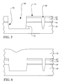
Referring now to FIG. 5, an important feature of the present invention is illustrated. The semiconductor substrate 50 is etched where it is exposed. Trenches 66 and 68 are formed for the planned shallow trench isolations. A large trench etching angle 72 is used. The large trench etching angle 72 produces steep trench sidewalls 70 and a flat bottom in the narrow trenches 68. The etching angle 72 is the angle at which the plasma ions strike the semiconductor substrate 50 surface. Preferably, the large trench etching angle 72 is controlled to between about 75 degrees and 88 degrees.
As noted in the prior art analysis, the use of a large trench etching angle 72 can cause a rapid loss of the silicon nitride layer 58. However, the novel protective layer 62 of the present invention protects the silicon nitride layer 58 for the trench etch. Therefore, no appreciable silicon nitride layer 58 loss occurs. The protective layer 62 is reduced 74 in thickness during the etch. However, since the protective layer 62 is made sufficiently thick, it does not punch through to reveal the underlying silicon nitride layer 58.
Referring now to FIG. 6, a filling layer 78 is deposited overlying the protective layer 62 and filling the trenches. The filling layer 78 serves as an electrical insulator, or dielectric barrier, for the STI structures. The filling layer 78 preferably comprises a high density plasma (HDP) deposited silicon dioxide layer. HDP oxide exhibits excellent trench filling qualities. Alternatively, LP-TEOS, AP-TEOS, or oxygen-rich SiOxNy may be used as the filling layer 78 material.
Note that the presence of the novel protective layer 62 protects the silicon nitride layer 58 during the depositing of the HDP oxide filling layer 78. Such a high density plasma process can cause sputtering of the silicon nitride layer 58 that would reduce the nitride layer thickness. The protective layer 62 prevents the loss of the silicon nitride layer 58 during the HDP process.
Referring now to FIG. 7, the trench filling layer 78 and the protective layer 62 are polished down to complete the shallow trench isolations in the manufacture of the integrated circuit device. The polishing preferably comprises a chemical mechanical polish (CMP). The silicon nitride layer 58 is the polishing stop. Since the protective layer 62 of the present invention protects silicon nitride layer 58 throughout the trench etching and filling sequence, the thickness of the silicon nitride layer 58 is maintained. Therefore, a uniform STI height is achieved across the device wafer.
The advantages of the process of the present invention can now be enumerated. First, an effective process for forming shallow trench isolation has been achieved. Second, the method allows the use of a large trench etching angle to thereby form very narrow trenches. Third, a protective layer overlies the silicon nitride masking layer so that the large trench etching angle can be used. Fourth, good uniformity of STI thickness is achieved by protecting the silicon nitride layer.
As shown in the preferred embodiment, the present invention provides a very manufacturable process for fabricating shallow trench isolations while protecting the silicon nitride masking layer in the manufacture of an integrated circuit device.
While the invention has been particularly shown and described with reference to the preferred embodiments thereof, it will be understood by those skilled in the art that various changes in form and details may be made without departing from the spirit and scope of the invention.
Claims (15)
1. A method of forming trenches for shallow trench isolation structures in an integrated circuit device comprising:
providing a semiconductor substrate;
forming a pad oxide layer overlying said semiconductor substrate;
depositing a silicon nitride layer overlying said pad oxide layer;
depositing a protective layer overlying said silicon nitride layer wherein said protective layer comprises SiOxNy (stoichiometric silicon oxynitride);
patterning said protective layer, said silicon nitride layer, and said pad oxide layer to expose said semiconductor substrate where trenches for shallow trench isolations are planned; and
etching said semiconductor substrate to complete said trenches in the manufacture of the integrated circuit device wherein the presence of said protective layer prevents loss of said silicon nitride layer during said etching.
2. The method according to claim 1 wherein said pad oxide layer is formed to a thickness of between about 50 Angstroms and 250 Angstroms.
3. The method according to claim 1 wherein said silicon nitride layer is deposited to a thickness of between about 600 Angstroms and 1,300 Angstroms.
4. The method according to claim 1 wherein said protective layer is deposited to a thickness of between about 200 Angstroms and 800 Angstroms.
5. The method according to claim 1 further comprising:
depositing a trench filling layer overlying said protective layer and filling said trenches after said step of etching said semiconductor substrate; and
polishing down said trench filling layer and said protective layer.
6. The method according to claim 5 wherein said trench filling layer comprises one of the group of: high density plasma (HDP) oxide, LP-TEOS, AP-TEOS, and oxygen-rich SiOxNy.
7. A method of forming trenches for shallow trench isolation structures in an integrated circuit device comprising:
providing a semiconductor substrate;
forming a pad oxide layer overlying said semiconductor substrate;
depositing a silicon nitride layer overlying said pad oxide layer;
depositing a protective layer overlying said silicon nitride layer wherein said protective layer comprises SiOxNy (stoichiometric silicon oxynitride);
patterning said protective layer, said silicon nitride layer, and said pad oxide layer to expose said semiconductor substrate where trenches for shallow trench isolations are planned; and
etching said semiconductor substrate to complete said trenches in the manufacture of the integrated circuit device wherein the presence of said protective layer prevents loss of said silicon nitride layer during said etching.
8. The method according to claim 7 wherein said pad oxide layer is formed to a thickness of between about 50 Angstroms and 250 Angstroms.
9. The method according to claim 7 wherein said silicon nitride layer is deposited to a thickness of between about 600 Angstroms and 1,300 Angstroms.
10. The method according to claim 7 wherein said protective layer is deposited to a thickness of between about 200 Angstroms and 800 Angstroms.
11. The method according to claim 7 further comprising:
depositing a trench filling layer overlying said protective layer and filling said trenches after said step of etching said semiconductor substrate; and
polishing down said trench filling layer and said protective layer.
12. The method according to claim 11 wherein said trench filling layer comprises one of the group of: high density plasma (HDP) oxide, LP-TEOS, AP-TEOS, and oxygen-rich SiOxNy.
13. A method of forming shallow trench isolations in an integrated circuit device comprising:
providing a semiconductor substrate;
forming a pad oxide layer overlying said semiconductor substrate;
depositing a silicon nitride layer overlying said pad oxide layer wherein said silicon nitride layer is deposited to a thickness of between about 600 Angstroms and 1,300 Angstroms;
depositing a protective layer overlying said silicon nitride layer wherein said protective layer comprises SiOxNy (stoichiometric silicon oxynitride);
patterning said protective layer, said silicon nitride layer, and said pad oxide layer to expose said semiconductor substrate where shallow trench isolations are planned;
etching said semiconductor substrate to form trenches for said planned shallow trench isolations wherein the presence of said protective layer prevents etching of said silicon nitride layer during said etching;
depositing a trench filling layer overlying said protective layer and filling said trenches; and
polishing down said trench filling layer and said protective layer to complete said shallow trench isolations in the manufacture of the integrated circuit device.
14. The method according to claim 13 wherein said pad oxide layer is formed to a thickness of between about 50 Angstroms and 250 Angstroms.
15. The method according to claim 13 wherein said protective layer is deposited to a thickness of between about 200 Angstroms and 800 Angstroms.
Priority Applications (2)
| Application Number | Priority Date | Filing Date | Title |
|---|---|---|---|
| US09/679,510 US6649486B1 (en) | 2000-10-06 | 2000-10-06 | Method to form shallow trench isolations |
| SG200105922A SG106060A1 (en) | 2000-10-06 | 2001-09-27 | A method to form shallow trench isolations |
Applications Claiming Priority (1)
| Application Number | Priority Date | Filing Date | Title |
|---|---|---|---|
| US09/679,510 US6649486B1 (en) | 2000-10-06 | 2000-10-06 | Method to form shallow trench isolations |
Publications (1)
| Publication Number | Publication Date |
|---|---|
| US6649486B1 true US6649486B1 (en) | 2003-11-18 |
Family
ID=29420823
Family Applications (1)
| Application Number | Title | Priority Date | Filing Date |
|---|---|---|---|
| US09/679,510 Expired - Lifetime US6649486B1 (en) | 2000-10-06 | 2000-10-06 | Method to form shallow trench isolations |
Country Status (2)
| Country | Link |
|---|---|
| US (1) | US6649486B1 (en) |
| SG (1) | SG106060A1 (en) |
Cited By (6)
| Publication number | Priority date | Publication date | Assignee | Title |
|---|---|---|---|---|
| US20050139949A1 (en) * | 2003-12-31 | 2005-06-30 | Dongbuanam Semiconductor Inc. | Shallow trench isolation structure and formation method thereof |
| US20060151838A1 (en) * | 2005-01-12 | 2006-07-13 | International Business Machines Corporation | Enhanced pfet using shear stress |
| US20140326699A1 (en) * | 2013-05-02 | 2014-11-06 | HGST Netherlands B.V. | Pmr overwrite enhancement by main pole rie method |
| CN104217985A (en) * | 2013-05-31 | 2014-12-17 | 中芯国际集成电路制造(上海)有限公司 | Semiconductor device and fabrication method of shallow trench |
| CN104282614A (en) * | 2013-07-01 | 2015-01-14 | 中芯国际集成电路制造(上海)有限公司 | Method for forming shallow-trench isolating structure |
| US9263067B1 (en) * | 2013-05-29 | 2016-02-16 | Western Digital (Fremont), Llc | Process for making PMR writer with constant side wall angle |
Citations (11)
| Publication number | Priority date | Publication date | Assignee | Title |
|---|---|---|---|---|
| US6027982A (en) | 1999-02-05 | 2000-02-22 | Chartered Semiconductor Manufacturing Ltd. | Method to form shallow trench isolation structures with improved isolation fill and surface planarity |
| US6037237A (en) * | 1997-07-25 | 2000-03-14 | Samsung Electronics Co., Ltd. | Trench isolation methods utilizing composite oxide films |
| US6040231A (en) | 1998-01-23 | 2000-03-21 | United Microelectronics Corp. | Method of fabricating a shallow trench isolation structure which includes using a salicide process to form an aslope periphery at the top corner of the substrate |
| US6057210A (en) | 1998-04-21 | 2000-05-02 | Vanguard International Semiconductor Corporation | Method of making a shallow trench isolation for ULSI formation via in-direct CMP process |
| US6080637A (en) * | 1998-12-07 | 2000-06-27 | Taiwan Semiconductor Manufacturing Company | Shallow trench isolation technology to eliminate a kink effect |
| US6110797A (en) * | 1999-12-06 | 2000-08-29 | National Semiconductor Corporation | Process for fabricating trench isolation structure for integrated circuits |
| US6140242A (en) * | 1997-12-01 | 2000-10-31 | Samsung Electronics Co., Ltd. | Method of forming an isolation trench in a semiconductor device including annealing at an increased temperature |
| US6180490B1 (en) * | 1999-05-25 | 2001-01-30 | Chartered Semiconductor Manufacturing Ltd. | Method of filling shallow trenches |
| US6261914B1 (en) * | 1999-07-27 | 2001-07-17 | International Business Machines Corporation | Process for improving local uniformity of chemical mechanical polishing using a self-aligned polish rate enhancement layer |
| US6284623B1 (en) * | 1999-10-25 | 2001-09-04 | Peng-Fei Zhang | Method of fabricating semiconductor devices using shallow trench isolation with reduced narrow channel effect |
| US6287974B1 (en) * | 1999-06-30 | 2001-09-11 | Lam Research Corporation | Method of achieving top rounding and uniform etch depths while etching shallow trench isolation features |
-
2000
- 2000-10-06 US US09/679,510 patent/US6649486B1/en not_active Expired - Lifetime
-
2001
- 2001-09-27 SG SG200105922A patent/SG106060A1/en unknown
Patent Citations (11)
| Publication number | Priority date | Publication date | Assignee | Title |
|---|---|---|---|---|
| US6037237A (en) * | 1997-07-25 | 2000-03-14 | Samsung Electronics Co., Ltd. | Trench isolation methods utilizing composite oxide films |
| US6140242A (en) * | 1997-12-01 | 2000-10-31 | Samsung Electronics Co., Ltd. | Method of forming an isolation trench in a semiconductor device including annealing at an increased temperature |
| US6040231A (en) | 1998-01-23 | 2000-03-21 | United Microelectronics Corp. | Method of fabricating a shallow trench isolation structure which includes using a salicide process to form an aslope periphery at the top corner of the substrate |
| US6057210A (en) | 1998-04-21 | 2000-05-02 | Vanguard International Semiconductor Corporation | Method of making a shallow trench isolation for ULSI formation via in-direct CMP process |
| US6080637A (en) * | 1998-12-07 | 2000-06-27 | Taiwan Semiconductor Manufacturing Company | Shallow trench isolation technology to eliminate a kink effect |
| US6027982A (en) | 1999-02-05 | 2000-02-22 | Chartered Semiconductor Manufacturing Ltd. | Method to form shallow trench isolation structures with improved isolation fill and surface planarity |
| US6180490B1 (en) * | 1999-05-25 | 2001-01-30 | Chartered Semiconductor Manufacturing Ltd. | Method of filling shallow trenches |
| US6287974B1 (en) * | 1999-06-30 | 2001-09-11 | Lam Research Corporation | Method of achieving top rounding and uniform etch depths while etching shallow trench isolation features |
| US6261914B1 (en) * | 1999-07-27 | 2001-07-17 | International Business Machines Corporation | Process for improving local uniformity of chemical mechanical polishing using a self-aligned polish rate enhancement layer |
| US6284623B1 (en) * | 1999-10-25 | 2001-09-04 | Peng-Fei Zhang | Method of fabricating semiconductor devices using shallow trench isolation with reduced narrow channel effect |
| US6110797A (en) * | 1999-12-06 | 2000-08-29 | National Semiconductor Corporation | Process for fabricating trench isolation structure for integrated circuits |
Non-Patent Citations (1)
| Title |
|---|
| Chang et al, ULSI Technology, McGraw-Hill, 1996, p. 215-217. * |
Cited By (11)
| Publication number | Priority date | Publication date | Assignee | Title |
|---|---|---|---|---|
| US20050139949A1 (en) * | 2003-12-31 | 2005-06-30 | Dongbuanam Semiconductor Inc. | Shallow trench isolation structure and formation method thereof |
| US7339251B2 (en) | 2003-12-31 | 2008-03-04 | Dongbu Electronics Co., Ltd. | Shallow trench isolation structure and formation method thereof |
| US20060151838A1 (en) * | 2005-01-12 | 2006-07-13 | International Business Machines Corporation | Enhanced pfet using shear stress |
| WO2006076535A1 (en) | 2005-01-12 | 2006-07-20 | International Business Machines Corporation | Enhanced pfet using shear stress |
| US7274084B2 (en) | 2005-01-12 | 2007-09-25 | International Business Machines Corporation | Enhanced PFET using shear stress |
| US20140326699A1 (en) * | 2013-05-02 | 2014-11-06 | HGST Netherlands B.V. | Pmr overwrite enhancement by main pole rie method |
| US9449635B2 (en) * | 2013-05-02 | 2016-09-20 | HGST Netherlands B.V. | Method for forming a magnetic head for perpendicular magnetic recording |
| US9263067B1 (en) * | 2013-05-29 | 2016-02-16 | Western Digital (Fremont), Llc | Process for making PMR writer with constant side wall angle |
| CN104217985A (en) * | 2013-05-31 | 2014-12-17 | 中芯国际集成电路制造(上海)有限公司 | Semiconductor device and fabrication method of shallow trench |
| CN104282614A (en) * | 2013-07-01 | 2015-01-14 | 中芯国际集成电路制造(上海)有限公司 | Method for forming shallow-trench isolating structure |
| CN104282614B (en) * | 2013-07-01 | 2017-09-01 | 中芯国际集成电路制造(上海)有限公司 | A kind of method for forming fleet plough groove isolation structure |
Also Published As
| Publication number | Publication date |
|---|---|
| SG106060A1 (en) | 2004-09-30 |
Similar Documents
| Publication | Publication Date | Title |
|---|---|---|
| US6228727B1 (en) | Method to form shallow trench isolations with rounded corners and reduced trench oxide recess | |
| US6008106A (en) | Micro-trench oxidation by using rough oxide mask for field isolation | |
| US6727159B2 (en) | Method of forming a shallow trench isolation in a semiconductor substrate | |
| US6033970A (en) | Method for forming device-isolating layer in semiconductor device | |
| KR100224700B1 (en) | Isolation method of semiconductor device | |
| US6251734B1 (en) | Method for fabricating trench isolation and trench substrate contact | |
| US6306723B1 (en) | Method to form shallow trench isolations without a chemical mechanical polish | |
| US6784077B1 (en) | Shallow trench isolation process | |
| US6207534B1 (en) | Method to form narrow and wide shallow trench isolations with different trench depths to eliminate isolation oxide dishing | |
| US6518148B1 (en) | Method for protecting STI structures with low etching rate liners | |
| US6339004B1 (en) | Method of forming shallow trench isolation for preventing torn oxide | |
| US6599813B2 (en) | Method of forming shallow trench isolation for thin silicon-on-insulator substrates | |
| US20030203515A1 (en) | Method of forming a shallow trench isolation structure | |
| US6475875B1 (en) | Shallow trench isolation elevation uniformity via insertion of a polysilicon etch layer | |
| US6277710B1 (en) | Method of forming shallow trench isolation | |
| KR100234416B1 (en) | Method of forming a device isolation film of semiconductor device | |
| US6649486B1 (en) | Method to form shallow trench isolations | |
| US6355539B1 (en) | Method for forming shallow trench isolation | |
| US6232203B1 (en) | Process for making improved shallow trench isolation by employing nitride spacers in the formation of the trenches | |
| US6225225B1 (en) | Method to form shallow trench isolation structures for borderless contacts in an integrated circuit | |
| US6180492B1 (en) | Method of forming a liner for shallow trench isolation | |
| US6391739B1 (en) | Process of eliminating a shallow trench isolation divot | |
| US6667222B1 (en) | Method to combine zero-etch and STI-etch processes into one process | |
| US6232181B1 (en) | Method of forming a flash memory | |
| US6444539B1 (en) | Method for producing a shallow trench isolation filled with thermal oxide |
Legal Events
| Date | Code | Title | Description |
|---|---|---|---|
| AS | Assignment |
Owner name: CHARTERED SEMICONDUCTOR MANUFACTURING, LTD., SINGA Free format text: ASSIGNMENT OF ASSIGNORS INTEREST;ASSIGNORS:BALAKUMAR, SUBRMANIAN;LEE, KONG HEAN;ZHOU, ZHENG;AND OTHERS;REEL/FRAME:011197/0965 Effective date: 20000901 |
|
| STCF | Information on status: patent grant |
Free format text: PATENTED CASE |
|
| CC | Certificate of correction | ||
| FPAY | Fee payment |
Year of fee payment: 4 |
|
| FPAY | Fee payment |
Year of fee payment: 8 |
|
| FPAY | Fee payment |
Year of fee payment: 12 |
|
| SULP | Surcharge for late payment |
Year of fee payment: 11 |