US6646637B1 - Liquid crystal display device - Google Patents
Liquid crystal display device Download PDFInfo
- Publication number
- US6646637B1 US6646637B1 US09/709,434 US70943400A US6646637B1 US 6646637 B1 US6646637 B1 US 6646637B1 US 70943400 A US70943400 A US 70943400A US 6646637 B1 US6646637 B1 US 6646637B1
- Authority
- US
- United States
- Prior art keywords
- liquid crystal
- switches
- display device
- crystal display
- circuit
- Prior art date
- Legal status (The legal status is an assumption and is not a legal conclusion. Google has not performed a legal analysis and makes no representation as to the accuracy of the status listed.)
- Expired - Lifetime, expires
Links
Images


Classifications
-
- G—PHYSICS
- G09—EDUCATION; CRYPTOGRAPHY; DISPLAY; ADVERTISING; SEALS
- G09G—ARRANGEMENTS OR CIRCUITS FOR CONTROL OF INDICATING DEVICES USING STATIC MEANS TO PRESENT VARIABLE INFORMATION
- G09G3/00—Control arrangements or circuits, of interest only in connection with visual indicators other than cathode-ray tubes
- G09G3/20—Control arrangements or circuits, of interest only in connection with visual indicators other than cathode-ray tubes for presentation of an assembly of a number of characters, e.g. a page, by composing the assembly by combination of individual elements arranged in a matrix no fixed position being assigned to or needed to be assigned to the individual characters or partial characters
- G09G3/2007—Display of intermediate tones
- G09G3/2011—Display of intermediate tones by amplitude modulation
-
- G—PHYSICS
- G09—EDUCATION; CRYPTOGRAPHY; DISPLAY; ADVERTISING; SEALS
- G09G—ARRANGEMENTS OR CIRCUITS FOR CONTROL OF INDICATING DEVICES USING STATIC MEANS TO PRESENT VARIABLE INFORMATION
- G09G3/00—Control arrangements or circuits, of interest only in connection with visual indicators other than cathode-ray tubes
- G09G3/20—Control arrangements or circuits, of interest only in connection with visual indicators other than cathode-ray tubes for presentation of an assembly of a number of characters, e.g. a page, by composing the assembly by combination of individual elements arranged in a matrix no fixed position being assigned to or needed to be assigned to the individual characters or partial characters
- G09G3/34—Control arrangements or circuits, of interest only in connection with visual indicators other than cathode-ray tubes for presentation of an assembly of a number of characters, e.g. a page, by composing the assembly by combination of individual elements arranged in a matrix no fixed position being assigned to or needed to be assigned to the individual characters or partial characters by control of light from an independent source
- G09G3/36—Control arrangements or circuits, of interest only in connection with visual indicators other than cathode-ray tubes for presentation of an assembly of a number of characters, e.g. a page, by composing the assembly by combination of individual elements arranged in a matrix no fixed position being assigned to or needed to be assigned to the individual characters or partial characters by control of light from an independent source using liquid crystals
- G09G3/3611—Control of matrices with row and column drivers
- G09G3/3685—Details of drivers for data electrodes
- G09G3/3688—Details of drivers for data electrodes suitable for active matrices only
-
- G—PHYSICS
- G09—EDUCATION; CRYPTOGRAPHY; DISPLAY; ADVERTISING; SEALS
- G09G—ARRANGEMENTS OR CIRCUITS FOR CONTROL OF INDICATING DEVICES USING STATIC MEANS TO PRESENT VARIABLE INFORMATION
- G09G2310/00—Command of the display device
- G09G2310/02—Addressing, scanning or driving the display screen or processing steps related thereto
- G09G2310/0243—Details of the generation of driving signals
- G09G2310/0248—Precharge or discharge of column electrodes before or after applying exact column voltages
-
- G—PHYSICS
- G09—EDUCATION; CRYPTOGRAPHY; DISPLAY; ADVERTISING; SEALS
- G09G—ARRANGEMENTS OR CIRCUITS FOR CONTROL OF INDICATING DEVICES USING STATIC MEANS TO PRESENT VARIABLE INFORMATION
- G09G2310/00—Command of the display device
- G09G2310/02—Addressing, scanning or driving the display screen or processing steps related thereto
- G09G2310/0243—Details of the generation of driving signals
- G09G2310/0251—Precharge or discharge of pixel before applying new pixel voltage
-
- G—PHYSICS
- G09—EDUCATION; CRYPTOGRAPHY; DISPLAY; ADVERTISING; SEALS
- G09G—ARRANGEMENTS OR CIRCUITS FOR CONTROL OF INDICATING DEVICES USING STATIC MEANS TO PRESENT VARIABLE INFORMATION
- G09G2310/00—Command of the display device
- G09G2310/02—Addressing, scanning or driving the display screen or processing steps related thereto
- G09G2310/0264—Details of driving circuits
- G09G2310/027—Details of drivers for data electrodes, the drivers handling digital grey scale data, e.g. use of D/A converters
Definitions
- the present invention relates to a liquid crystal display device which incorporates a peripheral circuit and which is designed to receive a digital signal input.
- a conventional technique for production of multi-gradation display for a liquid crystal display device is, for example, disclosed in JP-A-5-333817 (1993).
- FIGS. 16A through 16D of the accompanying drawings are views which may be used to illustrate a principle of operation of a D/A conversion circuit which is driven with less reference voltages than the number of gradations to be output, in accordance with the technique disclosed in the above-referenced patent document.
- this D/A conversion circuit five gradation voltages are generated at an output VX from two reference voltages VA and VB.
- a switch 91 is a low resistance switch and a switch 92 is a high resistance switch.
- a switch 92 is a high resistance switch.
- voltages formed by equally dividing the reference voltages VA and VB by four are outputted with respect to the lowest two bits (D 1 , D 0 ) of input signal representing gradations to be displayed.
- the D/A conversion circuit can be driven with less reference voltages than the number of gradations to be outputted. Further, by reducing the number of low resistance switches, which require a large area on a semiconductor chip, the area occupied by a driving circuit is reduced, and, thus, the non-display area in the liquid crystal display device can be reduced.
- the D/A conversion circuit when the D/A conversion circuit is constituted by parallel circuits of high resistance switches and low resistance switches for more than two reference voltages, the output resistance of the D/A conversion circuit varies depending on the input signals representing gradations to be displayed.
- load capacitances exist, including an OFF capacitance and an ON capacitance, formed by the switches constituting the D/A conversion circuit and the capacitance of a drain line, therefore, these capacitances also need to be driven. Further, these capacitances are independent from the input signals representing gradations to be displayed and are substantially invariable.
- FIG. 17 is a graph representing the relationship between short voltage/varying input voltage and conversion time.
- the abscissa represents the D/A conversion time and the ordinate represents the short voltage/varying input voltage as a logarithm.
- the inclination of the attenuation is determined by a product of the load capacitance and the output resistance and varies depending on the output resistance.
- the ratio of the short voltage 0.002 as it is for the maximum resistance Rmax at the D/A conversion lower limit Tc roughly corresponds to the unevenness or variation of the short voltage, in that it is 16 mV. Since the unevenness in the short voltage appears depending on the gradations, if the D/A conversion time is shortened from the D/A conversion lower limit Tc, this may lead to deterioration of the picture quality because of voltage interval variation between adjacent gradations.
- An object of the present invention is to provide a liquid crystal display device in which the output resistance of a D/A conversion circuit is kept at a constant value regardless of the gradations to be displayed.
- a liquid crystal display device comprises a pair of substrates at least one of which is transparent, a liquid crystal layer sandwiched between the substrates, a display region and a peripheral circuit for driving the display region, both of which are mounted on one of the pair of substrates.
- the display region is formed by a plurality of drain lines and a plurality of gate lines arranged in a matrix shape, and a plurality of thin film transistors are each disposed near the respective cross points of the matrix.
- the peripheral circuit is provided with a driving circuit which is signed to receive digital image signal inputs.
- the driving circuit is provided with a plurality of D/A conversion circuits, each being constituted by a plurality of switches, each having substantially the same ON resistance, and a control unit which controls ON and OFF operation of the switches in such a manner that, at the time of a D/A conversion operation, a plurality of switches in a corresponding number are turned ON for respective input signals representing respective gradations.
- the D/A conversion circuit can be constituted by a plurality of switch groups, each being constituted by a plurality of switches connected in parallel.
- One of the terminals of each of the respective switch groups is respectively connected to different wiring lines for supplying respectively different reference voltages, the other terminals of the switch groups are connected in common to constitute a voltage output portion, and the control unit operates to turn ON a predetermined number n of switches among one or two of the switch groups.
- R represents a center value of ON resistances of the switches
- r represents the difference between the maximum value and the minimum value of the ON resistances of the switches
- n represents the number of switches being turned ON at the same time, as referred to above.
- control unit operates to turn ON all of the switches belonging to one switch group in an early stage of the D/A conversion time.
- a distribution circuit can be provided which distributes the output voltages of the D/A conversion circuit to a plurality of drain lines.
- a pre-charge circuit can be provided which applies a voltage to the drain lines for every horizontal one line period.
- the switch can be constituted either by a single thin film transistor or by a parallel connection of a plurality of thin film transistors, the source electrodes and drain electrodes of which are respectively connected in common or by series connection of a thin film transistor and a resistor.
- FIG. 1 is a block diagram of a liquid crystal display device representing a first embodiment according to the present invention
- FIG. 2 is a schematic circuit diagram showing a D/A conversion circuit used in the FIG. 1 embodiment
- FIG. 3 is a diagram showing an exemplary operation performed in a control circuit in the D/A conversion circuit in the FIG. 1 embodiment
- FIGS. 4A through 4D are diagrams which may be used to illustrated the manner of voltage generation in a D/A conversion circuit in a liquid crystal display device according to the present invention.
- FIG. 5 is a diagram illustrating a case in which an error voltage maximizes in the D/A conversion circuit in the liquid crystal display device according to the present invention
- FIGS. 6A and 6B are diagrams showing the resistances in switch groups in a case in which an error voltage maximizes in the D/A conversion circuit in the liquid crystal display device according to the present invention
- FIG. 7 is a diagram showing another exemplary operation performed in a control circuit in the D/A conversion circuit in the FIG. 1 embodiment
- FIG. 8 is an equivalent circuit diagram of a switch constituting a D/A conversion circuit in a liquid crystal display device according to the present invention.
- FIG. 9 is another equivalent circuit diagram of a switch for constituting a D/A conversion circuit in a liquid crystal display device according to the present invention.
- FIG. 10 is still another equivalent circuit diagram of a switch for constituting a D/A conversion circuit in a liquid crystal display device according to the present invention.
- FIG. 11 is a block diagram of a liquid crystal display device representing a second embodiment according to the present invention.
- FIG. 12 is a schematic circuit diagram of a distribution circuit used in the FIG. 11 embodiment.
- FIG. 13 is a diagram showing an exemplary operation performed in a control circuit in the D/A conversion circuit in the FIG. 11 embodiment
- FIG. 14 is a diagram showing another exemplary operation performed in a control circuit in the D/A conversion circuit in the FIG. 11 embodiment
- FIG. 15 is a block diagram of a liquid crystal display device representing a third embodiment according to the present invention.
- FIGS. 16A through 16D are diagrams which may be used to illustrate an operating principle of a D/A conversion circuit in a conventional liquid crystal display device.
- FIG. 17 is a diagram for explaining a manner of change of short voltages with respect to conversion time when output resistances in a D/A conversion circuit differ.
- FIG. 1 is a diagram showing the constitution of a liquid crystal display device representing a first embodiment of the present invention. As illustrated in the drawing, on the surface of an insulating substrate 1 in the liquid crystal display device, a display region 2 , a drain driver 3 and a gate driver 4 are provided.
- the display region 2 is constituted by drain lines DL and gate lines SL, which are arranged in a matrix shape, and pixel TFTs (Thin Film Transistors) 5 and display electrodes PX, which are arranged for every intersection point of the drain lines DL and the gate lines SL.
- pixel TFTs Thin Film Transistors
- FIG. 1 in order to facilitate understanding of the constitution of the liquid crystal display device, only two drain lines DL and two gate lines SL are illustrated.
- VGA type Video Graphic Array
- the number of the gate lines SL is 480
- the number of drain lines DL is 1920.
- the drain driver 3 is constituted by TFTs and is provided with D/A conversion circuits DA 1 through DA 4 .
- D/A conversion circuits DA 1 through DA 4 To one drain line DL, a pair of D/A conversion circuits, for example, DA 1 and DA 2 , are connected, and to the pair of D/A conversion circuits DA 1 and DA 2 , reference voltage distribution lines VA 1 through VA 5 and VB 1 through VB 5 are respectively connected.
- reference voltages in a higher range of the liquid crystal drive voltage are supplied, and to the reference voltage distribution lines VB 1 through VB 5 , reference voltages in a lower range of the liquid crystal drive voltage are supplied.
- the D/A conversion circuits DA 2 and DA 4 are operated, and when generating voltages in the lower range of the liquid crystal drive voltage at the drain line DL, the D/A conversion circuits DA 1 and DA 3 are operated. Thereby, the liquid crystal panel is AC-driven.
- the gate driver 4 is constituted by TFTs and is connected, to all of the gate lines SL.
- the gate driver 4 turns ON a pixel TFT 5 connected to a specific gate line SL and determines a display electrode PX which samples a voltage at the drain line DL.
- FIG. 2 is a circuit diagram showing a circuit arrangement of one of the D/A conversion circuits DA 1 through DA 4 , for example, DA 1 .
- the D/A conversion circuit DA 1 is a circuit with 4 bit inputs and 16 gradation outputs. Of course, the number of bits and gradations of the D/A conversion circuit is not limited to these specific numbers.
- the D/A conversion circuit DA 1 is constituted by switches S 1 through S 19 and a control circuit CTL which controls ON and OFF operation of the switches S 1 through S 19 .
- the switches S 1 through S 4 are connected in parallel by connecting respective input and output terminals in common and constitute a switch group SG 1 .
- the switches S 5 through S 8 constitute a switch group SG 2
- the switches S 9 through S 12 constitute a switch group SG 3
- the switches S 13 through S 16 constitute a switch group SG 4
- the switches S 17 through S 19 constitute a switch group SG 5 .
- Input terminals of the switch groups SG 1 through SG 5 are respectively connected to reference voltage input terminals V 0 through V 4 , and all of the output terminals of the switch groups SG 1 through SG 5 are connected in common and are connected to an output terminal Vout.
- switches S 1 through S 19 are connected to output terminals Y 1 through Y 19 of the control circuit CTL.
- the outputs from the output terminals Y 1 through Y 19 are binary logic signals through which the ON and OFF operation of the switches S 1 through S 19 are controlled.
- control circuit CTL To the control circuit CTL 4, bit data signals and an output enable signal EN (not shown) are inputted.
- the control circuit CTL varies the outputs at the output terminals Y 1 through Y 19 according to image signals inputted to the 4 bit data signal lines and the output enable signal EN, and thereby controls ON/OFF operation of the switches S 1 through S 19 .
- FIG. 3 is a diagram showing an example of the operation of the control circuit CTL.
- the control circuit CTL when the input signal data is 0, the control circuit CTL outputs signals to the output terminals Y 1 through Y 19 to turn ON switches S 1 through S 4 and turn OFF all of the other switches, whereas, when the input signal data is 1, the control circuit CTL outputs signals to the output terminals Y 1 through Y 19 to turn ON the switches S 2 through S 5 and turn OFF all of the other switches.
- the control circuit CTL outputs signals to the output terminals Y 1 through Y 19 to turn ON specific ones of four successive switches Sk+1 through Sk+4 and to turn OFF all of the other remaining switches.
- the control circuit CTL outputs signals to the output terminals Y 1 through Y 19 to turn OFF all of the switches S 1 through S 19 .
- the output terminal Vout is cut off from the reference voltages and the function of the D/A conversion circuit is inhibited.
- FIG. 1 since a pair of D/A conversion circuits are connected to a single drain line DL, by alternately operating the two D/A conversion circuits using the output enable signal EN, the voltage supplied to the drain line is alternated between the higher and lower ranges.
- FIGS. 4A through 4D are diagrams illustrating the relationship between input signal data, output voltage and output resistance in the D/A conversion circuits DA 1 through DA 4 , wherein the ON resistance value of one switch is assumed as R.
- Vk and Vout are connected by four switches connected in parallel as shown in FIG. 4 A.
- the voltage Vout assumes the value Vk, and the output resistance of Vout is R/4.
- the output resistance of Vout in these instances also gives R/4.
- each of the D/A conversion circuits DA 1 through DA 4 can generate 16 gradation voltages from the five reference voltages, in other words, they can generate more gradation voltages than the number of reference voltages. Further, in these instances, the output resistance of the D/A conversion circuit is reduced to R/4 which is smaller than the ON resistance of a single switch. Still further, the output resistance of the respective D/A conversion circuits always is R/4 regardless of the input signals representing gradations to be displayed.
- gradation inversion implies a phenomena in which an inverted portion is generated in a relationship between dark and bright with regard to the gradation to be displayed.
- FIG. 5 An instance when such an error voltage is maximized is represented by the following case illustrated in FIG. 5, in which a half number of switches n/2 in two switch groups each constituted by n switches are turned ON, and the ON resistance of one of the two switch groups assumes a minimum value and the other of the two switch groups assumes a maximum value.
- FIGS. 6A and 6B show two cases in which the resistances of two switch groups give the above values. Namely, in FIG.
- the resistance of the switch group SGk connected to the reference voltage Vk is (R+r/2)/(n/2) and the resistance of the switch group SGk+1 connected to the reference voltage Vk+1 is (R ⁇ r/2)/(n/2); and, in FIG. 6B, the resistance of the switch group SGk connected to the reference voltage Vk is (R ⁇ r/2)/(2/n) and the resistance of the switch group SGk+1 connected to the reference voltage Vk+1 is (R+r/2)/(n/2).
- the maximum error voltage being generated is given as
- r/2Rx
- the error voltage is kept low and at least below the voltage corresponding to one gradation. Since the voltage band corresponding to one gradation is
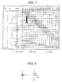
- FIG. 7 is a diagram showing another example of an operation performed by the control circuit CTL.
- S signals are inputted to the control circuit CTL in addition to the data signals and the EN signal.
- the control circuit CTL can utilize a repeating structure which simplifies the circuit arrangement.
- FIG. 8 is a diagram showing an example of a circuit arrangement of one of the switches S 1 through S 19 .
- the switch is constituted by a single TFT.
- the channel width and length of the respective TFTs are equalized.
- P channel TFTs are used for the D/A conversion circuits DA 2 and DA 4 , which cover a higher voltage range in the liquid crystal drive voltage
- n channel TFTs are used for the D/A conversion circuits DA 1 and DA 3 , which cover a lower voltage range in the liquid crystal drive voltage
- the ON resistances of the respective switches can further be reduced.
- FIG. 9 is a diagram showing another circuit arrangement of one of the switches S 1 through S 19 .
- a plurality of TFTs are connected in parallel and the respective electrodes of the gates, sources and drains are connected in common.
- the channel width and length of the respective TFTs are similarly equalized. Further, when a plurality of TFTs are used, an unevenness of the ON resistances of the respective TFTs is averaged and a stable resistance value can be obtained, in contrast to what is obtained with the use of a single TFT.
- FIG. 10 is a diagram showing still another circuit arrangement of one of the switches S 1 through S 19 .
- the switch is constituted by connecting in series a single TFT and a resistance element formed by a wiring material.
- the channel width and length of the respective TFTs are similarly equalized.
- a stable resistance value can be obtained, in contrast to what is obtained with the use of a TFT alone.
- a plurality of TFTs connected in parallel as shown in FIG. 9, can be used for the single TFT.
- FIG. 11 is a block diagram showing a circuit arrangement of a liquid crystal display device representing a second embodiment of the present invention.
- the circuit arrangement of the present liquid crystal display device is basically the same as FIG. 1 embodiment except for the circuit arrangement of the drain driver.
- the drain driver 3 a in the present liquid crystal display device is constituted by D/A conversion circuits DA 1 through DA 4 and distribution circuits MP 1 and MP 2 .
- the drain driver 3 a is constituted by adding the distribution circuits MP 1 and MP 2 to the drain driver circuit 3 in the FIG. 1 embodiment.
- the circuit arrangement of the D/A conversion circuits DA 1 through DA 4 is the same as that shown in FIG. 2 for the FIG. 1 embodiment. Further, like the FIG. 1 embodiment, reference voltages in a lower range of the liquid crystal drive voltage are supplied to the D/A conversion circuits DA 1 and DA 3 via the reference voltage distribution lines VB 1 ⁇ VB 5 , and reference voltages in a higher range of the liquid crystal drive voltage are supplied to the D/A conversion circuits DA 2 and DA 4 via the reference voltage distribution lines VA 1 ⁇ VA 5 .
- the voltages generated by the D/A conversion circuits DA 1 ⁇ DA 4 are distributed by the distribution circuits MP 1 and MP 2 to a plurality of drain lines DL.
- the distributed voltage is first held by the capacity CD of the drain lines.
- the voltage held by the capacity CD is sampled via a pixel TFT 5 , which is turned ON by the gate driver 4 by a corresponding display electrode PX.
- the distribution circuits MP 1 and MP 2 output a voltage which is received at input terminal i 1 or i 2 to one of the output terminals o 1 ⁇ o 4 according to a control signal.
- the voltage received at the input terminal i 1 is outputted to one of the output terminals o 1 ⁇ o 4
- the voltage received at the input terminal i 2 is outputted to one of the output terminals o 1 ⁇ o 4 .
- the D/A conversion circuit when the D/A conversion circuit outputs a voltage to be outputted to a drain line DL connected to the output terminal o 1 , a voltage received at input terminal i 1 or i 2 is outputted to the output terminal o 1 ; when the D/A conversion circuit outputs a voltage to be outputted to a drain line DL connected to the output terminal o 2 , a voltage received at input terminal i 1 or i 2 is outputted to the output terminal o 2 ; when the D/A conversion circuit outputs a voltage to be outputted to a drain line DL connected to the output terminal o 3 , a voltage received at input terminal i 1 or i 2 is outputted to the output terminal o 3 ; and when the D/A conversion circuit outputs a voltage to be outputted to a drain line DL connected to the output terminal o 4 , a voltage received at input terminal i 1 or i 2 is outputted to the output terminal o 4 .
- the D/A conversion circuits are used
- FIG. 12 shows a circuit diagram of one of the distribution circuits MP 1 and MP 2 .
- the present distribution circuit is constituted by a plurality of switches 81 which are connected in such a manner that all of the input terminals i 1 and i 2 are connected to all of the output terminals o 1 ⁇ o 4 .
- a plurality of drain lines DL can be driven by one D/A conversion circuit, therefore, the number of D/A conversion circuits can be reduced.
- FIG. 13 is a diagram showing an example of an operation performed by the control circuit CTL.
- the change-over of the D/A conversion circuits for example, between DA 1 and DA 2 is performed in the distribution circuits MP 1 and MP 2 , therefore, the EN signal control in the control circuit is unnecessary.
- the parasitic capacitances of the TFTs constituting the switches in the D/A conversion circuits and the distribution circuits and the capacitances CD of the drain lines are included.
- the capacitances CD of the drain lines are equal to or larger than the total f the parasitic capacitances of the TFTs constituting the switches in the D/A conversion circuits and the distribution circuits, the capacitances CD of the drain lines become dominant, and, therefore, it becomes necessary to make the ON resistances of the switches 81 constituting the distribution circuits substantially equal to each other.
- FIG. 14 is a diagram showing another example of an operation of the control circuit CTL.
- the change-over of the D/A conversion circuits is performed in the distribution circuits MP 1 and MP 2 , therefore, the EN signal control in the control circuit is unnecessary.
- FIG. 15 is a circuit diagram showing a circuit arrangement of a liquid crystal display device representing a third embodiment of the present invention.
- the present embodiment is constituted by adding a pre-charge circuit to the second embodiment as shown in FIG. 11 .
- Other constituting elements of the present embodiment are the same as those in FIG. 11 embodiment.
- the pre-charge circuit 6 is connected to all of the drain lines and pre-charges the drain lines with a predetermined voltage for every horizontal one line period.
- the drain lines are pre-charged to a predetermined voltage by the pre-charge circuit 6 , and, thereafter, the drain lines are charged by the D/A conversion circuit to a target voltage, therefore, a varying voltage band is kept constant for every gradation. Accordingly, the variation of the short voltage is further reduced in comparison with the second embodiment shown in FIG. 11 .
- a plurality of switches constituting D/A conversion circuits incorporated in a liquid crystal display device are turned ON at the same time, and the number of switches which are turned on at the same time is constant regardless of the input signals representing gradations; therefore, the output resistances of the respective D/A conversion circuits become constant and are smaller than the ON resistance of one of the switches, and, additionally, the unevenness of the short voltage of the D/A conversion circuits is reduced in comparison with the conventional arrangement. Thereby, an improvement in image quality and multi-gradation are easily achieved in comparison with the conventional arrangement. Moreover, the D/A conversion time can be shortened, thereby, a high resolution in a liquid crystal display device can be easily achieved.
Landscapes
- Engineering & Computer Science (AREA)
- Physics & Mathematics (AREA)
- Computer Hardware Design (AREA)
- General Physics & Mathematics (AREA)
- Theoretical Computer Science (AREA)
- Chemical & Material Sciences (AREA)
- Crystallography & Structural Chemistry (AREA)
- Liquid Crystal (AREA)
- Liquid Crystal Display Device Control (AREA)
- Control Of Indicators Other Than Cathode Ray Tubes (AREA)
- Analogue/Digital Conversion (AREA)
Abstract
Description
Claims (26)
Applications Claiming Priority (2)
| Application Number | Priority Date | Filing Date | Title |
|---|---|---|---|
| JP2000054958A JP4031897B2 (en) | 2000-02-29 | 2000-02-29 | Liquid crystal display |
| JP2000-054958 | 2000-02-29 |
Publications (1)
| Publication Number | Publication Date |
|---|---|
| US6646637B1 true US6646637B1 (en) | 2003-11-11 |
Family
ID=18576153
Family Applications (1)
| Application Number | Title | Priority Date | Filing Date |
|---|---|---|---|
| US09/709,434 Expired - Lifetime US6646637B1 (en) | 2000-02-29 | 2000-11-13 | Liquid crystal display device |
Country Status (2)
| Country | Link |
|---|---|
| US (1) | US6646637B1 (en) |
| JP (1) | JP4031897B2 (en) |
Cited By (5)
| Publication number | Priority date | Publication date | Assignee | Title |
|---|---|---|---|---|
| US20030174118A1 (en) * | 2002-01-08 | 2003-09-18 | Tomohiko Sato | Display device |
| US20030193490A1 (en) * | 2002-04-11 | 2003-10-16 | Biing-Der Liu | Display driving circuit |
| US20060017683A1 (en) * | 2002-05-02 | 2006-01-26 | Sony Corporation | Display device, method for driving the same, and portable terminal apparatus using the same |
| US20090121980A1 (en) * | 2006-06-30 | 2009-05-14 | Canon Kabushiki Kaisha | Display apparatus and information processing apparatus using the same |
| CN111710310A (en) * | 2020-06-30 | 2020-09-25 | 厦门天马微电子有限公司 | Multi-path distribution circuit, array substrate, display panel, device and driving method |
Families Citing this family (1)
| Publication number | Priority date | Publication date | Assignee | Title |
|---|---|---|---|---|
| JP3926651B2 (en) * | 2002-01-21 | 2007-06-06 | シャープ株式会社 | Display drive device and display device using the same |
Citations (6)
| Publication number | Priority date | Publication date | Assignee | Title |
|---|---|---|---|---|
| US6191779B1 (en) * | 1997-07-11 | 2001-02-20 | Kabushiki Kaisha Toshiba | Liquid crystal display device, device for controlling drive of liquid crystal display device and D/A converting semiconductor device |
| US6225931B1 (en) * | 1999-08-30 | 2001-05-01 | Industrial Technology Research Institute | D/A converter with a gamma correction circuit |
| US6373459B1 (en) * | 1998-06-03 | 2002-04-16 | Lg Semicon Co., Ltd. | Device and method for driving a TFT-LCD |
| US6392354B1 (en) * | 1998-05-20 | 2002-05-21 | Seiko Epson Corporation | Electro-optical element driving circuit, electro-optical device, and electronic device |
| US6411273B1 (en) * | 1997-04-22 | 2002-06-25 | Matsushita Electric Industrial Co., Ltd. | Drive circuit for active matrix liquid crystal display |
| US6424328B1 (en) * | 1998-03-19 | 2002-07-23 | Sony Corporation | Liquid-crystal display apparatus |
-
2000
- 2000-02-29 JP JP2000054958A patent/JP4031897B2/en not_active Expired - Fee Related
- 2000-11-13 US US09/709,434 patent/US6646637B1/en not_active Expired - Lifetime
Patent Citations (6)
| Publication number | Priority date | Publication date | Assignee | Title |
|---|---|---|---|---|
| US6411273B1 (en) * | 1997-04-22 | 2002-06-25 | Matsushita Electric Industrial Co., Ltd. | Drive circuit for active matrix liquid crystal display |
| US6191779B1 (en) * | 1997-07-11 | 2001-02-20 | Kabushiki Kaisha Toshiba | Liquid crystal display device, device for controlling drive of liquid crystal display device and D/A converting semiconductor device |
| US6424328B1 (en) * | 1998-03-19 | 2002-07-23 | Sony Corporation | Liquid-crystal display apparatus |
| US6392354B1 (en) * | 1998-05-20 | 2002-05-21 | Seiko Epson Corporation | Electro-optical element driving circuit, electro-optical device, and electronic device |
| US6373459B1 (en) * | 1998-06-03 | 2002-04-16 | Lg Semicon Co., Ltd. | Device and method for driving a TFT-LCD |
| US6225931B1 (en) * | 1999-08-30 | 2001-05-01 | Industrial Technology Research Institute | D/A converter with a gamma correction circuit |
Cited By (9)
| Publication number | Priority date | Publication date | Assignee | Title |
|---|---|---|---|---|
| US20030174118A1 (en) * | 2002-01-08 | 2003-09-18 | Tomohiko Sato | Display device |
| US7167154B2 (en) * | 2002-01-08 | 2007-01-23 | Hitachi, Ltd. | Display device |
| US20030193490A1 (en) * | 2002-04-11 | 2003-10-16 | Biing-Der Liu | Display driving circuit |
| US7102630B2 (en) * | 2002-04-11 | 2006-09-05 | Au Optronics Corp. | Display driving circuit |
| US20060017683A1 (en) * | 2002-05-02 | 2006-01-26 | Sony Corporation | Display device, method for driving the same, and portable terminal apparatus using the same |
| US7372446B2 (en) * | 2002-05-02 | 2008-05-13 | Sony Corporation | Display device, method for driving the same, and portable terminal apparatus using the same |
| US20090121980A1 (en) * | 2006-06-30 | 2009-05-14 | Canon Kabushiki Kaisha | Display apparatus and information processing apparatus using the same |
| US8432380B2 (en) * | 2006-06-30 | 2013-04-30 | Canon Kabushiki Kaisha | Display apparatus and information processing apparatus using the same |
| CN111710310A (en) * | 2020-06-30 | 2020-09-25 | 厦门天马微电子有限公司 | Multi-path distribution circuit, array substrate, display panel, device and driving method |
Also Published As
| Publication number | Publication date |
|---|---|
| JP4031897B2 (en) | 2008-01-09 |
| JP2001242837A (en) | 2001-09-07 |
Similar Documents
| Publication | Publication Date | Title |
|---|---|---|
| US9601076B2 (en) | Source driver that generates from image data an interpolated output signal for use by a flat panel display and methods thereof | |
| US6232948B1 (en) | Liquid crystal display driving circuit with low power consumption and precise voltage output | |
| US7006114B2 (en) | Display driving apparatus and display apparatus using same | |
| US7034797B2 (en) | Drive circuit, electro-optical device and driving method thereof | |
| KR100701834B1 (en) | Display device and drive circuit for display device | |
| US8537092B2 (en) | Shared buffer display panel drive methods and systems | |
| EP0723695B1 (en) | Power-saving circuit and method for driving liquid crystal display | |
| US7994956B2 (en) | Digital-to-analog converter circuit, data driver, and display device using the digital-to-analog converter circuit | |
| US8111184B2 (en) | Digital-to-analog converting circuit, data driver and display device | |
| US7474306B2 (en) | Display panel including a plurality of drivers having common wires each for providing reference voltage | |
| US5818406A (en) | Driver circuit for liquid crystal display device | |
| US20060050037A1 (en) | Impedance conversion circuit, drive circuit, and control method of impedance conversion circuit | |
| US7961167B2 (en) | Display device having first and second vertical drive circuits | |
| US7245283B2 (en) | LCD source driving circuit having reduced structure including multiplexing-latch circuits | |
| US7477271B2 (en) | Data driver, display device, and method for controlling data driver | |
| US6646637B1 (en) | Liquid crystal display device | |
| CN100511385C (en) | Capacitive load driving circuit and display panel driving circuit | |
| JP4207865B2 (en) | Impedance conversion circuit, drive circuit, and control method | |
| US20060087485A1 (en) | Electro-optic device | |
| KR20070027263A (en) | Driving circuit of liquid crystal display and driving method thereof | |
| JP2005181763A (en) | Liquid crystal drive device | |
| KR100422595B1 (en) | Low power tft lcd source driver | |
| JP2009192673A (en) | Logic circuit, address decoder circuit, electrooptical device, and electronic equipment |
Legal Events
| Date | Code | Title | Description |
|---|---|---|---|
| STCF | Information on status: patent grant |
Free format text: PATENTED CASE |
|
| FEPP | Fee payment procedure |
Free format text: PAYOR NUMBER ASSIGNED (ORIGINAL EVENT CODE: ASPN); ENTITY STATUS OF PATENT OWNER: LARGE ENTITY |
|
| FPAY | Fee payment |
Year of fee payment: 4 |
|
| FPAY | Fee payment |
Year of fee payment: 8 |
|
| AS | Assignment |
Owner name: PANASONIC LIQUID CRYSTAL DISPLAY CO., LTD., JAPAN Free format text: MERGER/CHANGE OF NAME;ASSIGNOR:IPS ALPHA SUPPORT CO., LTD.;REEL/FRAME:027363/0315 Effective date: 20101001 Owner name: HITACHI DISPLAYS, LTD., JAPAN Free format text: COMPANY SPLIT PLAN TRANSFERRING ONE HUNDRED (100) PERCENT SHARE OF PATENT AND PATENT APPLICATIONS;ASSIGNOR:HITACHI, LTD.;REEL/FRAME:027362/0612 Effective date: 20021001 Owner name: IPS ALPHA SUPPORT CO., LTD., JAPAN Free format text: COMPANY SPLIT PLAN TRANSFERRING FIFTY (50) PERCENT SHARE OF PATENTS AND PATENT APPLICATIONS;ASSIGNOR:HITACHI DISPLAYS, LTD.;REEL/FRAME:027362/0466 Effective date: 20100630 |
|
| FPAY | Fee payment |
Year of fee payment: 12 |