US20030193490A1 - Display driving circuit - Google Patents
Display driving circuit Download PDFInfo
- Publication number
- US20030193490A1 US20030193490A1 US10/411,935 US41193503A US2003193490A1 US 20030193490 A1 US20030193490 A1 US 20030193490A1 US 41193503 A US41193503 A US 41193503A US 2003193490 A1 US2003193490 A1 US 2003193490A1
- Authority
- US
- United States
- Prior art keywords
- scan
- signal
- data
- transistor
- line
- Prior art date
- Legal status (The legal status is an assumption and is not a legal conclusion. Google has not performed a legal analysis and makes no representation as to the accuracy of the status listed.)
- Granted
Links
- 230000008878 coupling Effects 0.000 claims abstract description 10
- 238000010168 coupling process Methods 0.000 claims abstract description 10
- 238000005859 coupling reaction Methods 0.000 claims abstract description 10
- 239000003990 capacitor Substances 0.000 claims description 22
- 239000011159 matrix material Substances 0.000 description 40
- 238000010586 diagram Methods 0.000 description 14
- 230000004048 modification Effects 0.000 description 3
- 238000012986 modification Methods 0.000 description 3
- 239000010409 thin film Substances 0.000 description 1
Images


Classifications
-
- G—PHYSICS
- G09—EDUCATION; CRYPTOGRAPHY; DISPLAY; ADVERTISING; SEALS
- G09G—ARRANGEMENTS OR CIRCUITS FOR CONTROL OF INDICATING DEVICES USING STATIC MEANS TO PRESENT VARIABLE INFORMATION
- G09G3/00—Control arrangements or circuits, of interest only in connection with visual indicators other than cathode-ray tubes
- G09G3/20—Control arrangements or circuits, of interest only in connection with visual indicators other than cathode-ray tubes for presentation of an assembly of a number of characters, e.g. a page, by composing the assembly by combination of individual elements arranged in a matrix no fixed position being assigned to or needed to be assigned to the individual characters or partial characters
-
- G—PHYSICS
- G09—EDUCATION; CRYPTOGRAPHY; DISPLAY; ADVERTISING; SEALS
- G09G—ARRANGEMENTS OR CIRCUITS FOR CONTROL OF INDICATING DEVICES USING STATIC MEANS TO PRESENT VARIABLE INFORMATION
- G09G2300/00—Aspects of the constitution of display devices
- G09G2300/08—Active matrix structure, i.e. with use of active elements, inclusive of non-linear two terminal elements, in the pixels together with light emitting or modulating elements
- G09G2300/0809—Several active elements per pixel in active matrix panels
-
- G—PHYSICS
- G09—EDUCATION; CRYPTOGRAPHY; DISPLAY; ADVERTISING; SEALS
- G09G—ARRANGEMENTS OR CIRCUITS FOR CONTROL OF INDICATING DEVICES USING STATIC MEANS TO PRESENT VARIABLE INFORMATION
- G09G2310/00—Command of the display device
- G09G2310/02—Addressing, scanning or driving the display screen or processing steps related thereto
- G09G2310/0264—Details of driving circuits
- G09G2310/0275—Details of drivers for data electrodes, other than drivers for liquid crystal, plasma or OLED displays, not related to handling digital grey scale data or to communication of data to the pixels by means of a current
-
- G—PHYSICS
- G09—EDUCATION; CRYPTOGRAPHY; DISPLAY; ADVERTISING; SEALS
- G09G—ARRANGEMENTS OR CIRCUITS FOR CONTROL OF INDICATING DEVICES USING STATIC MEANS TO PRESENT VARIABLE INFORMATION
- G09G2310/00—Command of the display device
- G09G2310/02—Addressing, scanning or driving the display screen or processing steps related thereto
- G09G2310/0264—Details of driving circuits
- G09G2310/0297—Special arrangements with multiplexing or demultiplexing of display data in the drivers for data electrodes, in a pre-processing circuitry delivering display data to said drivers or in the matrix panel, e.g. multiplexing plural data signals to one D/A converter or demultiplexing the D/A converter output to multiple columns
-
- G—PHYSICS
- G09—EDUCATION; CRYPTOGRAPHY; DISPLAY; ADVERTISING; SEALS
- G09G—ARRANGEMENTS OR CIRCUITS FOR CONTROL OF INDICATING DEVICES USING STATIC MEANS TO PRESENT VARIABLE INFORMATION
- G09G3/00—Control arrangements or circuits, of interest only in connection with visual indicators other than cathode-ray tubes
- G09G3/20—Control arrangements or circuits, of interest only in connection with visual indicators other than cathode-ray tubes for presentation of an assembly of a number of characters, e.g. a page, by composing the assembly by combination of individual elements arranged in a matrix no fixed position being assigned to or needed to be assigned to the individual characters or partial characters
- G09G3/34—Control arrangements or circuits, of interest only in connection with visual indicators other than cathode-ray tubes for presentation of an assembly of a number of characters, e.g. a page, by composing the assembly by combination of individual elements arranged in a matrix no fixed position being assigned to or needed to be assigned to the individual characters or partial characters by control of light from an independent source
- G09G3/36—Control arrangements or circuits, of interest only in connection with visual indicators other than cathode-ray tubes for presentation of an assembly of a number of characters, e.g. a page, by composing the assembly by combination of individual elements arranged in a matrix no fixed position being assigned to or needed to be assigned to the individual characters or partial characters by control of light from an independent source using liquid crystals
- G09G3/3611—Control of matrices with row and column drivers
- G09G3/3648—Control of matrices with row and column drivers using an active matrix
Definitions
- the present invention relates to a display driving circuit and particularly to a display driving circuit with fewer data drivers.
- FIG. 1 is a diagram showing a conventional display driving circuit 1 . It includes two data drivers 121 and 122 , a scan driver 11 , a pixel matrix composed of display cells 13 , and switches 161 and 162 composed of transistors. Each of the display cells 13 in the odd columns of the pixel matrix receives a data signal through a data line 151 from the data driver 121 or 122 . Each of the display cells 13 in the even columns of the pixel matrix receives a data signal through a data line 152 from the data driver 121 or 122 . The display cells 13 also receive scan signals through scan lines 14 from the scan driver 11 .
- data line 151 and 152 are respectively coupled to the display cells 13 in the odd and even column of the pixel matrix share the same data terminal as the data driver through the switches 161 and 162 controlled by signals SW 1 and SW 2 .
- the odd and even display cells 13 in the scanned row of the matrix receive the data signal output from the same terminal of the data driver 121 or 122 by turns.
- the number of the data drivers is half of that not using the switches to share the data terminals since each data terminal provides the data signals to two columns of display cells of the pixel matrix.
- the switching frequency of the switches 161 and 162 is n times the frame rate, wherein n is the number of the columns in the pixel matrix.
- n is the number of the columns in the pixel matrix.
- the switching frequency of the switches in a display having 768 pixel columns and a frame rate of 60 Hz. is 46080 Hz.
- Such a switching frequency is much higher than that of the thin-film transistors (TFTs) used in the display cells 13 . This results in high current stress which degrades the reliability of the circuit.
- TFTs thin-film transistors
- the object of the present invention is to provide a display driving circuit with switches for data terminal sharing individually for each of display cells. This lowers the switching frequency of the switches.
- the present invention provides a display driving circuit comprising a data driver sequentially outputting a first, second, third and fourth data signal through a data line, a scan driver outputting a first and second scan signal through a first and second scan line respectively, a first, second, third and fourth display cell respectively receiving the first, second, third and fourth data signal through the data line, the first and second display cell commonly receiving the first scan signal through the first scan line, and the third and fourth display cell commonly receiving the second scan signal through the second scan line, and a first and second switch, the first switch electrically coupling the first display cell to the data line when the first scan and data signals are asserted, and electrically isolating the first display cell from the data line when the first scan and second data signals are asserted, and the second switch electrically coupling the third display cell to the data line when the second scan and third data signals are asserted, and electrically isolating the first display cell from the data line when the second scan and fourth data signals are asserted.
- the present invention provides another display driving circuit comprising a data driver sequentially outputting a first, second, third and fourth data signal through a data line, a scan driver outputting a first and second scan signal through a first and second scan line respectively, a first, second, third and fourth display cell respectively receiving the first, second, third and fourth data signal through the data line, the first and second display cell commonly receiving the first scan signal through the first scan line, and the third and fourth display cell commonly receiving the second scan signal through the second scan line, and a first and second switch, the first switch electrically coupling the first display cell to receive a swing signal when the first scan signal is asserted, wherein the swing signal is asserted to couple the first display cell to receive the first data signal when the first data signal is asserted, and the second switch electrically coupling the third display cell to receive the swing signal when the second scan signal is asserted, wherein the swing signal is asserted to couple the third display cell to receive the third data signal when the third data signal is asserted.
- the present invention provides still another display driving circuit comprising a data driver sequentially outputting a data signal through a data line, a scan driver outputting a scan signal through a scan line, a first transistor having a gate coupled to the scan line and a drain coupled to the data line, a second transistor having a gate coupled to receive a swing signal and a drain coupled to the data line, and being sequentially turned on and off by the swing signal when the scan signal is asserted, a third transistor having a gate coupled to the scan line and a drain coupled to a source of the second transistor, and a first and second capacitor respectively coupled to sources of the first and third transistor.
- the present invention further provides a display driving circuit comprising a data driver sequentially outputting a data signal through a data line, a scan driver outputting a scan signal through a scan line, a first transistor having a gate coupled to the scan line and a drain coupled to the data line, a second transistor having a drain coupled to the data line, a third transistor having a gate coupled to the scan line, a source coupled to a gate of the second transistor and a drain coupled to receive a swing signal, wherein when the scan signal is asserted, the third transistor is turned on to electrically couple the gate of the third transistor to receive the swing signal and the second transistor is sequentially turned on and off, and a first and second capacitor respectively coupled to the sources of the first and third transistor.
- each pair of display cells are equipped with a switch for data terminal sharing.
- the switching frequency of the switches is lowered to the frame rate, which eliminates the reliability issue in the conventional display driving circuit.
- FIG. 1 is a diagram showing a conventional display driving circuit.
- FIGS. 2A and 2B are diagrams showing a display driving circuit and signal timing thereof according to a first embodiment of the invention.
- FIGS. 3A and 3B are diagrams showing a display driving circuit and signal timing thereof according to a second embodiment of the invention.
- FIGS. 4A and 4B are diagrams showing a display driving circuit and signal timing thereof according to a third embodiment of the invention.
- FIGS. 5A and 5B are diagrams showing a display driving circuit and signal timing thereof according to a fourth embodiment of the invention.
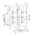
- FIG. 2A is a diagram showing a display driving circuit 2 according to a first embodiment of the invention. It includes a data driver 21 , a scan driver 22 , a pixel matrix composed of four (for example) display cells 231 ⁇ 234 , and two switches 241 and 242 .
- the data driver 21 outputs data signals for the display cells 231 ⁇ 234 through a data line 25 .
- the scan driver 22 outputs scan signals S 1 and S 2 through scan lines 261 and 262 .
- the display cells 231 and 233 commonly receive the scan signal S 1 through the scan line 261 , and the display cells 232 and 234 commonly receive the scan signal S 2 through the scan line 262 .
- the display cells 231 ⁇ 234 respectively receive the corresponding data signals commonly through the data line 25 .
- the switches 241 and 242 are respectively coupled between the data line 25 and the display cell 233 , and between the data line 25 and the display cell 234 .
- the display cells 231 and 232 in the odd columns of the pixel matrix are respectively composed of a transistor M 21 and a capacitor C 21 , and a transistor M 22 and C 22 .
- the transistor M 21 and M 22 have gates respectively coupled to the scan lines 261 and 262 , drains commonly coupled to the data line 25 , and sources coupled to the capacitors C 21 and C 22 .
- the display cells 233 and 234 in the even columns of the pixel matrix are respectively composed of a transistor M 23 and a capacitor C 23 , and a transistor M 24 and C 24 .
- the transistor M 23 and M 24 have gates respectively coupled to the scan lines 261 and 262 , drains respectively coupled to the switches 241 and 242 , and sources coupled to the capacitors C 23 and C 24 .
- the switches 241 and 242 are transistors M 25 and M 26 respectively.
- the transistors M 25 and M 26 have gates coupled to receive a signal Swing and drains coupled to the data line 25 .
- FIG. 2B is a diagram showing signal timing of the driving circuit in FIG. 2A.
- the scan period when the scan signal S 1 is asserted (has a logic high level) is divided into two sub-periods T1 and T2.
- the signal Swing is asserted (has a logic high level) and turns on the transistor M 25 (closes the switch 241 ).
- the display cell 233 in the even column of the pixel matrix receives the data signal from the data driver 21 through the data line 25 .
- the transistor M 25 is turned off (the switch 241 is opened) by the signal Swing.
- the display cell 231 in the odd column of the pixel matrix receives the data signal from the data driver 21 through the data line 25 . It is noted that although the display cell 231 also receives the data signal for the display cell 233 during the period T1, it is refreshed by the data signal received during the period T2.
- the next scan period when the scan signal S 2 is asserted (has a logic high level) is divided into two sub-periods T3 and T4.
- the signal Swing is asserted (has a logic high level) and turns on the transistor M 26 (closes the switch 242 ).
- the display cell 234 in the even column of the pixel matrix receives the data signal from the data driver 21 through the data line 25 .
- the transistor M 26 is turned off (the switch 242 is opened) by the signal Swing.
- the display cell 232 in the odd column of the pixel matrix receives the data signal from the data driver 21 through the data line 25 . It is noted that although the display cell 232 also receives the data signal for the display cell 234 during the period T3, it is refreshed by the data signal received during the period T4.
- FIG. 3A is a diagram showing a display driving circuit 3 according to a second embodiment of the invention. It includes a data driver 31 , a scan driver 32 , a pixel matrix composed of four (for example) display cells 331 ⁇ 334 , and two switches 341 and 342 .
- the data driver 31 outputs data signals for the display cells 231 ⁇ 234 through a data line 35 .
- the scan driver 32 outputs scan signals S 1 and S 2 through scan lines 361 and 362 .
- the display cells 331 and 333 commonly receive the scan signal S 1 through the scan line 361
- the display cells 332 and 334 commonly receive the scan signal S 2 through the scan line 362 .
- the display cells 331 and 332 respectively receive the corresponding data signals commonly through the data line 35 .
- the display cells 333 and 334 respectively receive the corresponding data signals via the switches 341 and 342 .
- the switches 341 and 342 are respectively coupled between the data line 35 and the display cell 333 , and between the data line 35 and the display cell 334 .
- the display cells 331 and 332 in the odd columns of the pixel matrix are respectively composed of a transistor M 31 and a capacitor C 31 , and a transistor M 32 and C 32 .
- the transistor M 31 and M 32 have gates respectively coupled to the scan lines 361 and 362 , drains commonly coupled to the data line 35 , and sources coupled to the capacitors C 31 and C 32 .
- the display cells 333 and 334 in the even columns of the pixel matrix are respectively composed of a transistor M 33 and a capacitor C 33 , and a transistor M 34 and C 34 .
- the transistors M 33 and M 34 have gates respectively coupled to the scan lines 361 and 362 , drains respectively coupled to the switches 341 and 342 , and sources coupled to the capacitors C 33 and C 34 .
- the switches 341 and 342 are transistors M 35 and M 36 respectively.
- the transistor M 35 has a gate coupled to the scan line 362 and the transistor M 36 has a gate coupled to the scan line for the next row.
- FIG. 3B is a diagram showing signal timing of the driving circuit in FIG. 3A.
- the signal Swing is integrated into the scan signals S 1 and S 2 shown in FIG. 3B. That is to say, the scan driver 22 outputs the scan signal comprising the signal Swing.
- the signal S 1 respectively carries a logic high and low level controlling the switches in a previous row (not shown) of the pixel matrix.
- the signal S 2 stays at the logic low level. Therefore, the display cells 331 ⁇ 334 are not yet activated.
- the scan period when the scan signal S 1 is asserted (has a logic high level) is divided into two sub-periods T3 and T4, and the signal S 2 is used as the signal Swing for the switches 341 and 342 .
- the signal S 2 has a high logic level to turn on the transistor M 35 (closes the switch 341 ).
- the display cell 333 in the even column of the pixel matrix receives the data signal from the data driver 31 through the data line 35 .
- the transistor M 35 is turned off (the switch 341 is opened) by the signal S 2 .
- the display cell 331 in the odd column of the pixel matrix receives the data signal from the data driver 31 through the data line 35 . It is noted that although the display cell 331 also receives the data signal for the display cell 333 during the period T3, it is refreshed by the data signal received during the period T4.
- the next scan period when the scan signal 52 is asserted (has a logic high level) is divided into two sub-periods T5 and T6, the scan signal (not shown) for the display cells in the next row of the pixel matrix is used as the signal Swing.
- the transistors M 31 , M 35 , M 33 are turned off during the periods T5 and T6.
- the transistor M 36 is turned on(the switch 342 is closes) by the next scan signal.
- the display cell 334 in the even column of the pixel matrix receives the data signal from the data driver 31 through the data line 35 .
- the transistor M 36 is turned off (the switch 342 is opened) by the next scan signal.
- the display cell 332 in the odd column of the pixel matrix receives the data signal from the data driver 31 through the data line 35 . It is noted that although the display cell 332 also receives the data signal for the display cell 334 during the period T5, it is refreshed by the data signal received during the period T6.
- FIG. 4A is a diagram showing a display driving circuit 4 according to a third embodiment of the invention. It includes a data driver 41 , a scan driver 42 , a pixel matrix composed of four (for example) display cells 431 ⁇ 434 , and two switches 441 and 442 .
- the data driver 41 outputs data signals for the display cells 431 ⁇ 434 through a data line 45 .
- the scan driver 42 outputs scan signals S 3 and S 4 through scan lines 461 and 462 .
- the display cells 431 ⁇ 434 respectively receive the corresponding data signals commonly through the data line 45 .
- the display cells 433 and 434 receive a signal Swing via switches 441 and 442 respectively.
- the display cells 431 and 432 in the odd columns of the pixel matrix are respectively composed of a transistor M 41 and a capacitor C 41 , and a transistor M 42 and C 42 .
- the transistor M 41 and M 42 have gates respectively coupled to the scan lines 461 and 462 , drains commonly coupled to the data line 45 , and sources coupled to the capacitors C 41 and C 42 .
- the display cells 433 and 434 in the even columns of the pixel matrix are respectively composed of a transistor M 43 and a capacitor C 43 , and a transistor M 44 and C 44 .
- the transistor M 43 and M 44 have gates respectively coupled to the switches 441 and 442 , drains commonly coupled to the data line 45 , and sources coupled to the capacitors C 43 and C 44 .
- the switches 441 and 442 are transistors M 45 and M 46 respectively.
- the transistors M 45 and M 46 have gates respectively coupled to the scan lines 461 and 462 and drains coupled to receive the signal Swing.
- FIG. 4B is a diagram showing signal timing of the driving circuit in FIG. 4A.
- the scan period when the scan signal S 3 is asserted (has a logic high level) is divided into two sub-periods T1 and T2.
- the transistors M 41 and M 45 are turned on (the switches 441 is closed) during this scan period.
- the signal Swing is asserted (has a logic high level) and turns on the transistor M 43 .
- the display cell 433 in the even column of the pixel matrix receives the data signal from the data driver 41 through the data line 45 .
- the transistor M 43 is turned off by the signal Swing.
- the display cell 431 in the odd column of the pixel matrix receives the data signal from the data driver 41 through the data line 45 . It is noted that although the display cell 431 also receives the data signal for the display cell 433 during the period T1, it is refreshed by the data signal received during the period T2.
- the next scan period when the scan signal S 4 is asserted (has a logic high level) is divided into two sub-periods T3 and T4.
- the transistors M 42 and M 46 are turned on (the switches 442 are closed) during this scan period.
- the signal Swing is asserted (has a logic high level) and turns on the transistor M 4 .
- the display cell 434 in the even column of the pixel matrix receives the data signal from the data driver 41 through the data line 45 .
- the transistor M 44 is turned off by the signal Swing.
- the display cell 432 in the odd column of the pixel matrix receives the data signal from the data driver 41 through the data line 45 . It is noted that although the display cell 432 also receives the data signal for the display cell 434 during the period T3, it is refreshed by the data signal received during the period T4.
- FIG. 5A is a diagram showing a display driving circuit 5 according to a fourth embodiment of the invention. It includes a data driver 51 , a scan driver 52 , a pixel matrix composed of four (for example) display cells 531 ⁇ 534 , and two switches 541 and 542 .
- the data driver 51 outputs data signals for the display cells 531 ⁇ 534 through a data line 55 .
- the scan driver 52 outputs scan signals S 3 and S 4 through scan lines 561 and 562 .
- the display cells 531 ⁇ 534 respectively receive the corresponding data signals commonly through the data line 55 .
- the switches 541 and 542 are respectively coupled between the scan line 562 and the display cell 533 , and between the scan line for the display cells in the next row (not shown) of the pixel matrix and the display cell 534 .
- the display cells 531 and 532 in the odd columns of the pixel matrix are respectively composed of a transistor M 51 and a capacitor C 51 , and a transistor M 52 and C 52 .
- the transistor M 51 and M 52 have gates respectively coupled to the scan lines 561 and 562 , drains commonly coupled to the data line 55 , and sources coupled to the capacitors C 51 and C 52 .
- the display cells 533 and 534 in the even columns of the pixel matrix are respectively composed of a transistor M 53 and a capacitor C 53 , and a transistor M 54 and C 54 .
- the transistor M 53 and M 54 have gates respectively coupled to the switches 541 and 542 , drains commonly coupled to the data line 55 , and sources coupled to the capacitors C 53 and C 54 .
- the switches 541 and 542 are transistors M 55 and M 56 respectively.
- the transistors M 55 and M 56 has gates respectively coupled to the scan lines 561 and 562 to receive the scan signals S 3 and S 4 , and sources respectively coupled to the scan line 562 and the scan line for the next row.
- FIG. 5B is a diagram showing signal timing of the driving circuit in FIG. 5A.
- the signal Swing is integrated into the scan signals S 3 and S 4 shown in FIG. 5B. That is to say, the scan driver 52 outputs the scan signal comprising the signal Swing.
- the signal S 3 respectively carries a logic high and low level controlling the switches in a previous row (not shown) of the pixel matrix.
- the signal S 4 stays at the logic low level. Therefore, the display cells 531 ⁇ 534 are not yet activated.
- the scan period when the scan signal S 3 is asserted (has a logic high level) is divided into two sub-periods T3 and T4, and the signal S 4 is used as the signal Swing for the switches 541 and 542 .
- the transistors M 51 and M 55 are turned on (the switches 541 is closed) during this scan period.
- the signal S 4 has a high logic level to turn on the transistor M 53 .
- the display cell 533 in the even column of the pixel matrix receives the data signal from the data driver 51 through the data line 55 .
- the transistor M 53 is turned off by the signal S 4 .
- the display cell 531 in the odd column of the pixel matrix receives the data signal from the data driver 51 through the data line 55 . It is noted that although the display cell 531 also receives the data signal for the display cell 533 during the period T3, it is refreshed by the data signal received during the period T4.
- the next scan period when the scan signal S 4 is asserted (has a logic high level) is divided into two sub-periods T5 and T6, the scan signal (not shown) for the display cells in the next row of the pixel matrix is used as the signal Swing.
- the transistors M 52 and M 56 are turned on (the switches 542 is closed) during this scan period.
- the transistor M 54 is turned on by the next scan signal.
- the display cell 534 in the even column of the pixel matrix receives the data signal from the data driver 51 through the data line 55 .
- the transistor M 54 is turned off by the next scan signal.
- the display cell 532 in the odd column of the pixel matrix receives the data signal from the data driver 51 through the data line 55 . It is noted that although the display cell 532 also receives the data signal for the display cell 534 during the period T5, it is refreshed by the data signal received during the period T6.
- the present invention provides a display driving circuit with fewer data drivers.
- Each pair of display cells is equipped with a switch for data terminal sharing.
- the switching frequency of the switches is lowered to the frame rate, which eliminates the reliability issue in the conventional display driving circuit.
Landscapes
- Engineering & Computer Science (AREA)
- Physics & Mathematics (AREA)
- Computer Hardware Design (AREA)
- General Physics & Mathematics (AREA)
- Theoretical Computer Science (AREA)
- Control Of Indicators Other Than Cathode Ray Tubes (AREA)
- Liquid Crystal Display Device Control (AREA)
Abstract
Description
- 1. Field of the Invention
- The present invention relates to a display driving circuit and particularly to a display driving circuit with fewer data drivers.
- 2. Description of the Prior Art
- FIG. 1 is a diagram showing a conventional
display driving circuit 1. It includes twodata drivers scan driver 11, a pixel matrix composed ofdisplay cells 13, andswitches display cells 13 in the odd columns of the pixel matrix receives a data signal through adata line 151 from thedata driver display cells 13 in the even columns of the pixel matrix receives a data signal through adata line 152 from thedata driver display cells 13 also receive scan signals throughscan lines 14 from thescan driver 11. To reduce the number of the data drivers,data line display cells 13 in the odd and even column of the pixel matrix share the same data terminal as the data driver through theswitches display cells 13 in the scanned row of the matrix receive the data signal output from the same terminal of thedata driver - However, in the conventional display driving circuit, the switching frequency of the
switches display cells 13. This results in high current stress which degrades the reliability of the circuit. - The object of the present invention is to provide a display driving circuit with switches for data terminal sharing individually for each of display cells. This lowers the switching frequency of the switches.
- The present invention provides a display driving circuit comprising a data driver sequentially outputting a first, second, third and fourth data signal through a data line, a scan driver outputting a first and second scan signal through a first and second scan line respectively, a first, second, third and fourth display cell respectively receiving the first, second, third and fourth data signal through the data line, the first and second display cell commonly receiving the first scan signal through the first scan line, and the third and fourth display cell commonly receiving the second scan signal through the second scan line, and a first and second switch, the first switch electrically coupling the first display cell to the data line when the first scan and data signals are asserted, and electrically isolating the first display cell from the data line when the first scan and second data signals are asserted, and the second switch electrically coupling the third display cell to the data line when the second scan and third data signals are asserted, and electrically isolating the first display cell from the data line when the second scan and fourth data signals are asserted.
- The present invention provides another display driving circuit comprising a data driver sequentially outputting a first, second, third and fourth data signal through a data line, a scan driver outputting a first and second scan signal through a first and second scan line respectively, a first, second, third and fourth display cell respectively receiving the first, second, third and fourth data signal through the data line, the first and second display cell commonly receiving the first scan signal through the first scan line, and the third and fourth display cell commonly receiving the second scan signal through the second scan line, and a first and second switch, the first switch electrically coupling the first display cell to receive a swing signal when the first scan signal is asserted, wherein the swing signal is asserted to couple the first display cell to receive the first data signal when the first data signal is asserted, and the second switch electrically coupling the third display cell to receive the swing signal when the second scan signal is asserted, wherein the swing signal is asserted to couple the third display cell to receive the third data signal when the third data signal is asserted.
- The present invention provides still another display driving circuit comprising a data driver sequentially outputting a data signal through a data line, a scan driver outputting a scan signal through a scan line, a first transistor having a gate coupled to the scan line and a drain coupled to the data line, a second transistor having a gate coupled to receive a swing signal and a drain coupled to the data line, and being sequentially turned on and off by the swing signal when the scan signal is asserted, a third transistor having a gate coupled to the scan line and a drain coupled to a source of the second transistor, and a first and second capacitor respectively coupled to sources of the first and third transistor.
- The present invention further provides a display driving circuit comprising a data driver sequentially outputting a data signal through a data line, a scan driver outputting a scan signal through a scan line, a first transistor having a gate coupled to the scan line and a drain coupled to the data line, a second transistor having a drain coupled to the data line, a third transistor having a gate coupled to the scan line, a source coupled to a gate of the second transistor and a drain coupled to receive a swing signal, wherein when the scan signal is asserted, the third transistor is turned on to electrically couple the gate of the third transistor to receive the swing signal and the second transistor is sequentially turned on and off, and a first and second capacitor respectively coupled to the sources of the first and third transistor.
- Thus, in the present invention, each pair of display cells are equipped with a switch for data terminal sharing. The switching frequency of the switches is lowered to the frame rate, which eliminates the reliability issue in the conventional display driving circuit.
- The present invention will become more fully understood from the detailed description given hereinbelow and the accompanying drawings, given by way of illustration only and thus not intended to be limitative of the present invention.
- FIG. 1 is a diagram showing a conventional display driving circuit.
- FIGS. 2A and 2B are diagrams showing a display driving circuit and signal timing thereof according to a first embodiment of the invention.
- FIGS. 3A and 3B are diagrams showing a display driving circuit and signal timing thereof according to a second embodiment of the invention.
- FIGS. 4A and 4B are diagrams showing a display driving circuit and signal timing thereof according to a third embodiment of the invention.
- FIGS. 5A and 5B are diagrams showing a display driving circuit and signal timing thereof according to a fourth embodiment of the invention.
- FIG. 2A is a diagram showing a
display driving circuit 2 according to a first embodiment of the invention. It includes adata driver 21, ascan driver 22, a pixel matrix composed of four (for example)display cells 231˜234, and twoswitches data driver 21 outputs data signals for thedisplay cells 231˜234 through adata line 25. Thescan driver 22 outputs scan signals S1 and S2 throughscan lines display cells scan line 261, and thedisplay cells scan line 262. Thedisplay cells 231˜234 respectively receive the corresponding data signals commonly through thedata line 25. Theswitches data line 25 and thedisplay cell 233, and between thedata line 25 and thedisplay cell 234. - The
display cells scan lines data line 25, and sources coupled to the capacitors C21 and C22. Thedisplay cells scan lines switches switches data line 25. - FIG. 2B is a diagram showing signal timing of the driving circuit in FIG. 2A.
- The scan period when the scan signal S 1 is asserted (has a logic high level) is divided into two sub-periods T1 and T2. During the period T1, the signal Swing is asserted (has a logic high level) and turns on the transistor M25 (closes the switch 241). The
display cell 233 in the even column of the pixel matrix receives the data signal from thedata driver 21 through thedata line 25. During the period T2, the transistor M25 is turned off (theswitch 241 is opened) by the signal Swing. Thedisplay cell 231 in the odd column of the pixel matrix receives the data signal from thedata driver 21 through thedata line 25. It is noted that although thedisplay cell 231 also receives the data signal for thedisplay cell 233 during the period T1, it is refreshed by the data signal received during the period T2. - The next scan period when the scan signal S 2 is asserted (has a logic high level) is divided into two sub-periods T3 and T4. During the period T3, the signal Swing is asserted (has a logic high level) and turns on the transistor M26 (closes the switch 242). The
display cell 234 in the even column of the pixel matrix receives the data signal from thedata driver 21 through thedata line 25. During the period T4, the transistor M26 is turned off (theswitch 242 is opened) by the signal Swing. Thedisplay cell 232 in the odd column of the pixel matrix receives the data signal from thedata driver 21 through thedata line 25. It is noted that although thedisplay cell 232 also receives the data signal for thedisplay cell 234 during the period T3, it is refreshed by the data signal received during the period T4. - FIG. 3A is a diagram showing a
display driving circuit 3 according to a second embodiment of the invention. It includes adata driver 31, ascan driver 32, a pixel matrix composed of four (for example)display cells 331˜334, and twoswitches data driver 31 outputs data signals for thedisplay cells 231˜234 through adata line 35. Thescan driver 32 outputs scan signals S1 and S2 throughscan lines display cells scan line 361, and thedisplay cells scan line 362. Thedisplay cells data line 35. Thedisplay cells switches switches data line 35 and thedisplay cell 333, and between thedata line 35 and thedisplay cell 334. - The
display cells scan lines data line 35, and sources coupled to the capacitors C31 and C32. Thedisplay cells scan lines switches switches scan line 362 and the transistor M36 has a gate coupled to the scan line for the next row. - FIG. 3B is a diagram showing signal timing of the driving circuit in FIG. 3A. By comparing the signal timing shown in FIGS. 2B and 3B, it is noted that the signal Swing is integrated into the scan signals S 1 and S2 shown in FIG. 3B. That is to say, the
scan driver 22 outputs the scan signal comprising the signal Swing. - During periods T1 and T2, the signal S 1 respectively carries a logic high and low level controlling the switches in a previous row (not shown) of the pixel matrix. The signal S2 stays at the logic low level. Therefore, the
display cells 331˜334 are not yet activated. - The scan period when the scan signal S 1 is asserted (has a logic high level) is divided into two sub-periods T3 and T4, and the signal S2 is used as the signal Swing for the
switches display cell 333 in the even column of the pixel matrix receives the data signal from thedata driver 31 through thedata line 35. During the period T4, the transistor M35 is turned off (theswitch 341 is opened) by the signal S2. Thedisplay cell 331 in the odd column of the pixel matrix receives the data signal from thedata driver 31 through thedata line 35. It is noted that although thedisplay cell 331 also receives the data signal for thedisplay cell 333 during the period T3, it is refreshed by the data signal received during the period T4. - The next scan period when the
scan signal 52 is asserted (has a logic high level) is divided into two sub-periods T5 and T6, the scan signal (not shown) for the display cells in the next row of the pixel matrix is used as the signal Swing. The transistors M31, M35, M33 are turned off during the periods T5 and T6. During the period T5, the transistor M36 is turned on(theswitch 342 is closes) by the next scan signal. Thedisplay cell 334 in the even column of the pixel matrix receives the data signal from thedata driver 31 through thedata line 35. During the period T6, the transistor M36 is turned off (theswitch 342 is opened) by the next scan signal. Thedisplay cell 332 in the odd column of the pixel matrix receives the data signal from thedata driver 31 through thedata line 35. It is noted that although thedisplay cell 332 also receives the data signal for thedisplay cell 334 during the period T5, it is refreshed by the data signal received during the period T6. - FIG. 4A is a diagram showing a
display driving circuit 4 according to a third embodiment of the invention. It includes adata driver 41, a scan driver 42, a pixel matrix composed of four (for example)display cells 431˜434, and twoswitches data driver 41 outputs data signals for thedisplay cells 431˜434 through adata line 45. The scan driver 42 outputs scan signals S3 and S4 throughscan lines display cells 431˜434 respectively receive the corresponding data signals commonly through thedata line 45. Thedisplay cells switches - The
display cells scan lines data line 45, and sources coupled to the capacitors C41 and C42. Thedisplay cells switches data line 45, and sources coupled to the capacitors C43 and C44. Theswitches scan lines - FIG. 4B is a diagram showing signal timing of the driving circuit in FIG. 4A.
- The scan period when the scan signal S 3 is asserted (has a logic high level) is divided into two sub-periods T1 and T2. The transistors M41 and M45 are turned on (the
switches 441 is closed) during this scan period. During the period T1, the signal Swing is asserted (has a logic high level) and turns on the transistor M43. Thedisplay cell 433 in the even column of the pixel matrix receives the data signal from thedata driver 41 through thedata line 45. During the period T2, the transistor M43 is turned off by the signal Swing. Thedisplay cell 431 in the odd column of the pixel matrix receives the data signal from thedata driver 41 through thedata line 45. It is noted that although thedisplay cell 431 also receives the data signal for thedisplay cell 433 during the period T1, it is refreshed by the data signal received during the period T2. - The next scan period when the scan signal S 4 is asserted (has a logic high level) is divided into two sub-periods T3 and T4. The transistors M42 and M46 are turned on (the
switches 442 are closed) during this scan period. During the period T3, the signal Swing is asserted (has a logic high level) and turns on the transistor M4. Thedisplay cell 434 in the even column of the pixel matrix receives the data signal from thedata driver 41 through thedata line 45. During the period T4, the transistor M44 is turned off by the signal Swing. Thedisplay cell 432 in the odd column of the pixel matrix receives the data signal from thedata driver 41 through thedata line 45. It is noted that although thedisplay cell 432 also receives the data signal for thedisplay cell 434 during the period T3, it is refreshed by the data signal received during the period T4. - FIG. 5A is a diagram showing a
display driving circuit 5 according to a fourth embodiment of the invention. It includes adata driver 51, ascan driver 52, a pixel matrix composed of four (for example)display cells 531˜534, and twoswitches data driver 51 outputs data signals for thedisplay cells 531˜534 through adata line 55. Thescan driver 52 outputs scan signals S3 and S4 throughscan lines display cells 531˜534 respectively receive the corresponding data signals commonly through thedata line 55. Theswitches scan line 562 and thedisplay cell 533, and between the scan line for the display cells in the next row (not shown) of the pixel matrix and thedisplay cell 534. - The
display cells 531 and 532 in the odd columns of the pixel matrix are respectively composed of a transistor M51 and a capacitor C51, and a transistor M52 and C52. The transistor M51 and M52 have gates respectively coupled to thescan lines data line 55, and sources coupled to the capacitors C51 and C52. Thedisplay cells switches data line 55, and sources coupled to the capacitors C53 and C54. Theswitches scan lines scan line 562 and the scan line for the next row. - FIG. 5B is a diagram showing signal timing of the driving circuit in FIG. 5A. By comparing the signal timing shown in FIGS. 4B and 5B, it is noted that the signal Swing is integrated into the scan signals S 3 and S4 shown in FIG. 5B. That is to say, the
scan driver 52 outputs the scan signal comprising the signal Swing. - During periods T1 and T2, the signal S 3 respectively carries a logic high and low level controlling the switches in a previous row (not shown) of the pixel matrix. The signal S4 stays at the logic low level. Therefore, the
display cells 531˜534 are not yet activated. - The scan period when the scan signal S 3 is asserted (has a logic high level) is divided into two sub-periods T3 and T4, and the signal S4 is used as the signal Swing for the
switches switches 541 is closed) during this scan period. During the period T3, the signal S4 has a high logic level to turn on the transistor M53. Thedisplay cell 533 in the even column of the pixel matrix receives the data signal from thedata driver 51 through thedata line 55. During the period T4, the transistor M53 is turned off by the signal S4. Thedisplay cell 531 in the odd column of the pixel matrix receives the data signal from thedata driver 51 through thedata line 55. It is noted that although thedisplay cell 531 also receives the data signal for thedisplay cell 533 during the period T3, it is refreshed by the data signal received during the period T4. - The next scan period when the scan signal S 4 is asserted (has a logic high level) is divided into two sub-periods T5 and T6, the scan signal (not shown) for the display cells in the next row of the pixel matrix is used as the signal Swing. The transistors M52 and M56 are turned on (the
switches 542 is closed) during this scan period. During the period T5, the transistor M54 is turned on by the next scan signal. Thedisplay cell 534 in the even column of the pixel matrix receives the data signal from thedata driver 51 through thedata line 55. During the period T6, the transistor M54 is turned off by the next scan signal. The display cell 532 in the odd column of the pixel matrix receives the data signal from thedata driver 51 through thedata line 55. It is noted that although the display cell 532 also receives the data signal for thedisplay cell 534 during the period T5, it is refreshed by the data signal received during the period T6. - In conclusion, the present invention provides a display driving circuit with fewer data drivers. Each pair of display cells is equipped with a switch for data terminal sharing. Thus, the switching frequency of the switches is lowered to the frame rate, which eliminates the reliability issue in the conventional display driving circuit.
- The foregoing description of the preferred embodiments of this invention has been presented for purposes of illustration and description. Obvious modifications or variations are possible in light of the above teaching. The embodiments were chosen and described to provide the best illustration of the principles of this invention and its practical application to thereby enable those skilled in the art to utilize the invention in various embodiments and with various modifications as are suited to the particular use contemplated. All such modifications and variations are within the scope of the present invention as determined by the appended claims when interpreted in accordance with the breadth to which they are fairly, legally, and equitably entitled.
Claims (13)
Applications Claiming Priority (2)
| Application Number | Priority Date | Filing Date | Title |
|---|---|---|---|
| TW091107355A TW580665B (en) | 2002-04-11 | 2002-04-11 | Driving circuit of display |
| TW91107355 | 2002-04-11 |
Publications (2)
| Publication Number | Publication Date |
|---|---|
| US20030193490A1 true US20030193490A1 (en) | 2003-10-16 |
| US7102630B2 US7102630B2 (en) | 2006-09-05 |
Family
ID=28788592
Family Applications (1)
| Application Number | Title | Priority Date | Filing Date |
|---|---|---|---|
| US10/411,935 Expired - Lifetime US7102630B2 (en) | 2002-04-11 | 2003-04-11 | Display driving circuit |
Country Status (2)
| Country | Link |
|---|---|
| US (1) | US7102630B2 (en) |
| TW (1) | TW580665B (en) |
Cited By (12)
| Publication number | Priority date | Publication date | Assignee | Title |
|---|---|---|---|---|
| US20070001938A1 (en) * | 2005-06-30 | 2007-01-04 | Lg Philips Lcd Co., Ltd. | Display device and driving method |
| US20070070017A1 (en) * | 2005-09-26 | 2007-03-29 | Au Optronics Corp. | Display panels |
| US20070222736A1 (en) * | 2006-03-23 | 2007-09-27 | Au Optronics Corp. | Method of driving liquid crystal display panel |
| US20080001863A1 (en) * | 2006-06-30 | 2008-01-03 | Lg. Philips Lcd Co., Ltd. | Organic light emitting diode display and driving method thereof |
| CN100365681C (en) * | 2005-10-12 | 2008-01-30 | 友达光电股份有限公司 | Display panel, related electronic device and driving method |
| US20080030439A1 (en) * | 2006-08-01 | 2008-02-07 | Dong-Yong Shin | Organic light emitting display device |
| US20080123002A1 (en) * | 2006-11-27 | 2008-05-29 | Innolux Display Corp. | Liquid crystal display and driving method thereof |
| US20090322730A1 (en) * | 2008-06-25 | 2009-12-31 | Sony Corporation | Display device |
| CN102023401A (en) * | 2009-09-18 | 2011-04-20 | 北京京东方光电科技有限公司 | TFT-LCD array substrate and method for manufacturing the same |
| CN102446497A (en) * | 2010-09-30 | 2012-05-09 | 北京京东方光电科技有限公司 | Array substrate and driving method therefor |
| TWI421849B (en) * | 2010-12-30 | 2014-01-01 | Au Optronics Corp | Liquid crystal display device |
| CN117130196A (en) * | 2023-08-30 | 2023-11-28 | 重庆惠科金渝光电科技有限公司 | Array substrate and display device |
Families Citing this family (1)
| Publication number | Priority date | Publication date | Assignee | Title |
|---|---|---|---|---|
| CN106019743B (en) * | 2016-06-15 | 2023-08-22 | 京东方科技集团股份有限公司 | An array substrate, its driving method and related device |
Citations (7)
| Publication number | Priority date | Publication date | Assignee | Title |
|---|---|---|---|---|
| US4873516A (en) * | 1987-06-01 | 1989-10-10 | General Electric Company | Method and system for eliminating cross-talk in thin film transistor matrix addressed liquid crystal displays |
| US5253091A (en) * | 1990-07-09 | 1993-10-12 | International Business Machines Corporation | Liquid crystal display having reduced flicker |
| US6011534A (en) * | 1995-10-05 | 2000-01-04 | Sharp Kabushiki Kaisha | Driving circuit for image display device including signal generator which generates at least two types of sampling pulse timing signals having phases that differ from each other |
| US6011531A (en) * | 1996-10-21 | 2000-01-04 | Xerox Corporation | Methods and applications of combining pixels to the gate and data lines for 2-D imaging and display arrays |
| US6593905B1 (en) * | 2000-08-08 | 2003-07-15 | Au Optronics Corp. | Liquid crystal display panel and the control method thereof |
| US6646637B1 (en) * | 2000-02-29 | 2003-11-11 | Hitachi, Ltd. | Liquid crystal display device |
| US6933910B2 (en) * | 2000-12-07 | 2005-08-23 | International Business Machines Corporation | Image display device and method thereof |
Family Cites Families (1)
| Publication number | Priority date | Publication date | Assignee | Title |
|---|---|---|---|---|
| US5313222A (en) * | 1992-12-24 | 1994-05-17 | Yuen Foong Yu H. K. Co., Ltd. | Select driver circuit for an LCD display |
-
2002
- 2002-04-11 TW TW091107355A patent/TW580665B/en not_active IP Right Cessation
-
2003
- 2003-04-11 US US10/411,935 patent/US7102630B2/en not_active Expired - Lifetime
Patent Citations (7)
| Publication number | Priority date | Publication date | Assignee | Title |
|---|---|---|---|---|
| US4873516A (en) * | 1987-06-01 | 1989-10-10 | General Electric Company | Method and system for eliminating cross-talk in thin film transistor matrix addressed liquid crystal displays |
| US5253091A (en) * | 1990-07-09 | 1993-10-12 | International Business Machines Corporation | Liquid crystal display having reduced flicker |
| US6011534A (en) * | 1995-10-05 | 2000-01-04 | Sharp Kabushiki Kaisha | Driving circuit for image display device including signal generator which generates at least two types of sampling pulse timing signals having phases that differ from each other |
| US6011531A (en) * | 1996-10-21 | 2000-01-04 | Xerox Corporation | Methods and applications of combining pixels to the gate and data lines for 2-D imaging and display arrays |
| US6646637B1 (en) * | 2000-02-29 | 2003-11-11 | Hitachi, Ltd. | Liquid crystal display device |
| US6593905B1 (en) * | 2000-08-08 | 2003-07-15 | Au Optronics Corp. | Liquid crystal display panel and the control method thereof |
| US6933910B2 (en) * | 2000-12-07 | 2005-08-23 | International Business Machines Corporation | Image display device and method thereof |
Cited By (19)
| Publication number | Priority date | Publication date | Assignee | Title |
|---|---|---|---|---|
| US7656368B2 (en) * | 2005-06-30 | 2010-02-02 | Lg Display Co., Ltd. | Display device and driving method |
| US20070001938A1 (en) * | 2005-06-30 | 2007-01-04 | Lg Philips Lcd Co., Ltd. | Display device and driving method |
| US20070070017A1 (en) * | 2005-09-26 | 2007-03-29 | Au Optronics Corp. | Display panels |
| US20100164917A1 (en) * | 2005-09-26 | 2010-07-01 | Au Optronics Corp. | Display panels |
| US7705840B2 (en) * | 2005-09-26 | 2010-04-27 | Au Optronics Corp. | Display panels |
| CN100365681C (en) * | 2005-10-12 | 2008-01-30 | 友达光电股份有限公司 | Display panel, related electronic device and driving method |
| US7714823B2 (en) | 2006-03-23 | 2010-05-11 | Au Optronics Corp. | Method of driving liquid crystal display panel |
| US20070222736A1 (en) * | 2006-03-23 | 2007-09-27 | Au Optronics Corp. | Method of driving liquid crystal display panel |
| US8139002B2 (en) * | 2006-06-30 | 2012-03-20 | Lg Display Co., Ltd. | Organic light emitting diode display and driving method thereof |
| US20080001863A1 (en) * | 2006-06-30 | 2008-01-03 | Lg. Philips Lcd Co., Ltd. | Organic light emitting diode display and driving method thereof |
| US7825881B2 (en) * | 2006-08-01 | 2010-11-02 | Samsung Mobile Display Co., Ltd. | Organic light emitting display device |
| US20080030439A1 (en) * | 2006-08-01 | 2008-02-07 | Dong-Yong Shin | Organic light emitting display device |
| US20080123002A1 (en) * | 2006-11-27 | 2008-05-29 | Innolux Display Corp. | Liquid crystal display and driving method thereof |
| US20090322730A1 (en) * | 2008-06-25 | 2009-12-31 | Sony Corporation | Display device |
| US8830149B2 (en) * | 2008-06-25 | 2014-09-09 | Sony Corporation | Display device |
| CN102023401A (en) * | 2009-09-18 | 2011-04-20 | 北京京东方光电科技有限公司 | TFT-LCD array substrate and method for manufacturing the same |
| CN102446497A (en) * | 2010-09-30 | 2012-05-09 | 北京京东方光电科技有限公司 | Array substrate and driving method therefor |
| TWI421849B (en) * | 2010-12-30 | 2014-01-01 | Au Optronics Corp | Liquid crystal display device |
| CN117130196A (en) * | 2023-08-30 | 2023-11-28 | 重庆惠科金渝光电科技有限公司 | Array substrate and display device |
Also Published As
| Publication number | Publication date |
|---|---|
| TW580665B (en) | 2004-03-21 |
| US7102630B2 (en) | 2006-09-05 |
Similar Documents
| Publication | Publication Date | Title |
|---|---|---|
| US7916114B2 (en) | Shift register units, display panels utilizing the same, and methods for improving current leakage thereof | |
| US6836269B2 (en) | Precharge circuit and image display device using the same | |
| US7233308B2 (en) | Shift register | |
| US8159486B2 (en) | Level converter circuit and a liquid crystal display device employing the same | |
| US6897847B2 (en) | Peripheral driver circuit of liquid crystal electro-optical device | |
| US9147370B2 (en) | Image display apparatus | |
| US7102630B2 (en) | Display driving circuit | |
| JP2001506044A (en) | Two-way shift register | |
| JPH08101669A (en) | Display device drive circuit | |
| RU2438194C1 (en) | Storage capacitor line drive circuit and display device | |
| KR20040053639A (en) | Device of driving display device | |
| US6275210B1 (en) | Liquid crystal display device and driver circuit thereof | |
| US20100164917A1 (en) | Display panels | |
| US20050236650A1 (en) | Array device with switching circuits bootstrap capacitors | |
| US6157228A (en) | Data line driving circuit formed by a TFT based on polycrystalline silicon | |
| US20040041801A1 (en) | Da converting circuit, display using the same, and mobile terminal having the display | |
| US20190197938A1 (en) | Liquid crystal display apparatus | |
| JPH07235844A (en) | Output buffer circuit for analog driver ic | |
| US10777161B2 (en) | Array substrate, liquid crystal display panel and display device | |
| US20050024317A1 (en) | Display device | |
| US20070153967A1 (en) | Dynamic shift register with built-in disable circuit | |
| US7830352B2 (en) | Driving circuit for flat panel display which provides a horizontal start signal to first and second shift register cells | |
| US20060208996A1 (en) | Semiconductor circuit | |
| JP2004350261A (en) | Sampling circuit and liquid crystal display including it | |
| US6956552B2 (en) | Method and apparatus for driving a display |
Legal Events
| Date | Code | Title | Description |
|---|---|---|---|
| AS | Assignment |
Owner name: AU OPTRONICS CORP., TAIWAN Free format text: ASSIGNMENT OF ASSIGNORS INTEREST;ASSIGNORS:LIU, BIING-DER;WONG, JIA-FAM;HSIEH, YAO-JEN;REEL/FRAME:013979/0756 Effective date: 20030401 |
|
| STCF | Information on status: patent grant |
Free format text: PATENTED CASE |
|
| CC | Certificate of correction | ||
| FEPP | Fee payment procedure |
Free format text: PAYOR NUMBER ASSIGNED (ORIGINAL EVENT CODE: ASPN); ENTITY STATUS OF PATENT OWNER: LARGE ENTITY |
|
| FPAY | Fee payment |
Year of fee payment: 4 |
|
| FPAY | Fee payment |
Year of fee payment: 8 |
|
| MAFP | Maintenance fee payment |
Free format text: PAYMENT OF MAINTENANCE FEE, 12TH YEAR, LARGE ENTITY (ORIGINAL EVENT CODE: M1553) Year of fee payment: 12 |