US6630699B1 - Transistor device having an isolation structure located under a source region, drain region and channel region and a method of manufacture thereof - Google Patents
Transistor device having an isolation structure located under a source region, drain region and channel region and a method of manufacture thereof Download PDFInfo
- Publication number
- US6630699B1 US6630699B1 US09/653,531 US65353100A US6630699B1 US 6630699 B1 US6630699 B1 US 6630699B1 US 65353100 A US65353100 A US 65353100A US 6630699 B1 US6630699 B1 US 6630699B1
- Authority
- US
- United States
- Prior art keywords
- region
- recited
- transistor device
- gate
- trench
- Prior art date
- Legal status (The legal status is an assumption and is not a legal conclusion. Google has not performed a legal analysis and makes no representation as to the accuracy of the status listed.)
- Expired - Lifetime
Links
- 238000002955 isolation Methods 0.000 title claims 3
- 238000000034 method Methods 0.000 title description 25
- 238000004519 manufacturing process Methods 0.000 title description 13
- 239000004065 semiconductor Substances 0.000 claims abstract description 38
- 239000000758 substrate Substances 0.000 claims abstract description 29
- 125000006850 spacer group Chemical group 0.000 claims description 33
- 239000007943 implant Substances 0.000 claims description 14
- 229910044991 metal oxide Inorganic materials 0.000 claims description 9
- 150000004706 metal oxides Chemical class 0.000 claims description 9
- 229910052710 silicon Inorganic materials 0.000 claims description 7
- 239000010703 silicon Substances 0.000 claims description 7
- 230000000295 complement effect Effects 0.000 claims description 3
- 230000015572 biosynthetic process Effects 0.000 description 37
- 239000002019 doping agent Substances 0.000 description 25
- 230000008569 process Effects 0.000 description 19
- 150000004767 nitrides Chemical class 0.000 description 11
- 238000000151 deposition Methods 0.000 description 8
- 230000003071 parasitic effect Effects 0.000 description 8
- 239000000463 material Substances 0.000 description 7
- 230000003647 oxidation Effects 0.000 description 6
- 238000007254 oxidation reaction Methods 0.000 description 6
- XUIMIQQOPSSXEZ-UHFFFAOYSA-N Silicon Chemical compound [Si] XUIMIQQOPSSXEZ-UHFFFAOYSA-N 0.000 description 5
- 238000005229 chemical vapour deposition Methods 0.000 description 5
- 229920002120 photoresistant polymer Polymers 0.000 description 5
- 238000004891 communication Methods 0.000 description 4
- 230000008021 deposition Effects 0.000 description 4
- 238000000059 patterning Methods 0.000 description 4
- 239000000126 substance Substances 0.000 description 4
- 238000009279 wet oxidation reaction Methods 0.000 description 4
- 238000001465 metallisation Methods 0.000 description 3
- 238000012856 packing Methods 0.000 description 3
- XYFCBTPGUUZFHI-UHFFFAOYSA-N Phosphine Chemical compound P XYFCBTPGUUZFHI-UHFFFAOYSA-N 0.000 description 2
- 230000008878 coupling Effects 0.000 description 2
- 238000010168 coupling process Methods 0.000 description 2
- 238000005859 coupling reaction Methods 0.000 description 2
- 238000005530 etching Methods 0.000 description 2
- 239000011521 glass Substances 0.000 description 2
- 229910021421 monocrystalline silicon Inorganic materials 0.000 description 2
- 238000012545 processing Methods 0.000 description 2
- 238000010561 standard procedure Methods 0.000 description 2
- 229910052581 Si3N4 Inorganic materials 0.000 description 1
- BLRPTPMANUNPDV-UHFFFAOYSA-N Silane Chemical compound [SiH4] BLRPTPMANUNPDV-UHFFFAOYSA-N 0.000 description 1
- 230000004075 alteration Effects 0.000 description 1
- 238000013459 approach Methods 0.000 description 1
- 238000004140 cleaning Methods 0.000 description 1
- 238000010276 construction Methods 0.000 description 1
- 238000007796 conventional method Methods 0.000 description 1
- 239000013078 crystal Substances 0.000 description 1
- 230000003247 decreasing effect Effects 0.000 description 1
- 230000007812 deficiency Effects 0.000 description 1
- 238000005137 deposition process Methods 0.000 description 1
- 238000013461 design Methods 0.000 description 1
- 230000009977 dual effect Effects 0.000 description 1
- 230000005684 electric field Effects 0.000 description 1
- 238000005516 engineering process Methods 0.000 description 1
- 238000000407 epitaxy Methods 0.000 description 1
- 230000006872 improvement Effects 0.000 description 1
- 239000012212 insulator Substances 0.000 description 1
- 230000010354 integration Effects 0.000 description 1
- 230000000873 masking effect Effects 0.000 description 1
- 230000007246 mechanism Effects 0.000 description 1
- 239000002184 metal Substances 0.000 description 1
- 229910000073 phosphorus hydride Inorganic materials 0.000 description 1
- 230000001902 propagating effect Effects 0.000 description 1
- 229910000077 silane Inorganic materials 0.000 description 1
- HQVNEWCFYHHQES-UHFFFAOYSA-N silicon nitride Chemical compound N12[Si]34N5[Si]62N3[Si]51N64 HQVNEWCFYHHQES-UHFFFAOYSA-N 0.000 description 1
- 238000006467 substitution reaction Methods 0.000 description 1
Images


Classifications
-
- H—ELECTRICITY
- H01—ELECTRIC ELEMENTS
- H01L—SEMICONDUCTOR DEVICES NOT COVERED BY CLASS H10
- H01L29/00—Semiconductor devices adapted for rectifying, amplifying, oscillating or switching, or capacitors or resistors with at least one potential-jump barrier or surface barrier, e.g. PN junction depletion layer or carrier concentration layer; Details of semiconductor bodies or of electrodes thereof ; Multistep manufacturing processes therefor
- H01L29/66—Types of semiconductor device ; Multistep manufacturing processes therefor
- H01L29/68—Types of semiconductor device ; Multistep manufacturing processes therefor controllable by only the electric current supplied, or only the electric potential applied, to an electrode which does not carry the current to be rectified, amplified or switched
- H01L29/76—Unipolar devices, e.g. field effect transistors
- H01L29/772—Field effect transistors
- H01L29/78—Field effect transistors with field effect produced by an insulated gate
- H01L29/785—Field effect transistors with field effect produced by an insulated gate having a channel with a horizontal current flow in a vertical sidewall of a semiconductor body, e.g. FinFET, MuGFET
-
- H—ELECTRICITY
- H01—ELECTRIC ELEMENTS
- H01L—SEMICONDUCTOR DEVICES NOT COVERED BY CLASS H10
- H01L21/00—Processes or apparatus adapted for the manufacture or treatment of semiconductor or solid state devices or of parts thereof
- H01L21/70—Manufacture or treatment of devices consisting of a plurality of solid state components formed in or on a common substrate or of parts thereof; Manufacture of integrated circuit devices or of parts thereof
- H01L21/71—Manufacture of specific parts of devices defined in group H01L21/70
- H01L21/76—Making of isolation regions between components
- H01L21/762—Dielectric regions, e.g. EPIC dielectric isolation, LOCOS; Trench refilling techniques, SOI technology, use of channel stoppers
- H01L21/7624—Dielectric regions, e.g. EPIC dielectric isolation, LOCOS; Trench refilling techniques, SOI technology, use of channel stoppers using semiconductor on insulator [SOI] technology
- H01L21/76264—SOI together with lateral isolation, e.g. using local oxidation of silicon, or dielectric or polycristalline material refilled trench or air gap isolation regions, e.g. completely isolated semiconductor islands
-
- H—ELECTRICITY
- H01—ELECTRIC ELEMENTS
- H01L—SEMICONDUCTOR DEVICES NOT COVERED BY CLASS H10
- H01L27/00—Devices consisting of a plurality of semiconductor or other solid-state components formed in or on a common substrate
- H01L27/02—Devices consisting of a plurality of semiconductor or other solid-state components formed in or on a common substrate including semiconductor components specially adapted for rectifying, oscillating, amplifying or switching and having at least one potential-jump barrier or surface barrier; including integrated passive circuit elements with at least one potential-jump barrier or surface barrier
- H01L27/12—Devices consisting of a plurality of semiconductor or other solid-state components formed in or on a common substrate including semiconductor components specially adapted for rectifying, oscillating, amplifying or switching and having at least one potential-jump barrier or surface barrier; including integrated passive circuit elements with at least one potential-jump barrier or surface barrier the substrate being other than a semiconductor body, e.g. an insulating body
- H01L27/1203—Devices consisting of a plurality of semiconductor or other solid-state components formed in or on a common substrate including semiconductor components specially adapted for rectifying, oscillating, amplifying or switching and having at least one potential-jump barrier or surface barrier; including integrated passive circuit elements with at least one potential-jump barrier or surface barrier the substrate being other than a semiconductor body, e.g. an insulating body the substrate comprising an insulating body on a semiconductor body, e.g. SOI
-
- H—ELECTRICITY
- H01—ELECTRIC ELEMENTS
- H01L—SEMICONDUCTOR DEVICES NOT COVERED BY CLASS H10
- H01L29/00—Semiconductor devices adapted for rectifying, amplifying, oscillating or switching, or capacitors or resistors with at least one potential-jump barrier or surface barrier, e.g. PN junction depletion layer or carrier concentration layer; Details of semiconductor bodies or of electrodes thereof ; Multistep manufacturing processes therefor
- H01L29/02—Semiconductor bodies ; Multistep manufacturing processes therefor
- H01L29/06—Semiconductor bodies ; Multistep manufacturing processes therefor characterised by their shape; characterised by the shapes, relative sizes, or dispositions of the semiconductor regions ; characterised by the concentration or distribution of impurities within semiconductor regions
- H01L29/0603—Semiconductor bodies ; Multistep manufacturing processes therefor characterised by their shape; characterised by the shapes, relative sizes, or dispositions of the semiconductor regions ; characterised by the concentration or distribution of impurities within semiconductor regions characterised by particular constructional design considerations, e.g. for preventing surface leakage, for controlling electric field concentration or for internal isolations regions
- H01L29/0642—Isolation within the component, i.e. internal isolation
- H01L29/0649—Dielectric regions, e.g. SiO2 regions, air gaps
- H01L29/0653—Dielectric regions, e.g. SiO2 regions, air gaps adjoining the input or output region of a field-effect device, e.g. the source or drain region
-
- H—ELECTRICITY
- H01—ELECTRIC ELEMENTS
- H01L—SEMICONDUCTOR DEVICES NOT COVERED BY CLASS H10
- H01L29/00—Semiconductor devices adapted for rectifying, amplifying, oscillating or switching, or capacitors or resistors with at least one potential-jump barrier or surface barrier, e.g. PN junction depletion layer or carrier concentration layer; Details of semiconductor bodies or of electrodes thereof ; Multistep manufacturing processes therefor
- H01L29/66—Types of semiconductor device ; Multistep manufacturing processes therefor
- H01L29/66007—Multistep manufacturing processes
- H01L29/66075—Multistep manufacturing processes of devices having semiconductor bodies comprising group 14 or group 13/15 materials
- H01L29/66227—Multistep manufacturing processes of devices having semiconductor bodies comprising group 14 or group 13/15 materials the devices being controllable only by the electric current supplied or the electric potential applied, to an electrode which does not carry the current to be rectified, amplified or switched, e.g. three-terminal devices
- H01L29/66409—Unipolar field-effect transistors
- H01L29/66477—Unipolar field-effect transistors with an insulated gate, i.e. MISFET
- H01L29/66742—Thin film unipolar transistors
- H01L29/66772—Monocristalline silicon transistors on insulating substrates, e.g. quartz substrates
-
- H—ELECTRICITY
- H01—ELECTRIC ELEMENTS
- H01L—SEMICONDUCTOR DEVICES NOT COVERED BY CLASS H10
- H01L29/00—Semiconductor devices adapted for rectifying, amplifying, oscillating or switching, or capacitors or resistors with at least one potential-jump barrier or surface barrier, e.g. PN junction depletion layer or carrier concentration layer; Details of semiconductor bodies or of electrodes thereof ; Multistep manufacturing processes therefor
- H01L29/66—Types of semiconductor device ; Multistep manufacturing processes therefor
- H01L29/68—Types of semiconductor device ; Multistep manufacturing processes therefor controllable by only the electric current supplied, or only the electric potential applied, to an electrode which does not carry the current to be rectified, amplified or switched
- H01L29/76—Unipolar devices, e.g. field effect transistors
- H01L29/772—Field effect transistors
- H01L29/78—Field effect transistors with field effect produced by an insulated gate
- H01L29/786—Thin film transistors, i.e. transistors with a channel being at least partly a thin film
- H01L29/78606—Thin film transistors, i.e. transistors with a channel being at least partly a thin film with supplementary region or layer in the thin film or in the insulated bulk substrate supporting it for controlling or increasing the safety of the device
- H01L29/78618—Thin film transistors, i.e. transistors with a channel being at least partly a thin film with supplementary region or layer in the thin film or in the insulated bulk substrate supporting it for controlling or increasing the safety of the device characterised by the drain or the source properties, e.g. the doping structure, the composition, the sectional shape or the contact structure
- H01L29/78621—Thin film transistors, i.e. transistors with a channel being at least partly a thin film with supplementary region or layer in the thin film or in the insulated bulk substrate supporting it for controlling or increasing the safety of the device characterised by the drain or the source properties, e.g. the doping structure, the composition, the sectional shape or the contact structure with LDD structure or an extension or an offset region or characterised by the doping profile
-
- H—ELECTRICITY
- H01—ELECTRIC ELEMENTS
- H01L—SEMICONDUCTOR DEVICES NOT COVERED BY CLASS H10
- H01L29/00—Semiconductor devices adapted for rectifying, amplifying, oscillating or switching, or capacitors or resistors with at least one potential-jump barrier or surface barrier, e.g. PN junction depletion layer or carrier concentration layer; Details of semiconductor bodies or of electrodes thereof ; Multistep manufacturing processes therefor
- H01L29/66—Types of semiconductor device ; Multistep manufacturing processes therefor
- H01L29/68—Types of semiconductor device ; Multistep manufacturing processes therefor controllable by only the electric current supplied, or only the electric potential applied, to an electrode which does not carry the current to be rectified, amplified or switched
- H01L29/76—Unipolar devices, e.g. field effect transistors
- H01L29/772—Field effect transistors
- H01L29/78—Field effect transistors with field effect produced by an insulated gate
- H01L29/786—Thin film transistors, i.e. transistors with a channel being at least partly a thin film
- H01L29/78606—Thin film transistors, i.e. transistors with a channel being at least partly a thin film with supplementary region or layer in the thin film or in the insulated bulk substrate supporting it for controlling or increasing the safety of the device
- H01L29/78639—Thin film transistors, i.e. transistors with a channel being at least partly a thin film with supplementary region or layer in the thin film or in the insulated bulk substrate supporting it for controlling or increasing the safety of the device with a drain or source connected to a bulk conducting substrate
-
- H—ELECTRICITY
- H01—ELECTRIC ELEMENTS
- H01L—SEMICONDUCTOR DEVICES NOT COVERED BY CLASS H10
- H01L21/00—Processes or apparatus adapted for the manufacture or treatment of semiconductor or solid state devices or of parts thereof
- H01L21/70—Manufacture or treatment of devices consisting of a plurality of solid state components formed in or on a common substrate or of parts thereof; Manufacture of integrated circuit devices or of parts thereof
- H01L21/71—Manufacture of specific parts of devices defined in group H01L21/70
- H01L21/76—Making of isolation regions between components
- H01L21/762—Dielectric regions, e.g. EPIC dielectric isolation, LOCOS; Trench refilling techniques, SOI technology, use of channel stoppers
- H01L21/7624—Dielectric regions, e.g. EPIC dielectric isolation, LOCOS; Trench refilling techniques, SOI technology, use of channel stoppers using semiconductor on insulator [SOI] technology
- H01L21/76264—SOI together with lateral isolation, e.g. using local oxidation of silicon, or dielectric or polycristalline material refilled trench or air gap isolation regions, e.g. completely isolated semiconductor islands
- H01L21/76278—Vertical isolation by selective deposition of single crystal silicon, i.e. SEG techniques
-
- H—ELECTRICITY
- H01—ELECTRIC ELEMENTS
- H01L—SEMICONDUCTOR DEVICES NOT COVERED BY CLASS H10
- H01L21/00—Processes or apparatus adapted for the manufacture or treatment of semiconductor or solid state devices or of parts thereof
- H01L21/70—Manufacture or treatment of devices consisting of a plurality of solid state components formed in or on a common substrate or of parts thereof; Manufacture of integrated circuit devices or of parts thereof
- H01L21/71—Manufacture of specific parts of devices defined in group H01L21/70
- H01L21/76—Making of isolation regions between components
- H01L21/762—Dielectric regions, e.g. EPIC dielectric isolation, LOCOS; Trench refilling techniques, SOI technology, use of channel stoppers
- H01L21/7624—Dielectric regions, e.g. EPIC dielectric isolation, LOCOS; Trench refilling techniques, SOI technology, use of channel stoppers using semiconductor on insulator [SOI] technology
- H01L21/76264—SOI together with lateral isolation, e.g. using local oxidation of silicon, or dielectric or polycristalline material refilled trench or air gap isolation regions, e.g. completely isolated semiconductor islands
- H01L21/76283—Lateral isolation by refilling of trenches with dielectric material
-
- H—ELECTRICITY
- H01—ELECTRIC ELEMENTS
- H01L—SEMICONDUCTOR DEVICES NOT COVERED BY CLASS H10
- H01L21/00—Processes or apparatus adapted for the manufacture or treatment of semiconductor or solid state devices or of parts thereof
- H01L21/70—Manufacture or treatment of devices consisting of a plurality of solid state components formed in or on a common substrate or of parts thereof; Manufacture of integrated circuit devices or of parts thereof
- H01L21/77—Manufacture or treatment of devices consisting of a plurality of solid state components or integrated circuits formed in, or on, a common substrate
- H01L21/78—Manufacture or treatment of devices consisting of a plurality of solid state components or integrated circuits formed in, or on, a common substrate with subsequent division of the substrate into plural individual devices
- H01L21/82—Manufacture or treatment of devices consisting of a plurality of solid state components or integrated circuits formed in, or on, a common substrate with subsequent division of the substrate into plural individual devices to produce devices, e.g. integrated circuits, each consisting of a plurality of components
- H01L21/84—Manufacture or treatment of devices consisting of a plurality of solid state components or integrated circuits formed in, or on, a common substrate with subsequent division of the substrate into plural individual devices to produce devices, e.g. integrated circuits, each consisting of a plurality of components the substrate being other than a semiconductor body, e.g. being an insulating body
Definitions
- the present invention is directed, in general, to a transistor device and, more specifically, to a transistor device having a dielectric region located under and in contact with a source region, a drain region and a channel region.
- One such challenge is that of eliminating parasitic capacitance as much as possible.
- the time delay of signals propagating through the transistor are heavily influenced by the various parasitic capacitances inevitably associated with the structure, when fabricated according to the current state of the art.
- One of the principal remaining elements of transistor capacitance is the source-drain to substrate capacitance. This junction capacitance as a function of area is increasing as the technology advances. This is in part because one of the principal known failure mechanisms of a short channel transistor is controlled through the use of increased well doping. An increased well doping reduces the diode depletion layer thickness in the well which increases unit capacitance.
- cross-talk Another challenge is reducing “cross-talk.”
- cross-talk results when electrical noise, created by transistor devices, travels through the capacitive coupling of the substrate and negatively affects the performance of opposing devices.
- cross-talk has been a well known phenomenon, up until recently it was of less concern.
- the significance of cross-talk has increased dramatically.
- transistor devices are being manufactured on the same chip and closer and closer together, which increases the relative importance of the cross-talk problem.
- device performance and integration issues are becoming increasingly apparent.
- Silicon-on-insulator already provides a solution to these problems.
- this approach can require the use of a very high current implanter and a very high thermal budget.
- the use of the very high current implanter and very high thermal budget generally leads to increased manufacturing time, complexity, and most importantly, increased manufacturing cost. Because of the three aforementioned drawbacks of SOI, the semiconductor manufacturing industry is generally unwilling to use the SOI structure on many conventional semiconductor devices.
- the present invention provides a transistor device that avoids some of the problems associated with the prior art transistor devices.
- the transistor device includes a dielectric region located in a trench in a semiconductor substrate and a source region and a drain region located in the trench and at least partially on the dielectric region.
- the transistor device further includes a channel region located in the trench between the source region and drain region and at least partially on the dielectric region.
- the transistor device is isolated in a similar manner as those fabricated on a SOI substrate, however, without the use of SIMOX or wafer bonding.
- the transistor device taught herein has reduced parasitic capacitance as compared to the prior art transistors. This is a result of the transistor device being isolated from the substrate and other possible capacitances by the dielectric region.
- the transistor device also benefits from being isolated from the substrate and other possible capacitances by stress relief oxides and nitride sidewall spacers, also included in the invention.
- the dielectric region not only reduces parasitic capacitance, but it attempts to substantially reduce “cross-talk”caused by transistors and other electrically noisy devices. Therefore, the dielectric region attempts to protect the transistor device from other electrically noisy transistors located on the semiconductor substrate, and vice versa.
- the present invention teaches a method of manufacturing the transistor device.
- the method includes (1) forming a dielectric region in a trench in a semiconductor substrate, (2) forming a source region and a drain region in the trench and at least partially on the dielectric region, and (3) forming a channel region in the trench between the source region and drain region and at least partially on the dielectric region.
- an integrated circuit including the transistor device described above.
- the integrated circuit may form part of an n-type metal oxide semiconductor (NMOS) device, a p-type metal oxide semiconductor (PMOS) device, a complementary metal oxide semiconductor (CMOS) device, or a BiCMOS device.
- FIGS. 1A, 1 B, 1 C, 1 D illustrate top views, and cross-sectional views, of one advantageous embodiment of a completed transistor device
- FIG. 2A illustrates a semiconductor wafer substrate after formation of a thin etch stop layer using a conventional chemical vapor deposition (CVD) or other similar process;
- CVD chemical vapor deposition
- FIG. 2B illustrates the partially completed transistor device illustrated in FIG. 2A after formation of an oxide layer over the etch stop layer
- FIGS. 3A and 3B illustrate the formation of a trench within the partially completed transistor illustrated in FIG. 2B;
- FIGS. 4A and 4B illustrate the formation of a stress relief pad oxide around the trench bottom and trench sidewalls
- FIGS. 5A and 5B illustrate the partially completed transistor device illustrated in FIGS. 4A and 4B, after formation of sidewall spacers
- FIGS. 6A and 6B illustrate the partially completed transistor device shown in FIGS. 5A and 5B, after the formation of a dielectric region
- FIG. 7 illustrates the partially completed transistor device illustrated in FIG. 6B after a conformal deposition of a dielectric layer over the oxide layer and within the trench;
- FIGS. 8A and 8B illustrate the partially completed transistor device illustrated in FIG. 7, after masking and etch of an opening or epitaxial channel in the dielectric layer;
- FIGS. 9A and 9B illustrate the partially completed transistor device of FIGS. 8A and 8B, undergoing removal of the nitride sidewall spacer and stress relief oxide from one wall of the trench within the epitaxial channel;
- FIGS. 10A and 10B illustrate the formation of a source region, a channel region and a drain region
- FIGS. 10C and 10D illustrate the formation of an alternative embodiment transistor device, including the formation of a heavily doped source region, a lightly doped source region, a channel region, a heavily doped drain region and a lightly doped drain region;
- FIGS. 11A and 11B illustrate the partially completed transistor device illustrated in FIGS. 10A and 10B, after a conventional chemical mechanical planarization (CMP) process using the nitride as an etch stop;
- CMP chemical mechanical planarization
- FIGS. 12A and 12B illustrate the partially completed transistor device illustrated in FIGS. 11A and 11B, after a subsequent dielectric layer removal from the trench;
- FIGS. 13A, 13 B, 13 C and 13 D illustrate various views of the partially completed transistor device, illustrated in FIGS. 12A and 12B, after formation of a gate oxide layer;
- FIGS. 14A, 14 B, 14 C and 14 D illustrate the partially completed transistor device illustrated in FIGS. 13A, 13 B, 13 C and 13 D, after formation of a transistor gate;
- FIGS. 15A, 15 B, 15 C and 15 D illustrate the partially completed transistor device illustrated in FIGS. 14A, 14 B, 14 C and 14 D after a lightly doped source and lightly doped drain implant;
- FIGS. 16A and 16B illustrate an alternative embodiment partially completed transistor device, somewhat similar to the partially completed transistor device illustrated in FIGS. 10A and 10B;
- FIGS. 17A and 17B illustrate the alternative embodiment partially completed transistor device, illustrated in FIGS. 16A and 16 B, after a conventional chemical mechanical planarization (CMP) process;
- CMP chemical mechanical planarization
- FIGS. 18A, 18 B, 18 C and 18 D illustrate various views of the alternative embodiment partially completed transistor device illustrated in FIGS. 17A and 17B, after formation of a gate oxide layer;
- FIGS. 19A, 19 B, 19 C and 19 D illustrate the alternative embodiment partially completed transistor device illustrated in FIGS. 18A, 18 B, 18 C and 18 D, after formation of a transistor gate;
- FIGS. 20A, 20 B, 20 C and 20 D illustrate the partially completed transistor device illustrated in FIGS. 19A, 19 B, 19 C and 19 D after a lightly doped source and lightly doped drain implant;
- FIGS. 21A, 21 B, 21 C and 21 D illustrate the formation of a heavily doped source region and a heavily doped drain region
- FIG. 22 illustrates a completed integrated circuit, which forms one environment where the completed transistor device could be used.
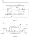
- FIGS. 1A, 1 B, 1 C and 1 D illustrated are top views and cross-sectional views of one advantageous embodiment of a completed transistor device 100 , manufactured according to the method described below.
- the views illustrated in FIGS. 1A and 1C will be described simultaneously, since they are identical.
- FIGS. 1A and 1C illustrates the completed transistor device 100 , including a source region 110 and a drain region 115 .
- the source region 110 and the drain region 115 have a source region contact 120 and a drain region contact 125 located therein.
- a transistor gate 130 having a gate sidewall spacer 135 connected thereto. Further illustrated in FIGS.
- FIGS. 1B and 1D are an oxide layer 140 , a nitrided layer 145 and an etch stop layer 150 .
- the oxide layer 140 , nitrided layer 145 and etch stop layer 150 are more easily understood with reference to the views illustrated in FIGS. 1B and 1D.
- FIG. 1B illustrated is a cross-sectional view taken through a line 1 B illustrated in FIG. 1 A.
- the cross-sectional view illustrates the source region 110 , the drain region 115 , the source contact region 120 , the drain contact region 125 , the transistor gate 130 and the gate sidewall spacer 135 .
- FIG. 1B which were also illustrated in FIGS. 1A and 1C, are the oxide layer 140 , nitrided layer 145 and the etch stop layer 150 .
- the semiconductor wafer substrate 165 may be any layer located in a semiconductor device, including a layer located at the wafer level or a layer located above wafer level. Also illustrated in FIG. 1B, but not in FIG. 1A, are a dielectric region 170 , a gate oxide 175 , a channel region 180 , and lightly doped source and drain regions 182 , 183 . As illustrated, the dielectric region 170 is located in a trench 185 in the semiconductor substrate 165 . As further illustrated, the source region 110 and drain region 115 are located in the trench 185 and at least partially on the dielectric region 170 . Likewise, as illustrated in FIG. 1B, the channel region 180 is located in the trench 185 between the source region 110 and the drain region 115 , and at least partially on the dielectric region 170 .
- FIG. 1D shown is a cross-sectional view taken through a line 1 D illustrated in FIG. 1 C.
- the cross-sectional view has many of the same features as the cross-sectional view illustrated in FIG. 1B, but taken through a different cross-section.
- the cross-section shown in FIG. 1D illustrates, the transistor gate 130 , the gate sidewall spacers 135 , the oxide layer 140 , the nitride layer 145 , the etch stop layer 150 , the semiconductor wafer-substrate 165 , the dielectric region 170 , the trench 185 and the channel region 180 .
- the completed transistor device 100 as illustrated in FIGS. 1A, 1 B, 1 C and 1 D reduces the parasitic capacitance and resistance associated with the prior art transistor devices. This is a result of the completed transistor device 100 being isolated from the substrate 165 and other possible capacitances by the dielectric region 170 .
- the dielectric region 170 in a preferred embodiment, is an oxide region having a dielectric constant three times higher than silicon, but much thicker than the equivalent dielectric in the source/drain region, resulting in a substantially lower capacitive coupling.
- the oxide layer 140 and nitride sidewall spacer 145 also help to reduce parasitic capacitance.
- the dielectric region 170 , the oxide layer 140 and the nitride sidewall spacers 145 not only reduce parasitic capacitance, but they substantially reduce “cross-talk” caused by transistors and other electrically noisy devices.
- the completed transistor device 100 also allows for improvement in the flexibility of the design of the completed device 100 through the use of innovative structures and processing steps. For example, in the case of FIGS. 1A-1D, it is clear that the punch through current of the transistor would be affected or limited by an electric field of the gate wrapping around the channel region on three sides, rather than one side, which is typical for the prior art devices.
- FIGS. 2A-15D illustrates a semiconductor wafer substrate 210 after formation of a thin etch stop layer 220 , using a conventional chemical vapor deposition (CVD) or other similar process.
- the etch stop layer 220 is formed over the entire surface of the semiconductor wafer substrate 210 .
- the etch stop layer 220 is a silicon nitride etch stop layer having a thickness of about 30 nm.
- the etch stop layer 220 may have a dual function, not only acting as an etch stop layer, but also preventing oxidation of the semiconductor wafer substrate 210 .
- the semiconductor wafer substrate 210 is a single crystal silicon semiconductor wafer substrate.
- FIG. 2B illustrated is the partially completed transistor device 200 illustrated in FIG. 2A, after formation of an oxide layer 225 over the etch stop layer 220 .
- the oxide layer 225 may be deposited using a conventional CVD, spin on glass (SOG) or other similar process, and in an exemplary embodiment is about 100 nm thick.
- the oxide layer 225 is a sacrificial layer that will be removed in a subsequent processing step.
- FIGS. 3A and 3B which represents a top view 302 and a cross-sectional view 305 , respectively, illustrated is the formation of a trench 310 within the partially completed transistor device 200 illustrated in FIG. 2 B. It is analogous to the device well in the field oxide for a transistor in the prior art.
- the trench 310 may be formed in many ways, but in an exemplary embodiment, a first dielectric trench etch is used to remove the desired oxide layer 225 and etch stop layer 220 , and a second silicon trench etch is used to produce a trench of the desired depth in the semiconductor wafer substrate 210 .
- the first dielectric trench etch is only used to remove the oxide layer 225
- the second silicon trench etch is used to remove the desired etch stop layer 220 and to produce a trench of the desired depth in the semiconductor wafer substrate 210 .
- the depth of the trench should be kept as shallow as possible to reduce the punch through current without impairing the ability of the metallization process to produce metal contacts with minimal contact resistance.
- the distance that the epitaxial growth must cover should be limited to facilitate that process. Therefore, a dimension of less than about 1000 nm is desirable.
- the stress relief pad oxide 410 may be formed using conventional pad oxide formation processes.
- the stress relief pad oxide 410 could be formed by a light oxidation process, oxide deposition process or other similar known process.
- the details of forming the stress relief pad oxide 410 are well known in the art, therefore, the process is not described in greater detail.
- the thickness of the stress relief pad oxide 410 in comparison to a thin layer of nitride described below, is a critical element.
- the thickness of the stress relief pad oxide 410 should be predetermined such that it reduces the vertical stress placed upon the semiconductor wafer substrate by a sidewall spacer and the dielectric region 610 (FIG. 6 ), formed in the following FIGURES.
- the stress relief pad oxide 410 has a thickness of about 15 nm.
- FIGS. 5A and 5B illustrated is the partially completed transistor device 200 illustrated in FIGS. 4A and 4B, after formation of sidewall spacers 510 .
- the sidewall spacers 510 are formed by depositing a thin layer of nitride over the surface of the partially completed transistor device 200 illustrated in FIGS. 4A and 4B, and performing a traditional anisotropic etch, resulting in the sidewall spacers 510 on the trench 310 walls.
- the dielectric region 610 such as an oxide region, is formed in the bottom of the trench 310 and within the semiconductor wafer substrate 210 .
- the dielectric region 610 has a thickness ranging from about 100 nm to about 200 nm, and more specifically a thickness of about 150 nm.
- the dielectric region 610 may be used, once the device is completed, to isolate the transistor device from the substrate 210 and also to reduce cross-talk between the transistor device and other semiconductor devices on the chip.
- FIG. 7 illustrated is the partially completed transistor device 200 illustrated in FIG. 6B, after a conformal deposition of a dielectric layer 710 over the oxide layer 225 and within the trench 310 .
- the dielectric layer 710 in an exemplary embodiment, is a sacrificial layer of spin on glass (SOG) or another similar material.
- the dielectric layer 710 as illustrated, may be formed over the entire semiconductor wafer substrate 210 .
- FIGS. 8A and 8B illustrated is the partially completed transistor device 200 illustrated in FIG. 7, after formation of an epitaxial channel 810 out of the dielectric layer 710 .
- One having skill in the art understands the conventional steps of depositing, patterning and developing photoresist, followed by a traditional etch, to define the epitaxial channel 810 .
- the epitaxial channel 810 should have a length of greater than about 1000 nm.
- the length of the epitaxial channel 810 may vary and is typically factored depending on the gate length, the sidewall spacer width, the contact dimension and the alignment and etch tolerances.
- FIGS. 9A and 9B illustrated is the partially completed transistor device 200 of FIGS. 8A and 8B, undergoing removal of the nitride sidewall spacer 510 and stress relief oxide 410 from one wall of the trench 310 .
- a conformal layer of photoresist is deposited, patterned and developed leaving a photoresist portion 910 , shown in FIGS. 9A and 9B.
- a conventional etch and removal of the sidewall spacer 510 and the stress relief oxide 410 from the trench 310 can then be conducted, resulting in the exposed wall of the trench 920 illustrated in FIGS. 9A and 9B.
- the exposed wall of the trench 920 may be subjected to a special sidewall clean to remove remaining residues. For instance, a wet oxidation of about 20 nm followed by an oxide strip, could be used to clean the exposed wall of the trench 920 . It should be noted that if the wet oxidation and wet oxidation oxide strip cleaning process were used, the thickness of the dielectric regions 610 should be sufficient to withstand both the stress relief pad oxide wet etch and the wet oxidation oxide strip.
- the photoresist portion 910 may be removed using conventional techniques.
- FIG. 10A and 10B illustrated is the formation of a source region 1010 , a channel region 1020 and a drain region 1030 .
- the partially completed transistor device 200 illustrated in FIGS. 9A and 9B may be placed within an ultra-clean environment and exposed to an n-type dopant gas, such as silane gas mixed with phosphine.
- the n-type dopant gas should react with the single crystal silicon present in the exposed wall of the trench 920 , and grow an epitaxial or single crystal layer outwards.
- the source region 1010 has a dopant concentration ranging from about 1E19/cm 3 to about 1E20/cm 3 .
- the channel region 1020 should be twice the gate width, and the source and drain regions 1010 , 1030 , should occupy the remaining space. However, the total width of all three regions 1010 , 1020 , 1030 , should be minimized for reasons of efficient packing, and to reduce the later epitaxial growth requirement.
- the partially completed transistor device 200 should remain within the ultra-clean environment while the gas is changed from an n-type dopant gas to a p-type dopant gas, such as diborane.
- the epitaxial silicon growth is further continued, resulting in the channel region 1020 illustrated in FIGS. 10B and 10B.
- the channel region 1020 is lightly doped, having a concentration ranging from about 1E16/cm 3 to about 1E17/cm 3 . Fortunately, the control of concentration profiling possible with epitaxy, is superior to many methods, thus, the final device would have relatively well controlled doping profiles.
- the partially completed transistor device 200 remains in the ultra-clean environment while the dopant gas is changed back to an n-type dopant gas, resulting in the drain region 1030 illustrated in FIGS. 10A and 10B.
- the drain region 1030 should have an n-type dopant concentration ranging from about 1E19/cm 3 to about 1E20/cm 3 , i.e., similar to the dopant concentration in the source region 1010 .
- the source region 1010 has a heavily doped source region 1004 and a lightly doped source region 1008 , the channel region 1020 remains lightly doped, and the drain region 1030 has a has a heavily doped drain region 1034 and a lightly doped drain region 1038 . Similar to the embodiment described in FIGS. 10A and 10B, the channel region 1020 is located between the source region 1010 and drain region 1030 . However, in the embodiment illustrated in FIGS. 10C and 10D, the channel region 1020 is located between the lightly doped source region 1008 and lightly doped drain region 1038 .
- the heavily doped source and drain regions 1004 , 1034 are doped with an n-type dopant to a concentration ranging from about 1E19/cm 3 to about 1E20/cm 3 and the lightly doped source and drain regions 1008 , 1038 , are doped with an n-type dopant to a concentration ranging from about 1E18/cm 3 to about 1E19/cm 3 .
- the channel region 1020 remains lightly doped with a p-type dopant to a concentration ranging from about 1E16/cm 3 to about 1E17/cm 3 .
- the present invention is not limited to the dopant concentrations mentioned above, and that the dopant concentration profile, taking into account dopant concentration and distance across the Epi channel, could be optimized to reduce punchthrough.
- the source and drain regions 1010 , 1030 could be interchanged by reversing the polarity of the voltages applied to the source and drain regions 1010 , 1030 , in the completed transistor device 100 , illustrated in FIGS. 1A, 1 B, 1 C and 1 D.
- NMOS n-type metal oxide semiconductor
- PMOS p-type metal oxide semiconductor
- FIGS. 11A and 11B illustrated is the partially completed transistor device 200 illustrated in FIGS. 10A and 10B, after a conventional chemical mechanical planarization (CMP) process.
- CMP chemical mechanical planarization
- the CMP process removes the excess dielectric layer 710 , the sacrificial oxide layer 225 and vertically over-grown epitaxial regions of the source region 1010 , channel region 1020 and drain region 1030 .
- the dielectric layer 710 remains in the trench 310 , but is removed from areas above the etch stop layer 220 .
- FIGS. 12A and 12B illustrated is the partially completed transistor device 200 illustrated in FIGS. 11A and 11B, after a subsequent dielectric layer 710 removal from the trench 310 .
- the dielectric layer 710 is removed from the trench 310 using a buffered hydrofluoric etch.
- a post 1210 comprising the source region 1010 , channel region 1020 and drain region 1030 .
- the post 1210 may be subjected to a wet pre-gate oxidation and a wet pre-gate oxidation etch.
- FIGS. 13A, 13 B, 13 C, and 13 D illustrated are various views of the partially completed transistor device 200 , illustrated in FIGS. 12A and 12B, after formation of a gate oxide layer 1310 .
- the gate oxide layer 1310 is formed to a thickness of about 10 nm or less.
- the gate oxide layer 1310 is formed over the source region 1010 , channel region 1020 and drain region 1030 .
- the gate oxide layer 1310 may be located on three sides of the source region 1010 , channel region 1020 and drain region 1030 .
- the three sides may refer to one horizontal surface and the two vertical surfaces, forming a channel region surrounded on three sides by a gate.
- the present invention is not limited to a gate oxide layer 1310 that is located on three sides of the source region 1010 , channel region 1020 and drain region 1030 , and that the gate oxide, in an alternative exemplary embodiment, could only be located on one side of the source region 1010 , channel region 1020 and drain region 1030 , as illustrated in FIGS. 16A-21D.
- FIGS. 14A, 14 B, 14 C and 14 D illustrated is the partially completed transistor device 200 illustrated in FIGS. 13A, 13 B, 13 C and 13 D, after formation of a transistor gate 1410 .
- a portion of the transistor gate 1410 is formed on the post and a portion is formed in the trench 310 .
- one having skill in the art knows how to form such a transistor gate 1410 , including: blanket depositing a gate poly material, doping the blanket deposited gate poly material, and patterning and etching the blanket deposited gate poly material, resulting in the transistor gate 1410 shown.
- the transistor gate 1410 is located over the gate oxide layer 1310 and over three sides of the channel region 1020 .
- FIGS. 15A, 15 B, 15 C and 15 D illustrated is the partially completed transistor device 200 illustrated in FIGS. 14A, 14 B, 14 C and 14 D after a lightly doped source 1510 and lightly doped drain 1520 region.
- the lightly doped drain and lightly doped source regions 1510 , 1520 may be located in the channel region 1020 , and in an exemplary embodiment are self-aligned to the transistor gate 1410 .
- One having skill in the art knows the standard methods used to form the lightly doped source and drain regions 1510 , 1520 .
- the lightly doped source and drain regions 1510 , 1520 should be doped with a similar dopant as the source and drain regions 1010 , 1030 .
- the lightly doped source and drain regions 1510 , 1520 should be doped with an n-type dopant, and vice-versa.
- the partially completed transistor device 200 may be subjected to a conformal deposition of a sidewall spacer layer.
- the sidewall spacer layer is an oxide sidewall spacer layer.
- the sidewall spacer layer may be etched, typically using a traditional anisotropic etch, resulting in gate sidewall spacers 1530 illustrated in FIGS. 15A, 15 B, 15 C and 15 D.
- the source and drain regions 1010 , 1030 may be subjected to a contact implant, resulting in a source contact implant 1540 and a drain contact implant 1550 .
- the source and drain contact implants 1540 , 1550 may be desired because, theoretically, they improve the contact resistance for vertical contacts, not shown.
- the partially completed transistor device 200 may be subjected to conventional contact and metallization processes, resulting in the completed transistor device 100 , illustrated in FIGS. 1A, 1 B, 1 C and 1 D.
- FIGS. 16A-21D illustrated are detailed manufacturing steps instructing how one might manufacture an alternative embodiment of the completed transistor device 100 depicted in FIGS. 1A, 1 B, 1 C and 1 D. Illustrated in FIGS. 16A and 16B, is an alternative embodiment partially completed transistor device 1600 , somewhat similar to the partially completed transistor device 200 , illustrated in FIGS. 10B and 10B. Moreover, the steps used to manufacture the alternative embodiment partially completed transistor device 1600 , illustrated in FIGS. 16A and 16B, are similar to the manufacturing steps depicted in FIGS. 2A-9B. One of the only differences between the alternative embodiment partially completed transistor device 1600 and the partially completed transistor device 200 , illustrated in FIGS.
- the epitaxial silicon, grown from the exposed wall of the trench 920 does not include the heavily doped source and drain regions 1010 , 1030 (FIG. 10 ).
- the alternative embodiment partially completed transistor device 1600 depicted in FIGS. 16A and 16B contains one lightly doped channel region 1610 .
- the lightly doped channel region 1610 is doped with a p-type dopant to a concentration ranging from about 1E16/cm 3 to about 1E17/cm 3 .
- FIGS. 17A and 17B illustrated is the alternative embodiment partially completed transistor device 1600 , illustrated in FIGS. 16A and 16B, after a conventional chemical mechanical planarization (CMP) process.
- CMP chemical mechanical planarization
- the CMP process removes the excess dielectric layer 710 , the sacrificial oxide layer 225 and vertically over-grown epitaxial regions of the channel region 1610 .
- the dielectric layer 710 remains in the trench 310 , but is removed from areas above the etch stop layer 220 .
- the present embodiment has the dielectric layer 710 remaining in the trench 310 .
- FIGS. 18A, 18 B, 18 C, and 18 D illustrated are various views of the alternative embodiment partially completed transistor device 1600 , illustrated in FIGS. 17A and 17B, after formation of a gate oxide layer 1810 .
- the gate oxide layer 1810 is formed to a thickness of about 10 nm or less.
- the gate oxide layer 1310 is formed over the channel region 1610 .
- the gate oxide layer 1810 is only located on one side (the top surface) of the channel region 1610 .
- the channel region 1610 may be subjected to a wet pre-gate oxidation and a wet pre-gate oxidation etch, prior to formation of the gate oxide layer 1810 .
- a threshold adjustment implant could, in an exemplary embodiment, be conducted prior to formation of the gate oxide layer 1810 .
- FIGS. 19A, 19 B, 19 C and 19 D illustrated is the alternative embodiment partially completed transistor device 1600 illustrated in FIGS. 18A, 18 B, 18 C and 18 D, after formation of a transistor gate 1910 .
- the transistor gate 1910 is formed at least partially over the dielectric layer 710 .
- the transistor gate 1910 includes: blanket depositing a gate poly material, doping the blanket deposited gate poly material, and patterning and etching the blanket deposited gate poly material, resulting in the transistor gate 1910 shown.
- the transistor gate 1910 is located over the gate oxide layer 1810 and channel region 1610 .
- FIGS. 20A, 20 B, 20 C and 20 D illustrated is the partially completed transistor device 1600 illustrated in FIGS. 19A, 19 B, 19 C and 19 D after a lightly doped source 2010 and lightly doped drain 2020 implant.
- the light doped source and lightly doped drain implants 2010 , 2020 are located in the channel region 1610 , and in an exemplary embodiment are self-aligned to the transistor gate 1910 .
- One having skill in the art knows the standard methods used to form lightly doped source and drain regions 2010 , 2020 .
- the lightly doped source and drain regions 2010 , 2020 should be doped with an opposite dopant as used when forming the channel region 1610 .
- the lightly doped source and drain regions 2010 , 2020 should be doped with an n-type dopant, and vice-versa.
- the alternative embodiment partially completed transistor device 1600 may be subjected to a conformal deposition of a sidewall spacer layer.
- the sidewall spacer layer is an oxide sidewall spacer layer.
- the sidewall spacer layer may be etched, typically using a traditional anisotropic etch, resulting in gate sidewall spacers 2030 illustrated in FIGS. 20A, 20 B, 20 C and 20 D.
- FIGS. 21A, 21 B, 21 C and 21 D illustrated is the formation of a heavily doped source region 2110 and a heavily doped drain region 2120 .
- One having skill in the art knows how to form the heavily doped source and drain regions 2110 , 2120 , including patterning a layer of photoresist to leave unprotected portions where the heavily doped source and drain regions 2110 , 2120 , are desired, and doping the unprotected portions with an n-type dopant.
- it is desired for the heavily doped source and drain regions 2110 , 2120 to have a concentration of the n-type dopant ranging from about 1E19/cm 3 to about 1E20/cm 3 .
- the alternative embodiment partially completed transistor device 1600 could be subjected to conventional contact and metallization processes, resulting in a completed alternative embodiment transistor device.
- the integrated circuit 2500 may include the completed transistor device 100 , illustrated in FIGS. 1A, 1 B, 1 C and 1 D, including: the source region 110 , drain region 115 , source region contact 120 , drain region contact 125 , transistor gate 130 , and dielectric region 170 .
- the transistor device 100 may for part of a complementary metal oxide semiconductor (CMOS) device, bipolar CMOS (BiCMOS) device or any other type of similar device.
- CMOS complementary metal oxide semiconductor
- BiCMOS bipolar CMOS
- dielectric layers 2210 are shown in one advantageous embodiment of the integrated circuit 2200 .
- interconnect structures 2220 may be located within the dielectric layer 2210 , to contact the source region 110 , drain region 115 and transistor gate 130 , to form the operational integrated circuit 2200 .
Abstract
Description
Claims (27)
Priority Applications (1)
| Application Number | Priority Date | Filing Date | Title |
|---|---|---|---|
| US09/653,531 US6630699B1 (en) | 2000-08-31 | 2000-08-31 | Transistor device having an isolation structure located under a source region, drain region and channel region and a method of manufacture thereof |
Applications Claiming Priority (1)
| Application Number | Priority Date | Filing Date | Title |
|---|---|---|---|
| US09/653,531 US6630699B1 (en) | 2000-08-31 | 2000-08-31 | Transistor device having an isolation structure located under a source region, drain region and channel region and a method of manufacture thereof |
Publications (1)
| Publication Number | Publication Date |
|---|---|
| US6630699B1 true US6630699B1 (en) | 2003-10-07 |
Family
ID=28675750
Family Applications (1)
| Application Number | Title | Priority Date | Filing Date |
|---|---|---|---|
| US09/653,531 Expired - Lifetime US6630699B1 (en) | 2000-08-31 | 2000-08-31 | Transistor device having an isolation structure located under a source region, drain region and channel region and a method of manufacture thereof |
Country Status (1)
| Country | Link |
|---|---|
| US (1) | US6630699B1 (en) |
Cited By (12)
| Publication number | Priority date | Publication date | Assignee | Title |
|---|---|---|---|---|
| US20040033666A1 (en) * | 2002-08-14 | 2004-02-19 | Williams Richard K. | Isolated complementary MOS devices in epi-less substrate |
| US20040063291A1 (en) * | 2002-09-29 | 2004-04-01 | Williams Richard K. | Modular bipolar-CMOS-DMOS analog integrated circuit & power transistor technology |
| US20050164454A1 (en) * | 2004-01-27 | 2005-07-28 | Micron Technology, Inc. | Selective epitaxy vertical integrated circuit components and methods |
| US20050227498A1 (en) * | 2004-03-31 | 2005-10-13 | International Business Machines Corporation | Method for fabricating strained silicon-on-insulator structures and strained silicon-on insulator structures formed thereby |
| US20060033179A1 (en) * | 2004-08-16 | 2006-02-16 | Chao-Tzung Tsai | Retrograde trench isolation structures |
| US20080167196A1 (en) * | 2000-02-06 | 2008-07-10 | Stefan Dickopf | Surface for the immobilization of ligands |
| US20090045482A1 (en) * | 2007-08-14 | 2009-02-19 | Jhon-Jhy Liaw | Shallow Trench Isolation with Improved Structure and Method of Forming |
| US7863133B2 (en) | 2005-06-28 | 2011-01-04 | Micron Technology, Inc. | Oxide epitaxial isolation |
| US20110298010A1 (en) * | 2010-02-09 | 2011-12-08 | Stmicroelectronics Sa | Cell Library, Integrated Circuit, and Methods of Making Same |
| US9087853B2 (en) * | 2013-10-25 | 2015-07-21 | Avago Technologies General Ip (Singapore) Pte. Ltd. | Isolation device |
| US9257504B2 (en) | 2002-09-29 | 2016-02-09 | Advanced Analogic Technologies Incorporated | Isolation structures for semiconductor devices |
| US11069680B2 (en) | 2019-03-28 | 2021-07-20 | International Business Machines Corporation | FinFET-based integrated circuits with reduced parasitic capacitance |
Citations (2)
| Publication number | Priority date | Publication date | Assignee | Title |
|---|---|---|---|---|
| US5428243A (en) | 1993-01-07 | 1995-06-27 | Northern Telecom Limited | Bipolar transistor with a self-aligned heavily doped collector region and base link regions. |
| US20010016383A1 (en) * | 1999-06-04 | 2001-08-23 | Chen Howard H. | Method for fabricating complementary metal oxide semiconductor (CMOS) devices on a mixed bulk and silicon-on-insulator (SOI) substrate |
-
2000
- 2000-08-31 US US09/653,531 patent/US6630699B1/en not_active Expired - Lifetime
Patent Citations (2)
| Publication number | Priority date | Publication date | Assignee | Title |
|---|---|---|---|---|
| US5428243A (en) | 1993-01-07 | 1995-06-27 | Northern Telecom Limited | Bipolar transistor with a self-aligned heavily doped collector region and base link regions. |
| US20010016383A1 (en) * | 1999-06-04 | 2001-08-23 | Chen Howard H. | Method for fabricating complementary metal oxide semiconductor (CMOS) devices on a mixed bulk and silicon-on-insulator (SOI) substrate |
Cited By (64)
| Publication number | Priority date | Publication date | Assignee | Title |
|---|---|---|---|---|
| US20080167196A1 (en) * | 2000-02-06 | 2008-07-10 | Stefan Dickopf | Surface for the immobilization of ligands |
| US20050142792A1 (en) * | 2002-08-14 | 2005-06-30 | Advanced Analogic Technologies, Inc. | Method of fabricating isolated semiconductor devices in epi-less substrate |
| US7449380B2 (en) | 2002-08-14 | 2008-11-11 | Advanced Analogic Technologies, Inc. | Method of fabricating isolated semiconductor devices in epi-less substrate |
| US20050142791A1 (en) * | 2002-08-14 | 2005-06-30 | Advanced Analogic Technologies, Inc. | Method of fabricating isolated semiconductor devices in epi-less substrate |
| US20050014324A1 (en) * | 2002-08-14 | 2005-01-20 | Advanced Analogic Technologies, Inc. | Method of fabricating isolated semiconductor devices in epi-less substrate |
| US20050158939A1 (en) * | 2002-08-14 | 2005-07-21 | Advanced Analogic Technologies, Inc | Method of fabricating isolated semiconductor devices in epi-less substrate |
| US6900091B2 (en) | 2002-08-14 | 2005-05-31 | Advanced Analogic Technologies, Inc. | Isolated complementary MOS devices in epi-less substrate |
| US20050142724A1 (en) * | 2002-08-14 | 2005-06-30 | Advanced Analogic Technologies, Inc. | Method of fabricating isolated semiconductor devices in epi-less substrate |
| US7445979B2 (en) | 2002-08-14 | 2008-11-04 | Advanced Analogic Technologies, Inc. | Method of fabricating isolated semiconductor devices in epi-less substrate |
| US20050014329A1 (en) * | 2002-08-14 | 2005-01-20 | Advanced Analogic Technologies, Inc. | Method of fabricating isolated semiconductor devices in epi-less substrate |
| US7666756B2 (en) | 2002-08-14 | 2010-02-23 | Advanced Analogic Technologies, Inc. | Methods of fabricating isolation structures in epi-less substrate |
| US7276431B2 (en) | 2002-08-14 | 2007-10-02 | Advanced Analogic Technologies, Inc. | Method of fabricating isolated semiconductor devices in epi-less substrate |
| US7422938B2 (en) | 2002-08-14 | 2008-09-09 | Advanced Analogic Technologies, Inc. | Method of fabricating isolated semiconductor devices in epi-less substrate |
| WO2004017395A1 (en) * | 2002-08-14 | 2004-02-26 | Advanced Analogic Technologies, Inc. | Isolated complementary mos devices in epi-less substrate |
| US20040033666A1 (en) * | 2002-08-14 | 2004-02-19 | Williams Richard K. | Isolated complementary MOS devices in epi-less substrate |
| US7329583B2 (en) | 2002-08-14 | 2008-02-12 | Advanced Analogic Technologies, Inc. | Method of fabricating isolated semiconductor devices in epi-less substrate |
| US20060223257A1 (en) * | 2002-08-14 | 2006-10-05 | Advanced Analogic Technologies, Inc. | Method Of Fabricating Isolated Semiconductor Devices In Epi-Less Substrate |
| US7279378B2 (en) | 2002-08-14 | 2007-10-09 | Advanced Analogic Technologies, Inc. | Method of fabricating isolated semiconductor devices in epi-less substrate |
| US20080116513A1 (en) * | 2002-09-29 | 2008-05-22 | Advanced Analogic Technologies, Inc. | Modular bipolar-CMOS-DMOS analog integrated circuit and power transistor technology |
| US7573105B2 (en) | 2002-09-29 | 2009-08-11 | Advanced Analogic Technologies, Inc. | Modular bipolar-CMOS-DMOS analog integrated circuit and power transistor technology |
| US7265434B2 (en) | 2002-09-29 | 2007-09-04 | Advanced Analogic Technologies, Inc. | Modular bipolar-CMOS-DMOS analog integrated circuit and power transistor technology |
| US7202536B2 (en) | 2002-09-29 | 2007-04-10 | Advanced Analogic Technologies, Inc. | Modular bipolar-CMOS-DMOS analog integrated circuit and power transistor technology |
| US7135738B2 (en) * | 2002-09-29 | 2006-11-14 | Advanced Analogic Technologies, Inc. | Modular bipolar-CMOS-DMOS analog integrated circuit and power transistor technology |
| US7279399B2 (en) * | 2002-09-29 | 2007-10-09 | Advanced Analogic Technologies, Inc. | Method of forming isolated pocket in a semiconductor substrate |
| US20070272986A1 (en) * | 2002-09-29 | 2007-11-29 | Advanced Analogic Technologies, Inc. | Modular bipolar-CMOS-DMOS analog integrated circuit and power transistor technology |
| US20080023762A1 (en) * | 2002-09-29 | 2008-01-31 | Advanced Analogic Technologies, Inc. | Modular bipolar-CMOS-DMOS analog integrated circuit and power transistor technology |
| US20060157818A1 (en) * | 2002-09-29 | 2006-07-20 | Advanced Analogic Technologies, Inc. | Modular bipolar-CMOS-DMOS analog integrated circuit and power transistor technology |
| US10074716B2 (en) | 2002-09-29 | 2018-09-11 | Skyworks Solutions (Hong Kong) Limited | Saucer-shaped isolation structures for semiconductor devices |
| US9905640B2 (en) | 2002-09-29 | 2018-02-27 | Skyworks Solutions (Hong Kong) Limited | Isolation structures for semiconductor devices including trenches containing conductive material |
| US20080061375A1 (en) * | 2002-09-29 | 2008-03-13 | Advanced Analogic Technologies, Inc. | Modular bipolar-CMOS-DMOS analog integrated circuit and power transistor technology |
| US20080061377A1 (en) * | 2002-09-29 | 2008-03-13 | Advanced Analogic Technologies, Inc. | Modular bipolar-CMOS-DMOS analog integrated circuit and power transistor technology |
| US20080061376A1 (en) * | 2002-09-29 | 2008-03-13 | Advanced Analogic Technologies, Inc. | Modular bipolar-CMOS-DMOS analog integrated circuit & power transistor technology |
| US9257504B2 (en) | 2002-09-29 | 2016-02-09 | Advanced Analogic Technologies Incorporated | Isolation structures for semiconductor devices |
| US7745883B2 (en) | 2002-09-29 | 2010-06-29 | Advanced Analogic Technologies, Inc. | Modular bipolar-CMOS-DMOS analog integrated circuit and power transistor technology |
| US20040063291A1 (en) * | 2002-09-29 | 2004-04-01 | Williams Richard K. | Modular bipolar-CMOS-DMOS analog integrated circuit & power transistor technology |
| US7608895B2 (en) | 2002-09-29 | 2009-10-27 | Advanced Analogic Technologies, Inc. | Modular CMOS analog integrated circuit and power technology |
| US7605432B2 (en) | 2002-09-29 | 2009-10-20 | Advanced Analogic Technologies, Inc. | Modular bipolar-CMOS-DMOS analog integrated circuit and power transistor technology |
| US6855985B2 (en) * | 2002-09-29 | 2005-02-15 | Advanced Analogic Technologies, Inc. | Modular bipolar-CMOS-DMOS analog integrated circuit & power transistor technology |
| US7605433B2 (en) | 2002-09-29 | 2009-10-20 | Advanced Analogic Technologies, Inc. | Modular bipolar-CMOS-DMOS analog integrated circuit and power transistor technology |
| US7602024B2 (en) | 2002-09-29 | 2009-10-13 | Advanced Analogic Technologies, Inc. | Modular bipolar-CMOS-DMOS analog integrated circuit and power transistor technology |
| US7602023B2 (en) | 2002-09-29 | 2009-10-13 | Advanced Analogic Technologies, Inc. | Modular bipolar-CMOS-DMOS analog integrated circuit and power transistor technology |
| US7211863B2 (en) * | 2002-09-29 | 2007-05-01 | Advanced Analogic Technologies, Inc. | Modular bipolar-CMOS-DMOS analog integrated circuit and power transistor technology |
| US7851309B2 (en) | 2004-01-27 | 2010-12-14 | Micron Technology, Inc. | Selective epitaxy vertical integrated circuit components and methods |
| US7514324B2 (en) | 2004-01-27 | 2009-04-07 | Micron Technology, Inc. | Selective epitaxy in vertical integrated circuit |
| US20090197379A1 (en) * | 2004-01-27 | 2009-08-06 | Leslie Terrence C | Selective epitaxy vertical integrated circuit components and methods |
| US20050164454A1 (en) * | 2004-01-27 | 2005-07-28 | Micron Technology, Inc. | Selective epitaxy vertical integrated circuit components and methods |
| US7372091B2 (en) | 2004-01-27 | 2008-05-13 | Micron Technology, Inc. | Selective epitaxy vertical integrated circuit components |
| US20060006444A1 (en) * | 2004-01-27 | 2006-01-12 | Micron Technology, Inc. | Selective epitaxy vertical integrated circuit components and methods |
| US20050227498A1 (en) * | 2004-03-31 | 2005-10-13 | International Business Machines Corporation | Method for fabricating strained silicon-on-insulator structures and strained silicon-on insulator structures formed thereby |
| US7704855B2 (en) | 2004-03-31 | 2010-04-27 | International Business Machines Corporation | Method for fabricating strained silicon-on-insulator structures and strained silicon-on-insulator structures formed thereby |
| CN1914722B (en) * | 2004-03-31 | 2013-01-23 | 国际商业机器公司 | Method for fabricating strained silicon-on-insulator structures and strained silicon-on-insulator structures formed thereby |
| US8450806B2 (en) * | 2004-03-31 | 2013-05-28 | International Business Machines Corporation | Method for fabricating strained silicon-on-insulator structures and strained silicon-on insulator structures formed thereby |
| US20080050931A1 (en) * | 2004-03-31 | 2008-02-28 | International Business Machines Corporation | Method for fabricating strained silicon-on-insulator structures and strained silicon-on-insulator structures formed thereby |
| US20060033179A1 (en) * | 2004-08-16 | 2006-02-16 | Chao-Tzung Tsai | Retrograde trench isolation structures |
| US7339253B2 (en) | 2004-08-16 | 2008-03-04 | Taiwan Semiconductor Manufacturing Company | Retrograde trench isolation structures |
| US7863133B2 (en) | 2005-06-28 | 2011-01-04 | Micron Technology, Inc. | Oxide epitaxial isolation |
| US20090045482A1 (en) * | 2007-08-14 | 2009-02-19 | Jhon-Jhy Liaw | Shallow Trench Isolation with Improved Structure and Method of Forming |
| US8120094B2 (en) | 2007-08-14 | 2012-02-21 | Taiwan Semiconductor Manufacturing Co., Ltd. | Shallow trench isolation with improved structure and method of forming |
| US8409964B2 (en) | 2007-08-14 | 2013-04-02 | Taiwan Semiconductor Manufacturing Company, Ltd. | Shallow trench isolation with improved structure and method of forming |
| US20110298010A1 (en) * | 2010-02-09 | 2011-12-08 | Stmicroelectronics Sa | Cell Library, Integrated Circuit, and Methods of Making Same |
| US8458638B2 (en) * | 2010-02-09 | 2013-06-04 | Stmicroelectronics Sa | Cell library, integrated circuit, and methods of making same |
| US9087853B2 (en) * | 2013-10-25 | 2015-07-21 | Avago Technologies General Ip (Singapore) Pte. Ltd. | Isolation device |
| US10211281B2 (en) | 2013-10-25 | 2019-02-19 | Avago Technologies International Sales Pte. Limited | Isolation device |
| US11069680B2 (en) | 2019-03-28 | 2021-07-20 | International Business Machines Corporation | FinFET-based integrated circuits with reduced parasitic capacitance |
Similar Documents
| Publication | Publication Date | Title |
|---|---|---|
| KR100687130B1 (en) | Device threshold control of front-gate silicon-on-insulator mosfet using a self-aligned back-gate | |
| KR100366965B1 (en) | Soi cmos body contact through gate, self-aligned to source-drain diffusions | |
| US8367490B2 (en) | Semiconductor structure and method for manufacturing the same | |
| US6084271A (en) | Transistor with local insulator structure | |
| US6225173B1 (en) | Recessed channel structure for manufacturing shallow source/drain extensions | |
| US6392271B1 (en) | Structure and process flow for fabrication of dual gate floating body integrated MOS transistors | |
| US8502316B2 (en) | Self-aligned two-step STI formation through dummy poly removal | |
| US7105399B1 (en) | Selective epitaxial growth for tunable channel thickness | |
| US7141476B2 (en) | Method of forming a transistor with a bottom gate | |
| US20030222313A1 (en) | Self-aligned body tie for a partially depleted SOI device structure | |
| US6864547B2 (en) | Semiconductor device having a ghost source/drain region and a method of manufacture therefor | |
| US6506638B1 (en) | Vertical double gate transistor structure | |
| JP2002343883A (en) | Cmos structure with non-epitaxial raised source/drain and self-aligned gate, and method of manufacturing the same | |
| US6630699B1 (en) | Transistor device having an isolation structure located under a source region, drain region and channel region and a method of manufacture thereof | |
| US6548362B1 (en) | Method of forming MOSFET with buried contact and air-gap gate structure | |
| WO2014162164A1 (en) | Cmos in situ doped flow with independently tunable spacer thickness | |
| US9178070B2 (en) | Semiconductor structure and method for manufacturing the same | |
| US20020090787A1 (en) | Self-aligned elevated transistor | |
| US6509218B2 (en) | Front stage process of a fully depleted silicon-on-insulator device | |
| US6958518B2 (en) | Semiconductor device having at least one source/drain region formed on an isolation region and a method of manufacture therefor | |
| US6127212A (en) | Method of forming a CMOS transistor | |
| US7198993B2 (en) | Method of fabricating a combined fully-depleted silicon-on-insulator (FD-SOI) and partially-depleted silicon-on-insulator (PD-SOI) devices | |
| US6380038B1 (en) | Transistor with electrically induced source/drain extensions | |
| US6853048B1 (en) | Bipolar transistor having an isolation structure located under the base, emitter and collector and a method of manufacture thereof | |
| KR20040009748A (en) | Method of Fabricating MOS Transistor |
Legal Events
| Date | Code | Title | Description |
|---|---|---|---|
| AS | Assignment |
Owner name: LUCENT TECHNOLOGIES, INC., NEW JERSEY Free format text: ASSIGNMENT OF ASSIGNORS INTEREST;ASSIGNOR:WYLIE, IAN;REEL/FRAME:011297/0499 Effective date: 20000920 |
|
| STCF | Information on status: patent grant |
Free format text: PATENTED CASE |
|
| AS | Assignment |
Owner name: AGERE SYSTEMS INC., PENNSYLVANIA Free format text: ASSIGNMENT OF ASSIGNORS INTEREST;ASSIGNOR:LUCENT TECHNOLOGIES INC.;REEL/FRAME:014981/0676 Effective date: 20010730 |
|
| FPAY | Fee payment |
Year of fee payment: 4 |
|
| FPAY | Fee payment |
Year of fee payment: 8 |
|
| AS | Assignment |
Owner name: DEUTSCHE BANK AG NEW YORK BRANCH, AS COLLATERAL AG Free format text: PATENT SECURITY AGREEMENT;ASSIGNORS:LSI CORPORATION;AGERE SYSTEMS LLC;REEL/FRAME:032856/0031 Effective date: 20140506 |
|
| FPAY | Fee payment |
Year of fee payment: 12 |
|
| AS | Assignment |
Owner name: AVAGO TECHNOLOGIES GENERAL IP (SINGAPORE) PTE. LTD Free format text: ASSIGNMENT OF ASSIGNORS INTEREST;ASSIGNOR:AGERE SYSTEMS LLC;REEL/FRAME:035365/0634 Effective date: 20140804 |
|
| AS | Assignment |
Owner name: LSI CORPORATION, CALIFORNIA Free format text: TERMINATION AND RELEASE OF SECURITY INTEREST IN PATENT RIGHTS (RELEASES RF 032856-0031);ASSIGNOR:DEUTSCHE BANK AG NEW YORK BRANCH, AS COLLATERAL AGENT;REEL/FRAME:037684/0039 Effective date: 20160201 Owner name: AGERE SYSTEMS LLC, PENNSYLVANIA Free format text: TERMINATION AND RELEASE OF SECURITY INTEREST IN PATENT RIGHTS (RELEASES RF 032856-0031);ASSIGNOR:DEUTSCHE BANK AG NEW YORK BRANCH, AS COLLATERAL AGENT;REEL/FRAME:037684/0039 Effective date: 20160201 |
|
| AS | Assignment |
Owner name: BANK OF AMERICA, N.A., AS COLLATERAL AGENT, NORTH CAROLINA Free format text: PATENT SECURITY AGREEMENT;ASSIGNOR:AVAGO TECHNOLOGIES GENERAL IP (SINGAPORE) PTE. LTD.;REEL/FRAME:037808/0001 Effective date: 20160201 Owner name: BANK OF AMERICA, N.A., AS COLLATERAL AGENT, NORTH Free format text: PATENT SECURITY AGREEMENT;ASSIGNOR:AVAGO TECHNOLOGIES GENERAL IP (SINGAPORE) PTE. LTD.;REEL/FRAME:037808/0001 Effective date: 20160201 |
|
| AS | Assignment |
Owner name: AVAGO TECHNOLOGIES GENERAL IP (SINGAPORE) PTE. LTD., SINGAPORE Free format text: TERMINATION AND RELEASE OF SECURITY INTEREST IN PATENTS;ASSIGNOR:BANK OF AMERICA, N.A., AS COLLATERAL AGENT;REEL/FRAME:041710/0001 Effective date: 20170119 Owner name: AVAGO TECHNOLOGIES GENERAL IP (SINGAPORE) PTE. LTD Free format text: TERMINATION AND RELEASE OF SECURITY INTEREST IN PATENTS;ASSIGNOR:BANK OF AMERICA, N.A., AS COLLATERAL AGENT;REEL/FRAME:041710/0001 Effective date: 20170119 |
|
| AS | Assignment |
Owner name: BELL SEMICONDUCTOR, LLC, ILLINOIS Free format text: ASSIGNMENT OF ASSIGNORS INTEREST;ASSIGNORS:AVAGO TECHNOLOGIES GENERAL IP (SINGAPORE) PTE. LTD.;BROADCOM CORPORATION;REEL/FRAME:044886/0001 Effective date: 20171208 |
|
| AS | Assignment |
Owner name: CORTLAND CAPITAL MARKET SERVICES LLC, AS COLLATERA Free format text: SECURITY INTEREST;ASSIGNORS:HILCO PATENT ACQUISITION 56, LLC;BELL SEMICONDUCTOR, LLC;BELL NORTHERN RESEARCH, LLC;REEL/FRAME:045216/0020 Effective date: 20180124 |
|
| AS | Assignment |
Owner name: BELL NORTHERN RESEARCH, LLC, ILLINOIS Free format text: SECURITY INTEREST;ASSIGNOR:CORTLAND CAPITAL MARKET SERVICES LLC;REEL/FRAME:060885/0001 Effective date: 20220401 Owner name: BELL SEMICONDUCTOR, LLC, ILLINOIS Free format text: SECURITY INTEREST;ASSIGNOR:CORTLAND CAPITAL MARKET SERVICES LLC;REEL/FRAME:060885/0001 Effective date: 20220401 Owner name: HILCO PATENT ACQUISITION 56, LLC, ILLINOIS Free format text: SECURITY INTEREST;ASSIGNOR:CORTLAND CAPITAL MARKET SERVICES LLC;REEL/FRAME:060885/0001 Effective date: 20220401 |