US6630628B2 - High-performance laminate for integrated circuit interconnection - Google Patents
High-performance laminate for integrated circuit interconnection Download PDFInfo
- Publication number
- US6630628B2 US6630628B2 US10/072,261 US7226102A US6630628B2 US 6630628 B2 US6630628 B2 US 6630628B2 US 7226102 A US7226102 A US 7226102A US 6630628 B2 US6630628 B2 US 6630628B2
- Authority
- US
- United States
- Prior art keywords
- layer
- laminate
- open areas
- recited
- printed circuit
- Prior art date
- Legal status (The legal status is an assumption and is not a legal conclusion. Google has not performed a legal analysis and makes no representation as to the accuracy of the status listed.)
- Expired - Fee Related
Links
Images


Classifications
-
- H—ELECTRICITY
- H05—ELECTRIC TECHNIQUES NOT OTHERWISE PROVIDED FOR
- H05K—PRINTED CIRCUITS; CASINGS OR CONSTRUCTIONAL DETAILS OF ELECTRIC APPARATUS; MANUFACTURE OF ASSEMBLAGES OF ELECTRICAL COMPONENTS
- H05K1/00—Printed circuits
- H05K1/02—Details
- H05K1/0213—Electrical arrangements not otherwise provided for
- H05K1/0216—Reduction of cross-talk, noise or electromagnetic interference
- H05K1/0218—Reduction of cross-talk, noise or electromagnetic interference by printed shielding conductors, ground planes or power plane
- H05K1/0224—Patterned shielding planes, ground planes or power planes
-
- H—ELECTRICITY
- H10—SEMICONDUCTOR DEVICES; ELECTRIC SOLID-STATE DEVICES NOT OTHERWISE PROVIDED FOR
- H10W—GENERIC PACKAGES, INTERCONNECTIONS, CONNECTORS OR OTHER CONSTRUCTIONAL DETAILS OF DEVICES COVERED BY CLASS H10
- H10W70/00—Package substrates; Interposers; Redistribution layers [RDL]
- H10W70/60—Insulating or insulated package substrates; Interposers; Redistribution layers
- H10W70/62—Insulating or insulated package substrates; Interposers; Redistribution layers characterised by their interconnections
- H10W70/65—Shapes or dispositions of interconnections
-
- H—ELECTRICITY
- H10—SEMICONDUCTOR DEVICES; ELECTRIC SOLID-STATE DEVICES NOT OTHERWISE PROVIDED FOR
- H10W—GENERIC PACKAGES, INTERCONNECTIONS, CONNECTORS OR OTHER CONSTRUCTIONAL DETAILS OF DEVICES COVERED BY CLASS H10
- H10W70/00—Package substrates; Interposers; Redistribution layers [RDL]
- H10W70/60—Insulating or insulated package substrates; Interposers; Redistribution layers
- H10W70/67—Insulating or insulated package substrates; Interposers; Redistribution layers characterised by their insulating layers or insulating parts
- H10W70/68—Shapes or dispositions thereof
- H10W70/685—Shapes or dispositions thereof comprising multiple insulating layers
-
- H—ELECTRICITY
- H05—ELECTRIC TECHNIQUES NOT OTHERWISE PROVIDED FOR
- H05K—PRINTED CIRCUITS; CASINGS OR CONSTRUCTIONAL DETAILS OF ELECTRIC APPARATUS; MANUFACTURE OF ASSEMBLAGES OF ELECTRICAL COMPONENTS
- H05K1/00—Printed circuits
- H05K1/02—Details
- H05K1/0213—Electrical arrangements not otherwise provided for
- H05K1/0237—High frequency adaptations
- H05K1/025—Impedance arrangements, e.g. impedance matching, reduction of parasitic impedance
- H05K1/0253—Impedance adaptations of transmission lines by special lay-out of power planes, e.g. providing openings
-
- H—ELECTRICITY
- H05—ELECTRIC TECHNIQUES NOT OTHERWISE PROVIDED FOR
- H05K—PRINTED CIRCUITS; CASINGS OR CONSTRUCTIONAL DETAILS OF ELECTRIC APPARATUS; MANUFACTURE OF ASSEMBLAGES OF ELECTRICAL COMPONENTS
- H05K2201/00—Indexing scheme relating to printed circuits covered by H05K1/00
- H05K2201/09—Shape and layout
- H05K2201/09209—Shape and layout details of conductors
- H05K2201/09218—Conductive traces
- H05K2201/09227—Layout details of a plurality of traces, e.g. escape layout for Ball Grid Array [BGA] mounting
-
- H—ELECTRICITY
- H05—ELECTRIC TECHNIQUES NOT OTHERWISE PROVIDED FOR
- H05K—PRINTED CIRCUITS; CASINGS OR CONSTRUCTIONAL DETAILS OF ELECTRIC APPARATUS; MANUFACTURE OF ASSEMBLAGES OF ELECTRICAL COMPONENTS
- H05K2201/00—Indexing scheme relating to printed circuits covered by H05K1/00
- H05K2201/09—Shape and layout
- H05K2201/09209—Shape and layout details of conductors
- H05K2201/09654—Shape and layout details of conductors covering at least two types of conductors provided for in H05K2201/09218 - H05K2201/095
- H05K2201/09672—Superposed layout, i.e. in different planes
-
- H—ELECTRICITY
- H05—ELECTRIC TECHNIQUES NOT OTHERWISE PROVIDED FOR
- H05K—PRINTED CIRCUITS; CASINGS OR CONSTRUCTIONAL DETAILS OF ELECTRIC APPARATUS; MANUFACTURE OF ASSEMBLAGES OF ELECTRICAL COMPONENTS
- H05K2201/00—Indexing scheme relating to printed circuits covered by H05K1/00
- H05K2201/09—Shape and layout
- H05K2201/09209—Shape and layout details of conductors
- H05K2201/09654—Shape and layout details of conductors covering at least two types of conductors provided for in H05K2201/09218 - H05K2201/095
- H05K2201/09681—Mesh conductors, e.g. as a ground plane
-
- H—ELECTRICITY
- H05—ELECTRIC TECHNIQUES NOT OTHERWISE PROVIDED FOR
- H05K—PRINTED CIRCUITS; CASINGS OR CONSTRUCTIONAL DETAILS OF ELECTRIC APPARATUS; MANUFACTURE OF ASSEMBLAGES OF ELECTRICAL COMPONENTS
- H05K2203/00—Indexing scheme relating to apparatus or processes for manufacturing printed circuits covered by H05K3/00
- H05K2203/11—Treatments characterised by their effect, e.g. heating, cooling, roughening
- H05K2203/1178—Means for venting or for letting gases escape
-
- H—ELECTRICITY
- H05—ELECTRIC TECHNIQUES NOT OTHERWISE PROVIDED FOR
- H05K—PRINTED CIRCUITS; CASINGS OR CONSTRUCTIONAL DETAILS OF ELECTRIC APPARATUS; MANUFACTURE OF ASSEMBLAGES OF ELECTRICAL COMPONENTS
- H05K3/00—Apparatus or processes for manufacturing printed circuits
- H05K3/46—Manufacturing multilayer circuits
- H05K3/4602—Manufacturing multilayer circuits characterized by a special circuit board as base or central core whereon additional circuit layers are built or additional circuit boards are laminated
-
- H—ELECTRICITY
- H10—SEMICONDUCTOR DEVICES; ELECTRIC SOLID-STATE DEVICES NOT OTHERWISE PROVIDED FOR
- H10W—GENERIC PACKAGES, INTERCONNECTIONS, CONNECTORS OR OTHER CONSTRUCTIONAL DETAILS OF DEVICES COVERED BY CLASS H10
- H10W70/00—Package substrates; Interposers; Redistribution layers [RDL]
- H10W70/60—Insulating or insulated package substrates; Interposers; Redistribution layers
- H10W70/62—Insulating or insulated package substrates; Interposers; Redistribution layers characterised by their interconnections
- H10W70/65—Shapes or dispositions of interconnections
- H10W70/654—Top-view layouts
- H10W70/655—Fan-out layouts
-
- H—ELECTRICITY
- H10—SEMICONDUCTOR DEVICES; ELECTRIC SOLID-STATE DEVICES NOT OTHERWISE PROVIDED FOR
- H10W—GENERIC PACKAGES, INTERCONNECTIONS, CONNECTORS OR OTHER CONSTRUCTIONAL DETAILS OF DEVICES COVERED BY CLASS H10
- H10W72/00—Interconnections or connectors in packages
- H10W72/071—Connecting or disconnecting
- H10W72/072—Connecting or disconnecting of bump connectors
- H10W72/07251—Connecting or disconnecting of bump connectors characterised by changes in properties of the bump connectors during connecting
-
- H—ELECTRICITY
- H10—SEMICONDUCTOR DEVICES; ELECTRIC SOLID-STATE DEVICES NOT OTHERWISE PROVIDED FOR
- H10W—GENERIC PACKAGES, INTERCONNECTIONS, CONNECTORS OR OTHER CONSTRUCTIONAL DETAILS OF DEVICES COVERED BY CLASS H10
- H10W72/00—Interconnections or connectors in packages
- H10W72/20—Bump connectors, e.g. solder bumps or copper pillars; Dummy bumps; Thermal bumps
-
- H—ELECTRICITY
- H10—SEMICONDUCTOR DEVICES; ELECTRIC SOLID-STATE DEVICES NOT OTHERWISE PROVIDED FOR
- H10W—GENERIC PACKAGES, INTERCONNECTIONS, CONNECTORS OR OTHER CONSTRUCTIONAL DETAILS OF DEVICES COVERED BY CLASS H10
- H10W90/00—Package configurations
- H10W90/701—Package configurations characterised by the relative positions of pads or connectors relative to package parts
- H10W90/721—Package configurations characterised by the relative positions of pads or connectors relative to package parts of bump connectors
- H10W90/724—Package configurations characterised by the relative positions of pads or connectors relative to package parts of bump connectors between a chip and a stacked insulating package substrate, interposer or RDL
-
- Y—GENERAL TAGGING OF NEW TECHNOLOGICAL DEVELOPMENTS; GENERAL TAGGING OF CROSS-SECTIONAL TECHNOLOGIES SPANNING OVER SEVERAL SECTIONS OF THE IPC; TECHNICAL SUBJECTS COVERED BY FORMER USPC CROSS-REFERENCE ART COLLECTIONS [XRACs] AND DIGESTS
- Y10—TECHNICAL SUBJECTS COVERED BY FORMER USPC
- Y10T—TECHNICAL SUBJECTS COVERED BY FORMER US CLASSIFICATION
- Y10T428/00—Stock material or miscellaneous articles
- Y10T428/24—Structurally defined web or sheet [e.g., overall dimension, etc.]
- Y10T428/24802—Discontinuous or differential coating, impregnation or bond [e.g., artwork, printing, retouched photograph, etc.]
- Y10T428/24917—Discontinuous or differential coating, impregnation or bond [e.g., artwork, printing, retouched photograph, etc.] including metal layer
Definitions
- the present invention relates generally to the interconnection of integrated circuits and, more particularly, to the substrates on which the integrated circuits are mounted, and even more particularly to laminate combination build-ups for such substrates, and even more particularly to layers comprising large areas of metal as typically used for ground and power planes in such build-ups.
- Printed circuit boards and substrates used for the interconnection and packaging of integrated circuit chips are typically constructed by superimposing and laminating together thin layers of insulating and conducting materials. Common construction techniques involve a high temperature lamination cycle during which the bonding of the layers to each other occurs. The resulting bonded construct is typically referred to as a laminate.
- the metal can serve as either a ground plane or a power plane.
- these metalized planes also provide an important shielding function. Signals from metal traces on a signal layer on one side of one of the metalized planes can be shielded from signals originating from metal traces on a signal layer on the opposite side of the metalized plane. This shielding is, however, somewhat imperfect as will be explained in the following.
- the organic materials used in the layers create gasses. If these gasses are not allowed to exit the laminate, the resulting voids in the laminate can result in a low bonding strength and create other problems.
- high-performance laminates for interconnecting integrated circuits are disclosed which eliminate or substantially reduce the disadvantages associated with prior interconnection techniques.
- an interconnecting laminate in a representative embodiment of the present invention, includes a signal layer overlaying a conducting power/ground layer and separated by a dielectric layer of specified thickness.
- the signal layer includes conducting traces
- the power/ground layer is primarily a sheet of conducting material with interspersed open areas.
- the open areas are an essential part of the fabrication process and provide the means by which dielectric layer gasses created during fabrication can escape.
- the open areas required in the power/ground layer are displaced such that none of the openings is overlain by the signal layer. Additional signal layers are included in other embodiments.
- FIG. 1 is a drawing of a side view of an integrated circuit package as described in various representative embodiments of the present patent document.
- FIG. 2 is a drawing of a cross-sectional view of a segment of the integrated circuit package as described in various representative embodiments of the present patent document.
- FIG. 3 is a drawing of a power/ground layer as described in various representative embodiments of the present patent document.
- FIG. 4 is a drawing of overlaid layers as described in various representative embodiments of the present patent document.
- FIG. 5 is another drawing of power/ground layer as described in various representative embodiments of the present patent document.
- FIG. 6 is another drawing of the cross-section of the integrated circuit package as described in various representative embodiments of the present patent document.
- FIG. 7 is yet another drawing of the power/ground layer as described in various representative embodiments of the present patent document.
- FIG. 8 is another drawing of overlaid layers as described in various representative embodiments of the present patent document.
- FIG. 9 is a drawing of a topside view of overlaid layers as described in various representative embodiments of the present patent document.
- the present patent document relates to a novel method for constructing high-performance laminate interconnections for integrated circuit interconnection.
- Previous methods for such constructions have relied upon metalized layers which act as power/ground planes with uniformly spaced open areas to permit the escape of gasses generated during lamination. The required size of the openings and percent open areas is processing dependent. Metal traces from signal layers typically cross these open areas creating cross-talk to signal layers on the opposite side of the power/ground layer.
- FIG. 1 is a drawing of a side view of an integrated circuit package 100 as described in various representative embodiments of the present patent document.
- an integrated circuit 105 also referred to herein as an integrated circuit chip 105 and which in this example is a flip-chip 105 , is mounted to a ball grid array substrate 107 via solder bumps 125 . Connection from the integrated circuit package 100 is made via ball grid array pins 115 , also referred to herein as package pins 115 .
- Items shown in the drawings are for illustrative purposes. As such, these items are not drawn to the relative proportions to which they would be constructed in a practical application.
- FIG. 2 is a drawing of a cross-sectional view of a segment of the integrated circuit package 100 as described in various representative embodiments of the present patent document.
- the integrated circuit 105 is mounted to an interconnecting laminate 110 .
- the integrated circuit chip 105 is flip-chip 105 wherein solder bumps 125 fabricated onto metalized pads on the chip 105 are used to make electrical connection as well as to mount the chip 105 to the interconnecting laminate substrate 110 .
- the interconnecting laminate 110 comprises a first signal layer 130 , also referred to herein as a third layer 130 , a first insulating layer 135 , also referred to herein as a second layer 135 , a power/ground layer 140 , also referred to herein as a first layer 140 , a second insulating layer 145 , also referred to herein as a fourth layer 145 , and a second signal layer 150 , also referred to herein as a fifth layer 150 .
- a first signal layer 130 also referred to herein as a third layer 130
- a first insulating layer 135 also referred to herein as a second layer 135
- a power/ground layer 140 also referred to herein as a first layer 140
- a second insulating layer 145 also referred to herein as a fourth layer 145
- a second signal layer 150 also referred to herein as a fifth layer 150 .
- top layers rest on a core 175 and on the opposite side of the core 175 there are additional laminate layers 195 , which are similar in character and construction to the top layers.
- the solder bumps 125 are soldered to pads 185 on the surface of the laminate substrate 110 .
- the pads 185 then connect to electrically conducting traces 155 on the first signal layer 130 .
- the combination of traces 155 and vias 160 provides a path for the signal to traverse through the layers 130 , 135 , 140 , 145 , 150 , 175 , 195 to make contact with the package pins 115 .
- FIG. 2 It will also be understood by one of average skill in the art that other layer stack configurations and constructs with multiple signal, insulating, ground and power layers present in practical applications are not shown in FIG. 2 . These items have not been shown for clarity of illustration.
- the power/ground layer 140 comprises an electrically conducting area 165 and open areas 170 .
- one of the open areas 170 is located directly over trace 155 on second signal layer 150 and directly under trace 155 located on first signal layer 130 resulting in a relatively strong cross-talk between the two traces 155 .
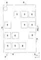
- FIG. 3 is a drawing of power/ground layer 140 as described in various representative embodiments of the present patent document.
- FIG. 3 shows only a part of the power/ground layer 140 of the laminate 110 of the example of FIG. 2 .
- the power/ground layer 140 comprises the electrically conducting area 165 and multiple open areas 170 .
- the open areas each have a centroid 171 , only one of which is shown in FIG. 3 for clarity of illustration.
- the open areas 170 in a typical application have a repeating size, a repeating shape, and a repeating orientation with respect to a Cartesian coordinate system 178 , and the open areas 170 are interspersed inside an outer perimeter 180 of the electrically conducting area 165 .
- the opening for via 160 in the power/ground layer 140 is also shown.
- FIG. 4 is a drawing of overlaid layers as described in various representative embodiments of the present patent document. Shown in FIG. 4 is the power/ground layer 140 of the example of FIG. 3 which is only a part of the example of FIG. 2 . Also, shown overlaying the power/ground layer 140 is solder bump 125 bonded to solder bump pad 185 attached to trace 155 on the first signal layer 130 . The opposite end of trace 155 is connected to a capture pad 190 , also referred to as a land 190 , that connects to the via 160 which is then connected to a series of additional traces and vias to provide electrical connection to one of the package pins 115 . In FIG. 4, as well as FIG. 2, the trace 155 overlays several open areas 170 .
- FIG. 5 is another drawing of power/ground layer 140 as described in various representative embodiments of the present patent document.
- an effective return path 156 on the power/ground layer 140 for the signal carried by the trace 155 on the first signal layer 130 is shown. Note that this effective return path 156 is longer than it would be if the trace 155 did not overlay the open areas 170 .
- FIG. 6 is another drawing of the cross-section of the integrated circuit package 100 as described in various representative embodiments of the present patent document.
- the interconnecting laminate 110 comprises the first signal layer 130 , the first insulating layer 135 , the power/ground layer 140 , the second insulating layer 145 , and the second signal layer 150 . These top layers rest on the core 175 . On the opposite side of the core there are additional laminate layers 195 .
- the solder bumps 125 are soldered to pads 185 on the surface of the laminate substrate 110 .
- the pads 185 then connect to electrically conducting traces 155 on the first signal layer 130 .
- the combination of traces 155 and vias 160 provides a path for the signal to traverse through the layers 130 , 135 , 140 , 145 , 150 , 175 , 195 to make contact with the package pins 115 .
- the power/ground layer 140 comprises the electrically conducting area 165 and open areas 170 .
- open areas 170 are located so that they do not lie directly over trace 155 on second signal layer 150
- open areas 170 are located so that they do not lie directly under trace 155 located on first signal layer 130 .
- the construct of FIG. 6 results in very good shielding between the two traces 155 with associated relatively reduced cross-talk.
- FIG. 7 is yet another drawing of the power/ground layer 140 as described in various representative embodiments of the present patent document.
- FIG. 7 shows only a part of the power/ground layer 140 of the laminate 110 of the example of FIG. 6 .
- the power/ground layer 140 comprises the electrically conducting area 165 and multiple open areas 170 .
- the open areas 170 generally have a repeating size, a repeating shape, and a repeating orientation with respect to the Cartesian coordinate system 178 , and the open areas 170 are interspersed inside the outer perimeter 180 of the electrically conducting area 165 .
- the opening for via 160 in the power/ground layer 140 is also shown.
- open areas 170 may be random in both shape, size, and/or placement, or they may be repeating in shape and/or size with or without being regular in their placement.
- the percentage of the power/ground layer 140 consumed by the open areas 170 will be preferably greater than or equal to 10% and less than or equal to 30%.
- FIG. 8 is another drawing of overlaid layers as described in various representative embodiments of the present patent document. Shown in FIG. 8 is the power/ground layer 140 of the example of FIG. 7 which is only a part of the example of FIG. 6 . Also, shown overlaying the power/ground layer 140 is solder bump 125 bonded to solder bump pad 185 attached to trace 155 on the first signal layer 130 . The opposite end of trace 155 connected to capture pad 190 that connects to the via 160 which is then connected to a series of additional traces and vias to provide electrical connection to one of the package pins 115 . Note that in FIG. 8, as well as FIG. 6, the trace 155 on first signal layer 130 overlays only electrically conducting area 165 on the power/ground layer 140 . As stated above, the construct of FIGS. 5, 6 , and 7 results in very good shielding between the two traces 155 with associated relatively reduced cross-talk talk.
- the effective inductance and resistance of traces for the first example of FIGS. 2 and 4 is greater than that for the traces 155 and power/ground layer 140 return path of the second example of FIGS. 6 and 8 which would result in a greater delay time and thus speed of the packaged integrated circuit 105 .
- FIG. 9 is a drawing of a topside view of overlaid layers as described in various representative embodiments of the present patent document.
- multiple traces 155 on first and second signal layers 130 , 150 originating from closely spaced end points, as for example neighbor solder bumps 125 , and terminating on more widely spaced end points, as for example, package pins 115 would form a radial appearing pattern on both signal layers 130 , 150 and on power/ground layer 140 .
- a primary advantage of the embodiment as described in the present patent document over prior techniques for the construction of power/ground layers 140 in interconnecting laminate 110 for integrated circuit chips 105 is the reduction in cross-talk between signal layers 130 , 150 lying on opposite sides of the power/ground layer 140 .
- a further advantage is the reduction in the effective resistance and inductance of the interconnecting traces 155 .
Landscapes
- Physics & Mathematics (AREA)
- Electromagnetism (AREA)
- Engineering & Computer Science (AREA)
- Microelectronics & Electronic Packaging (AREA)
- Production Of Multi-Layered Print Wiring Board (AREA)
Abstract
Description
Claims (21)
Priority Applications (1)
| Application Number | Priority Date | Filing Date | Title |
|---|---|---|---|
| US10/072,261 US6630628B2 (en) | 2002-02-07 | 2002-02-07 | High-performance laminate for integrated circuit interconnection |
Applications Claiming Priority (1)
| Application Number | Priority Date | Filing Date | Title |
|---|---|---|---|
| US10/072,261 US6630628B2 (en) | 2002-02-07 | 2002-02-07 | High-performance laminate for integrated circuit interconnection |
Publications (2)
| Publication Number | Publication Date |
|---|---|
| US20030148077A1 US20030148077A1 (en) | 2003-08-07 |
| US6630628B2 true US6630628B2 (en) | 2003-10-07 |
Family
ID=27659435
Family Applications (1)
| Application Number | Title | Priority Date | Filing Date |
|---|---|---|---|
| US10/072,261 Expired - Fee Related US6630628B2 (en) | 2002-02-07 | 2002-02-07 | High-performance laminate for integrated circuit interconnection |
Country Status (1)
| Country | Link |
|---|---|
| US (1) | US6630628B2 (en) |
Cited By (3)
| Publication number | Priority date | Publication date | Assignee | Title |
|---|---|---|---|---|
| US20040147165A1 (en) * | 2002-11-20 | 2004-07-29 | Brian Celella | Apparatus for crosstalk compensation in a telecommunications connector |
| US20040196682A1 (en) * | 2002-09-26 | 2004-10-07 | Elpida Memory, Inc. | Semiconductor unit having two device terminals for every one input/output signal |
| US20090106976A1 (en) * | 2007-10-25 | 2009-04-30 | International Business Machines Corporation | Method for reducing noise coupling in high speed digital systems |
Families Citing this family (2)
| Publication number | Priority date | Publication date | Assignee | Title |
|---|---|---|---|---|
| US7492605B2 (en) * | 2006-06-22 | 2009-02-17 | Intel Corporation | Power plane to reduce voltage difference between connector power pins |
| JP6324738B2 (en) * | 2014-01-27 | 2018-05-16 | ルネサスエレクトロニクス株式会社 | Semiconductor device |
Citations (7)
| Publication number | Priority date | Publication date | Assignee | Title |
|---|---|---|---|---|
| US5446243A (en) * | 1992-05-20 | 1995-08-29 | International Business Machines Corporation | Post processing shielding |
| US5856913A (en) * | 1996-04-29 | 1999-01-05 | Semikron Elektronik Gmbh | Multilayer semiconductor device having high packing density |
| US6184478B1 (en) * | 1998-09-30 | 2001-02-06 | Adtec Corporation | Printed wiring device with base layer having a grid pattern |
| US6184477B1 (en) * | 1998-12-02 | 2001-02-06 | Kyocera Corporation | Multi-layer circuit substrate having orthogonal grid ground and power planes |
| US6218631B1 (en) * | 1998-05-13 | 2001-04-17 | International Business Machines Corporation | Structure for reducing cross-talk in VLSI circuits and method of making same using filled channels to minimize cross-talk |
| US6255600B1 (en) * | 1993-03-01 | 2001-07-03 | The Board Of Trustees Of The University Of Arkansas | Electronic interconnection medium having offset electrical mesh plane |
| US6441470B1 (en) * | 2001-08-21 | 2002-08-27 | Sun Microsystems, Inc. | Technique to minimize crosstalk in electronic packages |
-
2002
- 2002-02-07 US US10/072,261 patent/US6630628B2/en not_active Expired - Fee Related
Patent Citations (7)
| Publication number | Priority date | Publication date | Assignee | Title |
|---|---|---|---|---|
| US5446243A (en) * | 1992-05-20 | 1995-08-29 | International Business Machines Corporation | Post processing shielding |
| US6255600B1 (en) * | 1993-03-01 | 2001-07-03 | The Board Of Trustees Of The University Of Arkansas | Electronic interconnection medium having offset electrical mesh plane |
| US5856913A (en) * | 1996-04-29 | 1999-01-05 | Semikron Elektronik Gmbh | Multilayer semiconductor device having high packing density |
| US6218631B1 (en) * | 1998-05-13 | 2001-04-17 | International Business Machines Corporation | Structure for reducing cross-talk in VLSI circuits and method of making same using filled channels to minimize cross-talk |
| US6184478B1 (en) * | 1998-09-30 | 2001-02-06 | Adtec Corporation | Printed wiring device with base layer having a grid pattern |
| US6184477B1 (en) * | 1998-12-02 | 2001-02-06 | Kyocera Corporation | Multi-layer circuit substrate having orthogonal grid ground and power planes |
| US6441470B1 (en) * | 2001-08-21 | 2002-08-27 | Sun Microsystems, Inc. | Technique to minimize crosstalk in electronic packages |
Cited By (9)
| Publication number | Priority date | Publication date | Assignee | Title |
|---|---|---|---|---|
| US20040196682A1 (en) * | 2002-09-26 | 2004-10-07 | Elpida Memory, Inc. | Semiconductor unit having two device terminals for every one input/output signal |
| US7633147B2 (en) * | 2002-09-26 | 2009-12-15 | Elpida Memory, Inc. | Semiconductor unit having two device terminals for every one input/output signal |
| US20040147165A1 (en) * | 2002-11-20 | 2004-07-29 | Brian Celella | Apparatus for crosstalk compensation in a telecommunications connector |
| WO2004047240A3 (en) * | 2002-11-20 | 2004-12-09 | Siemon Co | Apparatus for crosstalk compensation in a telecommunications connector |
| US7154049B2 (en) | 2002-11-20 | 2006-12-26 | The Siemon Company | Apparatus for crosstalk compensation in a telecommunications connector |
| US20090106976A1 (en) * | 2007-10-25 | 2009-04-30 | International Business Machines Corporation | Method for reducing noise coupling in high speed digital systems |
| US20090107705A1 (en) * | 2007-10-25 | 2009-04-30 | International Business Machines Corporation | Methods and systems for reducing noise coupling in high speed digital systems |
| US7533458B1 (en) * | 2007-10-25 | 2009-05-19 | International Business Machines Corporation | Method for reducing noise coupling in high speed digital systems |
| US8084692B2 (en) | 2007-10-25 | 2011-12-27 | International Business Machines Corporation | Reducing noise coupling in high speed digital systems |
Also Published As
| Publication number | Publication date |
|---|---|
| US20030148077A1 (en) | 2003-08-07 |
Similar Documents
| Publication | Publication Date | Title |
|---|---|---|
| US6888240B2 (en) | High performance, low cost microelectronic circuit package with interposer | |
| US6796028B2 (en) | Method of Interconnecting substrates for electrical coupling of microelectronic components | |
| US5471090A (en) | Electronic structures having a joining geometry providing reduced capacitive loading | |
| US9548279B2 (en) | Connection member, semiconductor device, and stacked structure | |
| US7754538B2 (en) | Packaging substrate structure with electronic components embedded therein and method for manufacturing the same | |
| US9024447B2 (en) | Stackable electronic package and method of making same | |
| US11967587B2 (en) | IC package with top-side memory module | |
| US6747356B2 (en) | Semiconductor device | |
| US8675369B2 (en) | Module board | |
| US6750403B2 (en) | Reconfigurable multilayer printed circuit board | |
| KR101481571B1 (en) | Semiconductor Package apparatus and its manufacturing method | |
| US20150282328A1 (en) | Communication module | |
| US6630628B2 (en) | High-performance laminate for integrated circuit interconnection | |
| US6657295B2 (en) | Multilayer interconnect board and multilayer semiconductor device | |
| US8063481B2 (en) | High-speed memory package | |
| US11088123B1 (en) | Package system having laterally offset and ovelapping chip packages | |
| JP4128440B2 (en) | Built-in module | |
| JP2008283114A (en) | Electronic component mounting wiring board and method for removing electromagnetic noise from electronic component mounting wiring board | |
| US20080116587A1 (en) | Conductor polymer composite carrier with isoproperty conductive columns | |
| JPH0553269U (en) | Multilayer wiring board with high-frequency shield structure | |
| JP2001144207A (en) | Multilayer wiring board and semiconductor device | |
| JPH09306950A (en) | Semiconductor device, mounting board and mounting method | |
| Shiroshita et al. | Electrical Performance of Advanced Surface Laminar Circuit in High-end FCBGA Applications | |
| JP2002368186A (en) | Semiconductor device | |
| CN115763437A (en) | System-level electromagnetic shielding packaging structure, preparation method and electronic product |
Legal Events
| Date | Code | Title | Description |
|---|---|---|---|
| AS | Assignment |
Owner name: AGILENT TECHNOLOGIES, INC., COLORADO Free format text: ASSIGNMENT OF ASSIGNORS INTEREST;ASSIGNORS:DEVNANI, NURWATI S.;BURTON, WILLIAM S.;CHRISTENSEN, SARI K.;REEL/FRAME:012930/0605 Effective date: 20020205 |
|
| AS | Assignment |
Owner name: AVAGO TECHNOLOGIES GENERAL IP PTE. LTD., SINGAPORE Free format text: ASSIGNMENT OF ASSIGNORS INTEREST;ASSIGNOR:AGILENT TECHNOLOGIES, INC.;REEL/FRAME:017207/0020 Effective date: 20051201 |
|
| REMI | Maintenance fee reminder mailed | ||
| LAPS | Lapse for failure to pay maintenance fees | ||
| STCH | Information on status: patent discontinuation |
Free format text: PATENT EXPIRED DUE TO NONPAYMENT OF MAINTENANCE FEES UNDER 37 CFR 1.362 |
|
| FP | Lapsed due to failure to pay maintenance fee |
Effective date: 20071007 |
|
| AS | Assignment |
Owner name: AVAGO TECHNOLOGIES GENERAL IP (SINGAPORE) PTE. LTD., SINGAPORE Free format text: CORRECTIVE ASSIGNMENT TO CORRECT THE NAME OF THE ASSIGNEE PREVIOUSLY RECORDED ON REEL 017207 FRAME 0020. ASSIGNOR(S) HEREBY CONFIRMS THE ASSIGNMENT;ASSIGNOR:AGILENT TECHNOLOGIES, INC.;REEL/FRAME:038633/0001 Effective date: 20051201 Owner name: AVAGO TECHNOLOGIES GENERAL IP (SINGAPORE) PTE. LTD Free format text: CORRECTIVE ASSIGNMENT TO CORRECT THE NAME OF THE ASSIGNEE PREVIOUSLY RECORDED ON REEL 017207 FRAME 0020. ASSIGNOR(S) HEREBY CONFIRMS THE ASSIGNMENT;ASSIGNOR:AGILENT TECHNOLOGIES, INC.;REEL/FRAME:038633/0001 Effective date: 20051201 |