US6580275B2 - Single sensor control of power converters - Google Patents

Single sensor control of power converters Download PDF

Info

Publication number
US6580275B2
US6580275B2 US09/870,408 US87040801A US6580275B2 US 6580275 B2 US6580275 B2 US 6580275B2 US 87040801 A US87040801 A US 87040801A US 6580275 B2 US6580275 B2 US 6580275B2
Authority
US
United States
Prior art keywords
inductor
voltage
current
lamp
determining
Prior art date
Legal status (The legal status is an assumption and is not a legal conclusion. Google has not performed a legal analysis and makes no representation as to the accuracy of the status listed.)
Expired - Lifetime
Application number
US09/870,408
Other versions
US20020030493A1 (en
Inventor
Shu-Yuen Ron Hui
Shu-Hung Henry Chung
Current Assignee (The listed assignees may be inaccurate. Google has not performed a legal analysis and makes no representation or warranty as to the accuracy of the list.)
City University of Hong Kong CityU
Original Assignee
City University of Hong Kong CityU
Priority date (The priority date is an assumption and is not a legal conclusion. Google has not performed a legal analysis and makes no representation as to the accuracy of the date listed.)
Filing date
Publication date
Application filed by City University of Hong Kong CityU filed Critical City University of Hong Kong CityU
Priority to US09/870,408 priority Critical patent/US6580275B2/en
Assigned to CITY UNIVERSITY OF HONG KONG reassignment CITY UNIVERSITY OF HONG KONG ASSIGNMENT OF ASSIGNORS INTEREST (SEE DOCUMENT FOR DETAILS). Assignors: CHUNG, SHU-HUNG HENRY, HUI, SHU-YUEN RON
Publication of US20020030493A1 publication Critical patent/US20020030493A1/en
Application granted granted Critical
Publication of US6580275B2 publication Critical patent/US6580275B2/en
Anticipated expiration legal-status Critical
Expired - Lifetime legal-status Critical Current

Links

Images

Classifications

    • HELECTRICITY
    • H05ELECTRIC TECHNIQUES NOT OTHERWISE PROVIDED FOR
    • H05BELECTRIC HEATING; ELECTRIC LIGHT SOURCES NOT OTHERWISE PROVIDED FOR; CIRCUIT ARRANGEMENTS FOR ELECTRIC LIGHT SOURCES, IN GENERAL
    • H05B41/00Circuit arrangements or apparatus for igniting or operating discharge lamps
    • H05B41/14Circuit arrangements
    • H05B41/36Controlling
    • GPHYSICS
    • G01MEASURING; TESTING
    • G01RMEASURING ELECTRIC VARIABLES; MEASURING MAGNETIC VARIABLES
    • G01R31/00Arrangements for testing electric properties; Arrangements for locating electric faults; Arrangements for electrical testing characterised by what is being tested not provided for elsewhere
    • G01R31/24Testing of discharge tubes
    • G01R31/245Testing of gas discharge tubes
    • HELECTRICITY
    • H05ELECTRIC TECHNIQUES NOT OTHERWISE PROVIDED FOR
    • H05BELECTRIC HEATING; ELECTRIC LIGHT SOURCES NOT OTHERWISE PROVIDED FOR; CIRCUIT ARRANGEMENTS FOR ELECTRIC LIGHT SOURCES, IN GENERAL
    • H05B41/00Circuit arrangements or apparatus for igniting or operating discharge lamps
    • H05B41/14Circuit arrangements
    • H05B41/26Circuit arrangements in which the lamp is fed by power derived from dc by means of a converter, e.g. by high-voltage dc
    • H05B41/28Circuit arrangements in which the lamp is fed by power derived from dc by means of a converter, e.g. by high-voltage dc using static converters
    • H05B41/282Circuit arrangements in which the lamp is fed by power derived from dc by means of a converter, e.g. by high-voltage dc using static converters with semiconductor devices
    • H05B41/2825Circuit arrangements in which the lamp is fed by power derived from dc by means of a converter, e.g. by high-voltage dc using static converters with semiconductor devices by means of a bridge converter in the final stage
    • HELECTRICITY
    • H05ELECTRIC TECHNIQUES NOT OTHERWISE PROVIDED FOR
    • H05BELECTRIC HEATING; ELECTRIC LIGHT SOURCES NOT OTHERWISE PROVIDED FOR; CIRCUIT ARRANGEMENTS FOR ELECTRIC LIGHT SOURCES, IN GENERAL
    • H05B41/00Circuit arrangements or apparatus for igniting or operating discharge lamps
    • H05B41/14Circuit arrangements
    • H05B41/26Circuit arrangements in which the lamp is fed by power derived from dc by means of a converter, e.g. by high-voltage dc
    • H05B41/28Circuit arrangements in which the lamp is fed by power derived from dc by means of a converter, e.g. by high-voltage dc using static converters
    • H05B41/282Circuit arrangements in which the lamp is fed by power derived from dc by means of a converter, e.g. by high-voltage dc using static converters with semiconductor devices
    • H05B41/285Arrangements for protecting lamps or circuits against abnormal operating conditions
    • H05B41/2851Arrangements for protecting lamps or circuits against abnormal operating conditions for protecting the circuit against abnormal operating conditions
    • H05B41/2855Arrangements for protecting lamps or circuits against abnormal operating conditions for protecting the circuit against abnormal operating conditions against abnormal lamp operating conditions
    • HELECTRICITY
    • H05ELECTRIC TECHNIQUES NOT OTHERWISE PROVIDED FOR
    • H05BELECTRIC HEATING; ELECTRIC LIGHT SOURCES NOT OTHERWISE PROVIDED FOR; CIRCUIT ARRANGEMENTS FOR ELECTRIC LIGHT SOURCES, IN GENERAL
    • H05B41/00Circuit arrangements or apparatus for igniting or operating discharge lamps
    • H05B41/14Circuit arrangements
    • H05B41/36Controlling
    • H05B41/38Controlling the intensity of light
    • H05B41/39Controlling the intensity of light continuously
    • H05B41/392Controlling the intensity of light continuously using semiconductor devices, e.g. thyristor
    • H05B41/3921Controlling the intensity of light continuously using semiconductor devices, e.g. thyristor with possibility of light intensity variations
    • H05B41/3925Controlling the intensity of light continuously using semiconductor devices, e.g. thyristor with possibility of light intensity variations by frequency variation

Definitions

  • This invention relates to methods and apparatus for the control of power converters and the like circuitry, and particular to methods and apparatus for such control that do not require direct sensing of input and/or output voltages.
  • the invention relates in particular to methods and apparatus for determining the operating characteristics of a discharge lamp (for example a fluorescent discharge lamp or a high-intensity discharge lamp) such as lamp power, lamp resistance and input voltage.
  • a discharge lamp for example a fluorescent discharge lamp or a high-intensity discharge lamp
  • Switching power converters are widely used in a large number of domestic and industrial applications. Examples include computer systems, motor drivers, and uninterruptible power supplies. With recent advances in semiconductor technologies and electronic packaging techniques, much research has been done on new power circuit topologies, switching scheme, and control techniques for improving the converter efficiency, electrical specifications, and power density—all the time meeting various industrial standards. Examples of well known power converter topologies include buck converters, boost converters, buck boost converters, flyback converters and forward converters.
  • the current can be sensed using a contactless flux linkage sensor such as a Hall effect sensor, electrical isolation between the power conversion stage and the control state may be achieved easily. This has the effect that the power and ground signals can be separated inherently so as to reduce noise coupling.
  • apparatus for determining the characteristic(s) of a discharge lamp operated by a high-frequency electronic ballast including a resonant tank comprising an inductor and a capacitor, wherein said characteristic(s) are selected from the group consisting of lamp input voltage, lamp resistance and lamp power, comprising means for measuring the inductor voltage and/or current, and means for determining said characteristic(s) from the measured inductor voltage and/or current.
  • control variables such as input and output voltages
  • characteristics of the load such as a discharge lamp
  • the control variables such as input and output voltages
  • the characteristics of the load such as a discharge lamp
  • any significant changes in the lamp resistance may indicate lamp instability or failure, and since by means of the present invention the lamp resistance can be monitored remotely through measurements of the inductor voltage or current, the lamp resistance can be monitored remotely to identify any instability or failure.
  • the present invention may be employed to detect load condition to facilitate load monitoring (for stability control for example).
  • the apparatus may comprise means for obtaining the lamp current and the maximum inductor voltage from the measured inductor voltage and/or current, and the characteristic(s) determining means may then determine the characteristics from the lamp current and maximum inductor voltage.
  • the apparatus comprises a sensor for measuring the inductor voltage, means for differentiating the inductor voltage to obtain a capacitor current, means for integrating the inductor voltage to obtain an inductor current, means for obtaining the lamp current from the capacitor current and the inductor current, and peak detector means for detecting the maximum inductor voltage.
  • the apparatus comprises a sensor for measuring inductor current, means for differentiating the inductor current to obtain an inductor voltage, means for differentiating the inductor voltage to obtain an capacitor current, means for obtaining the lamp current from the capacitor current and the inductor current, and peak detector means for detecting the maximum inductor voltage.
  • the present invention provides apparatus for determining the lamp power, lamp resistance and input voltage of a discharge lamp driven by a power converter circuit including an inductor, comprising means for measuring the inductor voltage or inductor current, and means for determining the lamp power, lamp resistance and/or input voltage from said measured inductor voltage or inductor current.
  • the invention provides a method for determining the characteristic(s) of a discharge lamp operated by a high-frequency electronic ballast including a resonant tank comprising an inductor and a capacitor, wherein said characteristic(s) are selected from the group consisting of lamp input voltage, lamp resistance and lamp power, comprising measuring the inductor voltage and/or current, and determining said characteristic(s) from the measured inductor voltage and/or current.
  • the present invention provides apparatus for determining the input and/or output voltages of a power electronics converter circuit including an inductor, comprising means for sensing the voltage across the inductor, and means for calculating the input and output voltages from the inductor voltage.
  • the apparatus may also be able to calculate the load resistance from the inductor voltage.
  • FIG. 1 illustrates the basic principle of the present invention
  • FIG. 2 is a circuit diagram of a first embodiment of the invention in the form of a series-loaded parallel-resonant inverter
  • FIGS. 3 ( a )-( c ) show the key waveforms of the inverter of FIG. 2 in one switching cycle
  • FIG. 4 shows ( a ) a typical electronic ballast circuit and ( b ) its equivalent circuit
  • FIG. 5 shows the relationship between ( a ) lamp power and DC link voltage and ( b ) lamp power and lamp resistance for a typical fluorescent lamp
  • FIG. 6 is a plot of ( a ) transfer function against load, and ( b ) output voltage error under different loads showing the effect of harmonic components,
  • FIG. 7 is a plot of ( a ) voltage and ( b ) current simulation curves
  • FIG. 8 is a plot showing the relationship between lamp current and maximum lamp voltage
  • FIG. 9 is a plot showing the relationship between lamp current, maximum lamp voltage and lamp resistance
  • FIG. 10 is ( a ) a circuit digram of a second embodiment and ( b ) a third embodiment of the present invention.
  • FIG. 11 is a plot of estimated and measured ( a ) input voltage against lamp power, ( b ) lamp resistance against lamp power and ( c ) lamp power, of the second embodiment of the invention.
  • the present invention involves the use of an isolated or non-isolated voltage sensor to obtain the voltage across an inductor that forms part of a power electronic converter.
  • the measured voltage may be used to determine the AC current flowing in the inductor, and from that a number of other variables, such as the input and output voltages, can be determined.
  • FIG. 1 shows the basic idea.
  • L is the inductance of the inductor and i L is the AC component of the inductor current I L . It can be seen from this relationship that the AC current flowing through an inductor can be obtained by integrating the sensed inductor voltage, and thus that a single voltage sensor can give both the voltage and current information. Thus the number of sensors needed can be reduced.
  • FIG. 2 shows a first embodiment of this invention in the form of a series-loaded parallel resonant inverter, as is used for example in applications such as electronic ballasts.
  • An input voltage V dc is applied and the lamp may be considered as an output load R.
  • FIGS. 3 ( a )-( c ) show the key waveforms in one switching cycle of the converter.
  • the gate signals of all the switches ie S 1 -S 4 ) are controlled by either v g1 or v g2 . As shown in FIG.
  • V dc v L ( T + )+ v out ( T + ) (2)
  • V dc can also be determined by subtracting (1) from (2) so that
  • V dc ⁇ 1 ⁇ 2 [v L ( T + ) ⁇ v L ( T ⁇ )]
  • both the input and output voltages can be determined from a measurement of only the inductor voltage, and thus only a single sensor is required in order to determine both the input and output voltage.
  • the input and output voltages can be derived by synchronizing the sample-and-hold (S/H) circuit with the gate signals. This is shown in FIG. 2 in which it will be seen that the gate voltage v g2 not only controls the switches but also controls the S/H circuit so that the inductor voltage is sampled and held at the switching instant.
  • the inductor voltage will in fact be varying with the switching frequency it must be subject to amplitude demodulation using amplitude modulation demodulator circuits (AMD) capable of demodulating non-sinusoidal time-varying pulses of fixed frequency.
  • AMD amplitude modulation demodulator circuits
  • an integrating circuit is used to integrate the inductor voltage to obtain the inductor current which is fed to a S/H circuit also controlled by the gate voltage.
  • a second embodiment of the invention will now be described in which the resistance of a discharge lamp operated by a high-frequency electronic ballast may be monitored.
  • the lamp resistance varies with the dimming level. This resistance is difficult to detect directly in real time, but using the single sensor principle of the present invention and a simple circuit design it is possible to estimate with a reasonable degree of accuracy the on-line characteristic.
  • a single sensor is used to derive the load resistance (R), the load power (P), load voltage V OUT and the DC link voltage (V DC ).
  • FIG. 4 ( a ) shows a typical electronic ballast circuit as is commonly used for a discharge lamp.
  • FIG. 4 ( b ) shows the equivalent circuit.
  • Two switches S 1 and S 3 are switched alternately in order to generate an ac rectangular voltage across the load.
  • the dc blocking capacitor C DC eliminates the dc voltage so that only the ac voltage component is applied across the resonant tank (formed of L and C) and the load (ie the discharge lamp in this example).
  • FIGS. 5 ( a ) and ( b ) show typical lamp characteristics of a GEC 40W-SW fluorescent lamp as a function of lamp power when driven by a circuit such as that of FIG. 4 ( a ).
  • V DC is the RMS value of v s (t) and is named as the DC link voltage from now on
  • ⁇ s is the angular switching frequency
  • ⁇ s 2 ⁇ /T s .
  • V OUT1 4 ⁇ V DC 2 ⁇ ⁇ ⁇ R ( ⁇ S ⁇ L ) 2 + R 2 ⁇ ( ⁇ S ⁇ L ⁇ ⁇ ⁇ S ⁇ C - 1 ) 2 ( 8 )
  • H(1) is the transfer function of the fundamental component.
  • H(n) is the transfer function of the n th harmonic component.
  • the fluorescent lamp resistance varies from about 300 ⁇ to 3 k ⁇ between lamp power's range—[36 W, 6 W].
  • the fluorescent lamp may be replaced by a resistor R.
  • the RMS value of output voltage V OUT is taken and compared with the calculated value (14).
  • the resistance equals to 400 ⁇ , 1 k ⁇ and 3 k ⁇ respectively, the absolute error of V OUT is shown in FIG. 6 ( b ), the maximum error is about 2% when V DC changes from 40V to 120V.
  • the high accuracy confirms that the calculation of V OUT (14) is feasible.
  • V DC v L ( t 0 )+ v OUT ( t 0 )
  • I RMAX ⁇ square root over (2) ⁇ I R (20)
  • FIG. 8 shows the relationship between I R and V LMAX under different R when V DC changes from 40V to 120V.
  • Different R has its unique slope of I R and V LMAX , the slope stands for the value of resistance indirectly.
  • K ⁇ ( R ) 2 4 ⁇ ⁇ ⁇ ( ⁇ S ⁇ L ) 2 + R 2 ⁇ ( ⁇ S 2 ⁇ LC - 1 ) 2 + 2 ⁇ R ( 23 )
  • the output power can be defined by
  • the on-line lamp characteristic can be defined by (24), (26) and (27) after obtaining V LMAX and I R .
  • the single-sensor principle can be implemented either using a voltage or a current sensor as shown in FIG. 10 .
  • a voltage sensor for sensing the inductor voltage v L .
  • a current sensor e.g. Hall-effect current sensor
  • inductor current i L is used to get inductor current i L .
  • the single-sensor principle is demonstrated by the single voltage sensor approach.
  • the scale-down inductor voltage v L (t) can be obtained by an extra coupled winding on the inductor.
  • the estimated maximum inductor voltage i.e., V LMAX
  • the estimated output current I R can be obtained by sampling and holding i L (t) at t 0 . Therefore, not only the resistance but also the output power and DC link voltage can be estimated at the same time by estimating the inductor voltage.
  • a current transducer is used to obtain the scale-down inductor current i L (t).
  • v L (t) comes from differentiating i L (t), V LMAX and I R can be obtained by the similar technique in FIG. 9 ( a ).
  • FIGS. 11 ( a )-( c ) show the measured and estimated values of the dc link voltage V DC , lamp resistance R lamp and lamp power P lamp , respectively.
  • the dotted lines represent the measurements and the solid lines represent the estimations using the single voltage sensor approach as shown in FIG. 9 ( a ). The estimations are found to be consistant with measurements.
  • the present invention has been illustrated above by means of an example in the form of a fluorescent discharge lamp.
  • the present invention is also applicable to other forms of discharge lamps such as high intensity discharge (HID) lamps.
  • HID high intensity discharge
  • the present invention may be particularly useful in the context of HID lamps because they can suffer from are vibration problems.
  • the stability of such an HID lamp may be monitored and controlled.

Landscapes

  • Physics & Mathematics (AREA)
  • General Physics & Mathematics (AREA)
  • Circuit Arrangements For Discharge Lamps (AREA)

Abstract

An apparatus and method for determining the characteristic(s) of a discharge lamp (for example a fluorescent lamp or a high-intensity discharge lamp) operated by a high-frequency electronic ballast including a resonant tank that includes an inductor and a capacitor, wherein the characteristic(s) are selected from the group consisting of lamp input voltage, lamp resistance and lamp power, and including capability for measuring the inductor voltage and/or current, and capability for determining the characteristic(s) from the measured inductor voltage and/or current. More generally, the apparatus and method provide techniques for determining a number of parameters of a power converter circuit simply from measuring an inductor voltage or inductor current.

Description

This application claims the benefit of U.S. Provisional Application No. 60/208,343 filed May 31, 2000, entitled SINGLE VOLTAGE SENSOR CONTROL OF POWER CONVERTERS, and which is in its entirety incorporated herewith by reference.
FIELD OF THE INVENTION
This invention relates to methods and apparatus for the control of power converters and the like circuitry, and particular to methods and apparatus for such control that do not require direct sensing of input and/or output voltages. The invention relates in particular to methods and apparatus for determining the operating characteristics of a discharge lamp (for example a fluorescent discharge lamp or a high-intensity discharge lamp) such as lamp power, lamp resistance and input voltage.
BACKGROUND OF THE INVENTION
Switching power converters are widely used in a large number of domestic and industrial applications. Examples include computer systems, motor drivers, and uninterruptible power supplies. With recent advances in semiconductor technologies and electronic packaging techniques, much research has been done on new power circuit topologies, switching scheme, and control techniques for improving the converter efficiency, electrical specifications, and power density—all the time meeting various industrial standards. Examples of well known power converter topologies include buck converters, boost converters, buck boost converters, flyback converters and forward converters.
An underlying concept of power electronics is to be able to use low-level signals to control high power converter outputs. Conventionally this requires a comparison of the actual output voltage with a desired reference voltage and then giving commands to the power converters. However, it is common practice that the power conversion stage and the control circuit be isolated in order to avoid noise coupling and grounding problems. In some situations input and output isolation in the power conversion stage is also desirable or necessary. These isolation requirements means that signal-power interface techniques such as transformer coupling and optical isolation are necessary to achieve output regulation. These requirements substantially increase the cost and complexity of power converters.
PRIOR ART
One solution to this difficulty is to control switching power converters by using current sensors only and without requiring the use of voltage sensors. Such a system was described in T. Ohnuki, O. Miyashita, P. Lataire & G. Matson IEEE Transactions on Power Electronics, Vol. 14 No. 2 March 1999. In the system proposed in this paper only current sensors are used that generate signals in response to the currents flowing in inductors. The sensed current can in theory be used to obtain the input and output voltages so as to provide control information. The use of current sensors alone has a number of advantages including a reduction in the number of sensors needed, and it obviates the need to use a dissipative voltage divider, such as a resistive network, to obtain the input voltage in feedforward arrangements and in output voltage regulation. Additionally, no voltage isolator (such as an optical coupler) is needed to isolate the high-voltage output and the low-voltage control signals. This has an additional advantage in that some optical isolators have a finite linear range, eliminating the need for such isolators therefore increases the practical voltage measurement range.
Since the current can be sensed using a contactless flux linkage sensor such as a Hall effect sensor, electrical isolation between the power conversion stage and the control state may be achieved easily. This has the effect that the power and ground signals can be separated inherently so as to reduce noise coupling.
The proposal of this piece of prior art has, however, a number of practical drawbacks. Most importantly, it assumes that the circuit is an ideal circuit, which in reality no such circuit ever would be. In addition, the current rather than being continuously sensed is simply sampled once in every switching cycle with the inevitable approximations and inaccuracies that this implies. An improvement on this technique is disclosed in the Applicants application Ser. No. 09/524,041, U.S. Pat. No. 6,297,621, which is incorporated herein by reference.
SUMMARY OF THE INVENTION
According to the present invention there is provided apparatus for determining the characteristic(s) of a discharge lamp operated by a high-frequency electronic ballast including a resonant tank comprising an inductor and a capacitor, wherein said characteristic(s) are selected from the group consisting of lamp input voltage, lamp resistance and lamp power, comprising means for measuring the inductor voltage and/or current, and means for determining said characteristic(s) from the measured inductor voltage and/or current.
By means of this invention, at least in its preferred forms, the control variables (such as input and output voltages) and the characteristics of the load (such as a discharge lamp) may be obtained more easily than in the prior art. For example, any significant changes in the lamp resistance may indicate lamp instability or failure, and since by means of the present invention the lamp resistance can be monitored remotely through measurements of the inductor voltage or current, the lamp resistance can be monitored remotely to identify any instability or failure. In addition, the present invention may be employed to detect load condition to facilitate load monitoring (for stability control for example).
In preferred embodiments of the invention the apparatus may comprise means for obtaining the lamp current and the maximum inductor voltage from the measured inductor voltage and/or current, and the characteristic(s) determining means may then determine the characteristics from the lamp current and maximum inductor voltage.
In one embodiment the apparatus comprises a sensor for measuring the inductor voltage, means for differentiating the inductor voltage to obtain a capacitor current, means for integrating the inductor voltage to obtain an inductor current, means for obtaining the lamp current from the capacitor current and the inductor current, and peak detector means for detecting the maximum inductor voltage.
In another embodiment the apparatus comprises a sensor for measuring inductor current, means for differentiating the inductor current to obtain an inductor voltage, means for differentiating the inductor voltage to obtain an capacitor current, means for obtaining the lamp current from the capacitor current and the inductor current, and peak detector means for detecting the maximum inductor voltage.
Viewed from another aspect the present invention provides apparatus for determining the lamp power, lamp resistance and input voltage of a discharge lamp driven by a power converter circuit including an inductor, comprising means for measuring the inductor voltage or inductor current, and means for determining the lamp power, lamp resistance and/or input voltage from said measured inductor voltage or inductor current.
Viewed from a still further aspect the invention provides a method for determining the characteristic(s) of a discharge lamp operated by a high-frequency electronic ballast including a resonant tank comprising an inductor and a capacitor, wherein said characteristic(s) are selected from the group consisting of lamp input voltage, lamp resistance and lamp power, comprising measuring the inductor voltage and/or current, and determining said characteristic(s) from the measured inductor voltage and/or current.
More generally still the present invention provides apparatus for determining the input and/or output voltages of a power electronics converter circuit including an inductor, comprising means for sensing the voltage across the inductor, and means for calculating the input and output voltages from the inductor voltage. Preferably the apparatus may also be able to calculate the load resistance from the inductor voltage.
BRIEF DESCRIPTION OF THE DRAWINGS
Some embodiments of the invention will now be described by way of example and with reference to the accompanying drawings, in which:
FIG. 1 illustrates the basic principle of the present invention,
FIG. 2 is a circuit diagram of a first embodiment of the invention in the form of a series-loaded parallel-resonant inverter,
FIGS. 3(a)-(c) show the key waveforms of the inverter of FIG. 2 in one switching cycle,
FIG. 4 shows (a) a typical electronic ballast circuit and (b) its equivalent circuit,
FIG. 5 shows the relationship between (a) lamp power and DC link voltage and (b) lamp power and lamp resistance for a typical fluorescent lamp,
FIG. 6 is a plot of (a) transfer function against load, and (b) output voltage error under different loads showing the effect of harmonic components,
FIG. 7 is a plot of (a) voltage and (b) current simulation curves,
FIG. 8 is a plot showing the relationship between lamp current and maximum lamp voltage,
FIG. 9 is a plot showing the relationship between lamp current, maximum lamp voltage and lamp resistance,
FIG. 10 is (a) a circuit digram of a second embodiment and (b) a third embodiment of the present invention, and
FIG. 11 is a plot of estimated and measured (a) input voltage against lamp power, (b) lamp resistance against lamp power and (c) lamp power, of the second embodiment of the invention.
DETAILED DESCRIPTION OF PREFERRED EMBODIMENTS
The present invention, at least in its preferred forms, involves the use of an isolated or non-isolated voltage sensor to obtain the voltage across an inductor that forms part of a power electronic converter. The measured voltage may be used to determine the AC current flowing in the inductor, and from that a number of other variables, such as the input and output voltages, can be determined.
FIG. 1 shows the basic idea. Mathematically the inductor voltage and the inductor current can be expressed as: v L = L i L I i L = 1 L v L I
Figure US06580275-20030617-M00001
Where L is the inductance of the inductor and iL is the AC component of the inductor current IL. It can be seen from this relationship that the AC current flowing through an inductor can be obtained by integrating the sensed inductor voltage, and thus that a single voltage sensor can give both the voltage and current information. Thus the number of sensors needed can be reduced.
FIG. 2 shows a first embodiment of this invention in the form of a series-loaded parallel resonant inverter, as is used for example in applications such as electronic ballasts. An input voltage Vdc is applied and the lamp may be considered as an output load R. FIGS. 3(a)-(c) show the key waveforms in one switching cycle of the converter. The switching frequency fs (=1Ts) of the switches is slightly higher than the natural frequency of the output resonant tank circuit. The gate signals of all the switches (ie S1-S4) are controlled by either vg1 or vg2. As shown in FIG. 3(a) gate voltages vg1 and vg2 are in an anti-phase relationship. Thus the voltage across the input of the resonant tank circuit is in a square wave form, and in particular there is a voltage change of 2Vdc when the switch pair S1 and S2 is switched into S3 and S4.
The time instant at t=T is considered in the following. By using the Kirchoff voltage law,
V dc =v L(T )+v out(T )  (1)
V dc =v L(T +)+v out(T +)  (2)
As the output voltage vout is relatively constant at the switching instant (vout(T+)≈vout(T), vout at t=T can be determined by adding (1) and (2), that is to say:
−[v out(T +)+v out(T )]=v L(T +)+v L(T )
v out(T)≈−½[v L(T +)+v L(T )]
In addition the input voltage Vdc can also be determined by subtracting (1) from (2) so that
V dc=−½[v L(T +)−v L(T )]
Thus it can be seen that both the input and output voltages can be determined from a measurement of only the inductor voltage, and thus only a single sensor is required in order to determine both the input and output voltage. In particular the input and output voltages can be derived by synchronizing the sample-and-hold (S/H) circuit with the gate signals. This is shown in FIG. 2 in which it will be seen that the gate voltage vg2 not only controls the switches but also controls the S/H circuit so that the inductor voltage is sampled and held at the switching instant. It will also be noted that because the inductor voltage will in fact be varying with the switching frequency it must be subject to amplitude demodulation using amplitude modulation demodulator circuits (AMD) capable of demodulating non-sinusoidal time-varying pulses of fixed frequency. As can also be seen from FIG. 2, an integrating circuit is used to integrate the inductor voltage to obtain the inductor current which is fed to a S/H circuit also controlled by the gate voltage. By obtaining both inductor current and output voltage it is also possible to obtain the load resistance R by dividing the calculated output voltage by the sampled inductor current obtained from integrating the measured inductor voltage.
A second embodiment of the invention will now be described in which the resistance of a discharge lamp operated by a high-frequency electronic ballast may be monitored. When a discharge lamp is being dimmed the lamp resistance varies with the dimming level. This resistance is difficult to detect directly in real time, but using the single sensor principle of the present invention and a simple circuit design it is possible to estimate with a reasonable degree of accuracy the on-line characteristic. In this example, a single sensor is used to derive the load resistance (R), the load power (P), load voltage VOUT and the DC link voltage (VDC).
FIG. 4(a) shows a typical electronic ballast circuit as is commonly used for a discharge lamp. FIG. 4(b) shows the equivalent circuit. Two switches S1 and S3 are switched alternately in order to generate an ac rectangular voltage across the load. The dc blocking capacitor CDC eliminates the dc voltage so that only the ac voltage component is applied across the resonant tank (formed of L and C) and the load (ie the discharge lamp in this example). FIGS. 5(a) and (b) show typical lamp characteristics of a GEC 40W-SW fluorescent lamp as a function of lamp power when driven by a circuit such as that of FIG. 4(a). Before describing an embodiment of the present invention in which the parameters of such a fluorescent lamp may be monitored using a single sensor, it is firstly necessary to consider the theory behind the circuit of FIG. 4(a).
The square wave vs(t) of FIG. 4(b) can be expressed as v S ( t ) = 4 V DC π n = 1 + 1 n sin ( n ω S t ) , n is odd ( 3 )
Figure US06580275-20030617-M00002
where VDC is the RMS value of vs(t) and is named as the DC link voltage from now on, ωs is the angular switching frequency, ωs=2π/Ts.
The relationship between vs(t), vL(t) and vOUT(t) is
v s(t)=v L(t)+v OUT(t)  (4)
v S ( t ) = L i L ( t ) t + v OUT ( t ) = L [ i C ( t ) + i R ( t ) ] t + v OUT ( t ) = LC 2 v OUT ( t ) t 2 + L R v OUT ( t ) t + v OUT ( t ) ( 5 )
Figure US06580275-20030617-M00003
Assume V OUT ( 0 ) t = 0
Figure US06580275-20030617-M00004
and vOUT(0)=0, only consider the fundamental component of vs(t), v S1 ( t ) = 4 V DC π sin ( ω S t ) ( 6 )
Figure US06580275-20030617-M00005
Then the solution of the differential equation (5) is v OUT1 ( t ) = - 4 V DC π R [ ω S L cos ( ω S t ) + R ( ω S C ω S L - 1 ) sin ( ω S t ) ] ( ω S L ) 2 + R 2 ( ω S L ω S C - 1 ) 2 ( 7 )
Figure US06580275-20030617-M00006
The RMS value of vOUT1(t) is V OUT1 = 4 V DC 2 π R ( ω S L ) 2 + R 2 ( ω S L ω S C - 1 ) 2 ( 8 ) V OUT1 V S = 2 2 π R ( ω S L ) 2 + R 2 ( ω S L ω S C - 1 ) 2 = 2 2 π H ( 1 ) ( 9 )
Figure US06580275-20030617-M00007
where H(1) is the transfer function of the fundamental component.
Consider the harmonic components of vs(t), v SH ( t ) = 4 V DC π n = 3 + 1 n sin ( n ω S t ) ( 10 ) v OUTH ( t ) = - 4 V DC R π n = 3 + n ω S L cos ( n ω S t ) + R ( n ω S Cn ω S L - 1 ) sin ( n ω S t ) n [ ( n ω S L ) 2 + R 2 ( n ω S Ln ω S C - 1 ) 2 ] ( 11 ) V OUTH V S = 2 2 π n = 3 + ( R n ( n ω S L ) 2 + R 2 ( n ω S Ln ω S C - 1 ) 2 ) 2 = 2 2 π n = 3 + ( H ( n ) n ) 2 ( 12 )
Figure US06580275-20030617-M00008
where H(n) is the transfer function of the nth harmonic component.
As shown in FIG. 6(a), H(n) decreases sharply for n≧3, especially when R is large. vSH(t) has small effect on vOUT(t), the effect of vOUTH(t) can be neglected, therefore v OUT ( t ) v OUT1 ( t ) = - 4 V DC π R [ ω S L cos ( ω S t ) + R ( ω S C ω S L - 1 ) sin ( ω S t ) ] ( ω S L ) 2 + R 2 ( ω S L ω S C - 1 ) 2 ( 13 ) V OUT V OUT1 = 4 V DC 2 π R ( ω S L ) 2 + R 2 ( ω S L ω S C - 1 ) 2 ( 14 )
Figure US06580275-20030617-M00009
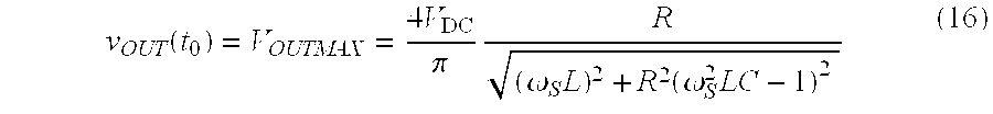
In FIG. 5(b), the fluorescent lamp resistance varies from about 300 Ω to 3 kΩ between lamp power's range—[36 W, 6 W]. In an experiment, the fluorescent lamp may be replaced by a resistor R. Under different VDC, the RMS value of output voltage VOUT is taken and compared with the calculated value (14). The parameters of the prototype are L=360 uH, C=4.7 nF, ωs=(2π) 135 kHz. The resistance equals to 400 Ω, 1 kΩ and 3 kΩ respectively, the absolute error of VOUT is shown in FIG. 6(b), the maximum error is about 2% when VDC changes from 40V to 120V. The high accuracy confirms that the calculation of VOUT(14) is feasible.
As shown in FIG. 7, when t=t0 in one cycle, iC(t0)=0, i.e., V OUT ( 0 ) t = 0 ,
Figure US06580275-20030617-M00010
tan ( ω S t 0 ) = R ( ω S 2 LC - 1 ) ω S L ( 15 )
Figure US06580275-20030617-M00011
Thus, the maximum value of output voltage vOUT(t) happens at t=t0, v OUT ( t 0 ) = V OUTMAX = 4 V DC π R ( ω S L ) 2 + R 2 ( ω S 2 LC - 1 ) 2 ( 16 )
Figure US06580275-20030617-M00012
and the maximum value of iR(t) is I RMAX = V OUTMAX R = 4 V DC π 1 ( ω S L ) 2 + R 2 ( ω S 2 LC - 1 ) 2 ( 17 )
Figure US06580275-20030617-M00013
Based on (4), at t=t0,
V DC =v L(t 0)+v OUT(t 0)
v L(t 0)=−V DC −v OUT(t 0)=−V DC −V OUTMAX =−V LMAX
Then the maximum value of inductor voltage vL(t) is V LMAX = V DC + V OUTMAX = V DC [ 1 + 4 π R ( ω S L ) 2 + R 2 ( ω S 2 LC - 1 ) 2 ] ( 18 )
Figure US06580275-20030617-M00014
The RMS value of iR(t) is I R = V OUT R = 4 V DC 2 π = 1 ( ω S L ) 2 + R 2 ( ω S 2 L ω S C - 1 ) 2 ( 19 )
Figure US06580275-20030617-M00015
Comparing (17) and (19),
I RMAX={square root over (2)}I R  (20)
i L ( t 0 ) = i C ( t 0 ) + i R ( t 0 ) = i R ( t 0 ) = v OUT ( t 0 ) R = I RMAX ( 21 )
Figure US06580275-20030617-M00016
FIG. 8 shows the relationship between IR and VLMAX under different R when VDC changes from 40V to 120V. Different R has its unique slope of IR and VLMAX, the slope stands for the value of resistance indirectly.
The slope of IR and VLMAX can be expressed as K ( R ) = V LMAX I R ( 22 )
Figure US06580275-20030617-M00017
By substituting (18) and (19) into (22), K ( R ) = 2 4 π ( ω S L ) 2 + R 2 ( ω S 2 LC - 1 ) 2 + 2 R ( 23 )
Figure US06580275-20030617-M00018
The relationship of K(R) and R in the prototype is shown in FIG. 9.
The resistance equation can be expressed as R = aK + b = a V LMAX I R + b ( 24 )
Figure US06580275-20030617-M00019
The output power can be defined by
P=V R I R =I 2 R R  (25)
Put (24) into (25),
P=I R(aV LMAX +bI R)  (26)
Based on equation (18), the DC link voltage VDC equals to
V DC =V LMAX −I RMAX R=(1−{square root over (2)}a)V LMAX−{square root over (2)}bI R  (27)
The on-line lamp characteristic can be defined by (24), (26) and (27) after obtaining VLMAX and IR. VLMAX can be achieved from vL(t) by a peak detector easily, and IR can be achieved from vL(t) too, because based on (20) and (21), I R = 2 2 I RMAX = 2 2 i L ( t 0 ) ( 28 )
Figure US06580275-20030617-M00020
It will be seen from the above that simply by using a single sensor to sense inductor voltage vL or inductor current iL, the on-line lamp characteristic can be obtained.
The single-sensor principle can be implemented either using a voltage or a current sensor as shown in FIG. 10. In FIG. 10(a), an extra coupled winding on the inductor is used as a voltage sensor for sensing the inductor voltage vL. In FIG. 10(b), a current sensor (e.g. Hall-effect current sensor) is used to get inductor current iL.
In one embodiment of the invention, the single-sensor principle is demonstrated by the single voltage sensor approach.
Referring to FIG. 10(a), the scale-down inductor voltage vL(t) can be obtained by an extra coupled winding on the inductor. The estimated maximum inductor voltage (i.e., VLMAX) can be obtained by a peak detector. The scale-down inductor current iL(t) can be obtained by integrating vL(t). Comparing the differentiated vL(t) with zero, the moment of ic(t)=0(i.e., t0) can be achieved, because 0.
v L(t)=v s(t)−v out(t) v L ( t ) = v S ( t ) - v OUT ( t ) v L ( t ) t = v S ( t ) t - v OUT ( t ) t v L ( t ) t t = l 0 = 0 ( 29 )
Figure US06580275-20030617-M00021
Because when t=t0, v OUT ( t ) t = 0 , v S ( t ) t = 0.
Figure US06580275-20030617-M00022
Based on (26), the estimated output current IR can be obtained by sampling and holding iL(t) at t0. Therefore, not only the resistance but also the output power and DC link voltage can be estimated at the same time by estimating the inductor voltage.
In FIG. 10(b), a current transducer is used to obtain the scale-down inductor current iL(t). vL(t) comes from differentiating iL(t), VLMAX and IR can be obtained by the similar technique in FIG. 9(a).
FIGS. 11(a)-(c) show the measured and estimated values of the dc link voltage VDC, lamp resistance Rlamp and lamp power Plamp, respectively. The dotted lines represent the measurements and the solid lines represent the estimations using the single voltage sensor approach as shown in FIG. 9(a). The estimations are found to be consistant with measurements.
The present invention has been illustrated above by means of an example in the form of a fluorescent discharge lamp. However, the present invention is also applicable to other forms of discharge lamps such as high intensity discharge (HID) lamps. Indeed the present invention may be particularly useful in the context of HID lamps because they can suffer from are vibration problems. By monitoring the load resistance using an embodiment of the invention the stability of such an HID lamp may be monitored and controlled.

Claims (22)

What is claimed is:
1. Apparatus for determining characteristic(s) of a discharge lamp operated by a high-frequency electronic ballast including a resonant tank comprising an inductor and a capacitor, wherein said characteristic(s) are selected from the group consisting of lamp input voltage, lamp resistance and lamp power, comprising a single sensor for measuring the inductor voltage and/or current, and means for determining said characteristic(s) from the measured inductor voltage and/or current obtained by said single sensor and not other direct measurement.
2. Apparatus as claimed in claim 1 comprising means for obtaining the lamp current and the maximum inductor voltage from the measured inductor voltage and/or current, and wherein said characteristic(s) determining means determines said characteristics from said lamp current and maximum inductor voltage.
3. Apparatus as claimed in claim 1 wherein said characteristic determining means implements the equations: R = aK + b = a V LMAX I R + b
Figure US06580275-20030617-M00023
where R is the lamp resistance, VLMAX is the maximum inductor voltage, IR is the lamp current and a,b are constants;
P=IR(aVLMAX+bIR) where P is lamp power; and
VDC=VLMAX−IRMAXR=(1−{square root over (2)}a)VLMAX−{square root over (2)}bIR where VDC is the input voltage.
4. Apparatus as claimed in claim 3 wherein said apparatus comprises a sensor for measuring the inductor voltage, means for differentiating the inductor voltage to obtain a capacitor current, means for integrating the inductor voltage to obtain an inductor current, means for obtaining the lamp current from the capacitor current and the inductor current, and peak detector means for detecting the maximum inductor voltage.
5. Apparatus as claimed in claim 4 wherein said sensor comprises an extra coupled winding on the inductor.
6. Apparatus as claimed in claim 3 wherein said apparatus comprises a sensor for measuring inductor current, means for differentiating the inductor current to obtain an inductor voltage, means for differentiating the inductor voltage to obtain a capacitor current, means for obtaining the lamp current from the capacitor current and the inductor current, and peak detector means for detecting the maximum inductor voltage.
7. Apparatus as claimed in claim 3 wherein said sensor comprises a Hall-effect current sensor.
8. Apparatus for determining the lamp power, lamp resistance and input voltage of a discharge lamp driven by a power converter circuit including an inductor, comprising a single sensor for measuring the inductor voltage or inductor current, and means for determining the lamp power, lamp resistance and/or input voltage from said measured inductor voltage or inductor current obtained by said single sensor and no other direct measurement.
9. A method for determining the characteristic(s) of a discharge lamp operated by a high-frequency electronic ballast including a resonant tank comprising an inductor and a capacitor, wherein said characteristic(s) are selected from the group consisting of lamp input voltage, lamp resistance and lamp power, comprising measuring the inductor voltage and/or inductor current using a single sensor, and determining said characteristic(s) from the measured inductor voltage and/or current obtained by said single sensor and no other direct measurement.
10. A method as claimed in claim 9 wherein the lamp current and the maximum inductor voltage are obtained from the measured inductor voltage and/or current, and wherein said characteristic(s) is/are determined from said lamp current and maximum inductor voltage.
11. A method as claimed in claim 9 wherein said characteristic(s) is/are determined from the equations: R = aK + b = a V LMAX I R + b
Figure US06580275-20030617-M00024
where R is the lamp resistance, VLMAX is the maximum inductor voltage, IR is the lamp current and a,b are constants;
P=IR(aVLMAX+bIR) where P is lamp power; and
VDC=VLMAX−IRMAXR=(1−{square root over (2)}a)VLMAX−{square root over (2)}bIR where VDC is the input voltage.
12. A method as claimed in claim 11 comprising measuring the inductor voltage, differentiating the inductor voltage to obtain a capacitor current, integrating the inductor voltage to obtain an inductor current, obtaining the lamp current from the capacitor current and the inductor current, and detecting the maximum inductor voltage.
13. A method as claimed in claim 11 comprising measuring the inductor current, differentiating the inductor current to obtain an inductor voltage, differentiating the inductor voltage to obtain a capacitor current, obtaining the lamp current from the capacitor current and the inductor current, and detecting the maximum inductor voltage.
14. A method for determining the lamp power, lamp resistance and input voltage of a discharge lamp driven by a power converter circuit including an inductor, comprising measuring the inductor voltage or inductor current only, and determining the lamp power, lamp resistance and/or input voltage from said measured inductor voltage or inductor current and no other direct measurements.
15. Apparatus for determining the input and/or output voltage of a power electronics converter circuit including an inductor, comprising a single sensor for sensing the voltage across said inductor, and means for calculating the input and output voltage from said inductor voltage only and no other direct measurements.
16. Apparatus as claimed in claim 15 comprising means for integrating the inductor voltage to obtain an inductor current.
17. Apparatus as claimed in claim 16 comprising means for obtaining a load resistance from the inductor current and the output voltage.
18. A method for determining the input and/or output voltage of a power electronics converter circuit including an inductor, comprising sensing only the voltage across said inductor, and calculating the input and output voltage from said inductor voltage only and no other direct measurements.
19. A method as claimed in claim 18 comprising integrating the inductor voltage to obtain an inductor current.
20. A method as claimed in claim 19 comprising obtaining a load resistance from the inductor current and the output voltage.
21. A method of monitoring the load resistance of a discharge lamp driven by a power electronics converter circuit including an inductor, comprising sensing either an inductor current or inductor voltage only and deriving the load resistance from a measurement of the inductor voltage or inductor current from said sensing step and no other direct measurement.
22. Apparatus for monitoring the load resistance of a discharge lamp driven by a power electronics converter circuit including an inductor, comprising a single sensor for measuring an inductor current or inductor voltage, and means for deriving the load resistance from the measured inductor voltage or inductor current obtained by said single sensor and no other direct measurement.
US09/870,408 2000-05-31 2001-05-30 Single sensor control of power converters Expired - Lifetime US6580275B2 (en)

Priority Applications (1)

Application Number Priority Date Filing Date Title
US09/870,408 US6580275B2 (en) 2000-05-31 2001-05-30 Single sensor control of power converters

Applications Claiming Priority (2)

Application Number Priority Date Filing Date Title
US20834300P 2000-05-31 2000-05-31
US09/870,408 US6580275B2 (en) 2000-05-31 2001-05-30 Single sensor control of power converters

Publications (2)

Publication Number Publication Date
US20020030493A1 US20020030493A1 (en) 2002-03-14
US6580275B2 true US6580275B2 (en) 2003-06-17

Family

ID=26903117

Family Applications (1)

Application Number Title Priority Date Filing Date
US09/870,408 Expired - Lifetime US6580275B2 (en) 2000-05-31 2001-05-30 Single sensor control of power converters

Country Status (1)

Country Link
US (1) US6580275B2 (en)

Cited By (6)

* Cited by examiner, † Cited by third party
Publication number Priority date Publication date Assignee Title
US20080265808A1 (en) * 2004-07-10 2008-10-30 Malcolm Eric Sparey Motor Drive Voltage-Boost Control
WO2009129581A1 (en) * 2008-04-24 2009-10-29 Indice Pty Ltd Power control
US20110187287A1 (en) * 2010-02-01 2011-08-04 Empower Electronics, Inc. Ballast configured to compensate for lamp characteristic changes
CN103163439A (en) * 2013-03-16 2013-06-19 南安市柳城高捷图文设计工作室 Method for using and operating comprehensive detector for high intensity discharge (HID) xenon lamp
CN103163440A (en) * 2013-03-16 2013-06-19 南安市柳城高捷图文设计工作室 HID xenon lamp comprehensive detector
CN105699870A (en) * 2016-03-24 2016-06-22 佛山市云米电器科技有限公司 Service life detection apparatus of UV lamp and detection method thereof

Families Citing this family (2)

* Cited by examiner, † Cited by third party
Publication number Priority date Publication date Assignee Title
CN103235248B (en) * 2013-03-16 2015-01-21 南安市柳城高捷图文设计工作室 Maintenance method of HID (high intensity discharge) ballast
US9812968B2 (en) * 2014-11-19 2017-11-07 Futurewei Technologies, Inc. Zero voltage switching detection apparatus and method

Citations (6)

* Cited by examiner, † Cited by third party
Publication number Priority date Publication date Assignee Title
US4288739A (en) * 1980-03-10 1981-09-08 Kepco, Inc. Dynamic load for testing regulated power supplies
US4346332A (en) * 1980-08-14 1982-08-24 General Electric Company Frequency shift inverter for variable power control
US4810950A (en) * 1986-07-17 1989-03-07 Ob Products, Inc. Load resistance measuring technique
US4866367A (en) * 1988-04-11 1989-09-12 Virginia Tech Intellectual Properties, Inc. Multi-loop control for quasi-resonant converters
US5475296A (en) 1994-04-15 1995-12-12 Adept Power Systems, Inc. Digitally controlled switchmode power supply
US5602463A (en) 1995-12-11 1997-02-11 Lockheed Martin Corporation DC power supply with enhanced input power factor using a buck and boost converter

Patent Citations (6)

* Cited by examiner, † Cited by third party
Publication number Priority date Publication date Assignee Title
US4288739A (en) * 1980-03-10 1981-09-08 Kepco, Inc. Dynamic load for testing regulated power supplies
US4346332A (en) * 1980-08-14 1982-08-24 General Electric Company Frequency shift inverter for variable power control
US4810950A (en) * 1986-07-17 1989-03-07 Ob Products, Inc. Load resistance measuring technique
US4866367A (en) * 1988-04-11 1989-09-12 Virginia Tech Intellectual Properties, Inc. Multi-loop control for quasi-resonant converters
US5475296A (en) 1994-04-15 1995-12-12 Adept Power Systems, Inc. Digitally controlled switchmode power supply
US5602463A (en) 1995-12-11 1997-02-11 Lockheed Martin Corporation DC power supply with enhanced input power factor using a buck and boost converter

Non-Patent Citations (1)

* Cited by examiner, † Cited by third party
Title
Ohnuki et al., "Control of a Three-Phase PWM Rectifier Using Estimated AC-Side and DC-Side Voltages," IBEE Transactions on Power Electronics, vol. 14, No. 2, (Mar. 1999).

Cited By (12)

* Cited by examiner, † Cited by third party
Publication number Priority date Publication date Assignee Title
US20080265808A1 (en) * 2004-07-10 2008-10-30 Malcolm Eric Sparey Motor Drive Voltage-Boost Control
US8004220B2 (en) * 2004-07-10 2011-08-23 Trw Limited Motor drive voltage-boost control
WO2009129581A1 (en) * 2008-04-24 2009-10-29 Indice Pty Ltd Power control
US20110043112A1 (en) * 2008-04-24 2011-02-24 Indice Pty Ltd Power control
US8476841B2 (en) 2008-04-24 2013-07-02 Indice Pty Ltd Power control
US20110187287A1 (en) * 2010-02-01 2011-08-04 Empower Electronics, Inc. Ballast configured to compensate for lamp characteristic changes
US8773037B2 (en) 2010-02-01 2014-07-08 Empower Electronics, Inc. Ballast configured to compensate for lamp characteristic changes
CN103163439A (en) * 2013-03-16 2013-06-19 南安市柳城高捷图文设计工作室 Method for using and operating comprehensive detector for high intensity discharge (HID) xenon lamp
CN103163440A (en) * 2013-03-16 2013-06-19 南安市柳城高捷图文设计工作室 HID xenon lamp comprehensive detector
CN103163440B (en) * 2013-03-16 2015-01-07 南安市柳城高捷图文设计工作室 HID xenon lamp comprehensive detector
CN103163439B (en) * 2013-03-16 2015-04-01 南安市柳城高捷图文设计工作室 Method for using and operating comprehensive detector for high intensity discharge (HID) xenon lamp
CN105699870A (en) * 2016-03-24 2016-06-22 佛山市云米电器科技有限公司 Service life detection apparatus of UV lamp and detection method thereof

Also Published As

Publication number Publication date
US20020030493A1 (en) 2002-03-14

Similar Documents

Publication Publication Date Title
US6297621B1 (en) Voltage sensorless control of power converters
US6016257A (en) Voltage regulated power supply utilizing phase shift control
EP0893039B1 (en) Ballast circuit
DE60101978T2 (en) Dimmable ECG
US8044643B1 (en) Power supply switching circuit for a halogen lamp
US5614810A (en) Power factor correction circuit
CN110048597B (en) Control method, controller and system of power factor correction circuit
EP0350104B1 (en) A signal generating circuit for ballast control of discharge lamps
EP0649271A1 (en) Metal halide electronic ballast
US8199534B2 (en) Load current detection in electrical power converters
US20040012985A1 (en) Resonant converter with phase delay control
Pottker et al. Power factor correction of non-linear loads employing a single phase active power filter: control strategy, design methodology and experimentation
US6580275B2 (en) Single sensor control of power converters
EP0622888B1 (en) Improved power factor DC power supply
US7750577B2 (en) Apparatus and method for providing an isolated set point from an input signal applied to a lamp ballast
JP7293968B2 (en) CONTROL CIRCUIT FOR POWER CONVERTER AND POWER CONVERTER
US20220399808A1 (en) Control circuit and ac-dc power supply applying the same
EP0765632A2 (en) Method and apparatus for respiration monitoring
US7557513B2 (en) Discharge lamp lighting circuit
TW200418347A (en) Device and method for determining the current flowing through a gas discharge lamp
RU2326484C1 (en) Semi-bridge transistor inverter
KR100735270B1 (en) Piezoelectric transformer driving apparatus
JP2882060B2 (en) Method for detecting idle operation of inverter for induction heating
CN116979715A (en) Inductance current time domain model online modeling method and device for SS type WPT system
JP3043947B2 (en) Power supply circuit

Legal Events

Date Code Title Description
AS Assignment

Owner name: CITY UNIVERSITY OF HONG KONG, HONG KONG

Free format text: ASSIGNMENT OF ASSIGNORS INTEREST;ASSIGNORS:HUI, SHU-YUEN RON;CHUNG, SHU-HUNG HENRY;REEL/FRAME:012126/0056

Effective date: 20010712

STCF Information on status: patent grant

Free format text: PATENTED CASE

FPAY Fee payment

Year of fee payment: 4

FPAY Fee payment

Year of fee payment: 8

FEPP Fee payment procedure

Free format text: PAYOR NUMBER ASSIGNED (ORIGINAL EVENT CODE: ASPN); ENTITY STATUS OF PATENT OWNER: LARGE ENTITY

FEPP Fee payment procedure

Free format text: PAT HOLDER NO LONGER CLAIMS SMALL ENTITY STATUS, ENTITY STATUS SET TO UNDISCOUNTED (ORIGINAL EVENT CODE: STOL); ENTITY STATUS OF PATENT OWNER: LARGE ENTITY

REFU Refund

Free format text: REFUND - PAYMENT OF MAINTENANCE FEE, 12TH YR, SMALL ENTITY (ORIGINAL EVENT CODE: R2553); ENTITY STATUS OF PATENT OWNER: LARGE ENTITY

FPAY Fee payment

Year of fee payment: 12