US6563177B2 - Semiconductor memory device having a trench and a gate electrode vertically formed on a wall of the trench - Google Patents
Semiconductor memory device having a trench and a gate electrode vertically formed on a wall of the trench Download PDFInfo
- Publication number
- US6563177B2 US6563177B2 US09/120,116 US12011698A US6563177B2 US 6563177 B2 US6563177 B2 US 6563177B2 US 12011698 A US12011698 A US 12011698A US 6563177 B2 US6563177 B2 US 6563177B2
- Authority
- US
- United States
- Prior art keywords
- transistor
- gate electrode
- wall
- load
- trench
- Prior art date
- Legal status (The legal status is an assumption and is not a legal conclusion. Google has not performed a legal analysis and makes no representation as to the accuracy of the status listed.)
- Expired - Lifetime
Links
Images


Classifications
-
- H—ELECTRICITY
- H10—SEMICONDUCTOR DEVICES; ELECTRIC SOLID-STATE DEVICES NOT OTHERWISE PROVIDED FOR
- H10B—ELECTRONIC MEMORY DEVICES
- H10B10/00—Static random access memory [SRAM] devices
-
- G—PHYSICS
- G11—INFORMATION STORAGE
- G11C—STATIC STORES
- G11C11/00—Digital stores characterised by the use of particular electric or magnetic storage elements; Storage elements therefor
- G11C11/21—Digital stores characterised by the use of particular electric or magnetic storage elements; Storage elements therefor using electric elements
- G11C11/34—Digital stores characterised by the use of particular electric or magnetic storage elements; Storage elements therefor using electric elements using semiconductor devices
- G11C11/40—Digital stores characterised by the use of particular electric or magnetic storage elements; Storage elements therefor using electric elements using semiconductor devices using transistors
- G11C11/41—Digital stores characterised by the use of particular electric or magnetic storage elements; Storage elements therefor using electric elements using semiconductor devices using transistors forming static cells with positive feedback, i.e. cells not needing refreshing or charge regeneration, e.g. bistable multivibrator or Schmitt trigger
- G11C11/412—Digital stores characterised by the use of particular electric or magnetic storage elements; Storage elements therefor using electric elements using semiconductor devices using transistors forming static cells with positive feedback, i.e. cells not needing refreshing or charge regeneration, e.g. bistable multivibrator or Schmitt trigger using field-effect transistors only
-
- H—ELECTRICITY
- H10—SEMICONDUCTOR DEVICES; ELECTRIC SOLID-STATE DEVICES NOT OTHERWISE PROVIDED FOR
- H10B—ELECTRONIC MEMORY DEVICES
- H10B10/00—Static random access memory [SRAM] devices
- H10B10/15—Static random access memory [SRAM] devices comprising a resistor load element
-
- Y—GENERAL TAGGING OF NEW TECHNOLOGICAL DEVELOPMENTS; GENERAL TAGGING OF CROSS-SECTIONAL TECHNOLOGIES SPANNING OVER SEVERAL SECTIONS OF THE IPC; TECHNICAL SUBJECTS COVERED BY FORMER USPC CROSS-REFERENCE ART COLLECTIONS [XRACs] AND DIGESTS
- Y10—TECHNICAL SUBJECTS COVERED BY FORMER USPC
- Y10S—TECHNICAL SUBJECTS COVERED BY FORMER USPC CROSS-REFERENCE ART COLLECTIONS [XRACs] AND DIGESTS
- Y10S257/00—Active solid-state devices, e.g. transistors, solid-state diodes
- Y10S257/903—FET configuration adapted for use as static memory cell
- Y10S257/904—FET configuration adapted for use as static memory cell with passive components,, e.g. polysilicon resistors
Definitions
- the present invention relates to a semiconductor memory device and fabrication method thereof.
- An SRAM(Static Random Access Memory) cell also referred to as a flip-flop, is composed of a pair of cross-coupled inverters. That is, the memory cell's logic state is determined by a voltage level of each a pair of inverter output nodes, and when an inverter output node to which a supply voltage is applied is at a low voltage level, the other inverter output node maintains a high voltage level. Once the memory cell becomes stabilized, the stable state is maintained, so that a SRAM cell does not require a periodic refresh operation for having data stored therein, and such a characteristic of the SRAM cell is distinguishable from a DRAM (Dynamic Random Access Memory) cell.
- DRAM Dynamic Random Access Memory
- an SRAM cell is more stably operated than a DRAM cell, with a less power consumption. Also, due to self-restoring, peripheral circuits characteristics, the SRAM cell is operated in a faster mode, compared to other kinds of semiconductor memory cells.
- the SRAM cell requires at least 6 transistors for forming a single cell of the kind and accordingly exhibits a lower integration factor.
- a six-transistor TFT (Thin Film Transistor) SRAM cell is widely adopted mainly due to a cell data retention stability and reduced current consumption, even though the TFT SRAM cell is composed of a six-transistor set, and further TFT SRAM cell occupies a larger region than a high-resistance load SRAM cell which employs a polysilicon resistor.
- TFT Thin Film Transistor
- an equivalent circuit of a conventional SRAM cell is provided with a pair of NMOS access transistors Ta 1 , Ta 2 , a pair of NMOS drive transistors Td 1 , Td 2 , and a pair of PMOS load transistors Tl 1 , Tl 2 , wherein the access transistors Ta 1 , Ta 2 will be referred to as a first and second access transistors, the drive transistors Td 1 , Td 2 will be respectively referred to as the first and second drive transistors, and the load transistors Tl 1 , Tl 2 will be respectively referred to as first and second load transistors or first and second load resistors.
- the gates of the first and second access transistors Ta 1 , Ta 2 are respectively connected to a word line.
- One end of the channel of the first access transistor Ta 1 is connected to a bit line BL, and node A connected to the other end of the channel of the first access transistor Ta 1 is connected in common to the gate of the second load transistor Tl 2 and the gate of the second drive transistor Td 2 .
- One end of the channel of the second access transistor Ta 2 is connected to a complementary bar bit line /BL, and node B of the second access transistor Ta 2 is connected in common to the gate of the first load transistor Tl 1 and the gate of the first drive transistor Td 1 .
- each of the first and second load transistors Tl 1 , Tl 2 is connected in common to high level supply voltage Vdd, and the source region of each of the first and second drive transistors Td 1 , Td 2 is connected in common to ground voltage Vss.
- the voltage at node B becomes practically 0V, so that the first load transistor Tl 1 becomes turned on and the first drive transistor Td 1 is turned off, whereby data “1” is transferred to the SRAM cell. So long as current is continuously supplied after a data voltage of the SRAM cell is determined, the first load transistor Tl 1 remains turned on so that the supply voltage Vdd is applied via the first load transistor Tl 1 to the node A, and the second drive transistor Td 2 remains turned on so that the current of node B flows through the second drive transistor Td 2 to ground Vss, whereby node A is turned to a high level and node B is turned to a low level so as to maintain the stored data.
- the steps contrary to those for a data “1” are taken for a data “0”. That is, the low-level voltage Vss is applied to the bit line BL, and the high level voltage Vdd is applied to the bar bit line /BL, so that the node A maintains a low level and the node B maintains a high level
- bit line pair BL, /BL for reading data are set at about 3V which is an operation point of a sense amplifier in order equalize the bit line pair BL, /BL with regard to voltage.
- the word line voltage is raised to the level of supply voltage Vdd, and the first and second access transistors Ta 1 , Ta 2 are turned on so as to select the target SRAM cell for carrying out a reading operation.
- the voltage of the bit line BL is slightly raised toward the level of Vdd due to the current which flows in through the first load transistor Tl 1 , and the voltage of the bar bit line /BL flows to ground Vss and is slightly lowered, accordingly.
- the potential difference between the bit line BL and the bar bit line /BL is amplified in the sense amplifier (not shown) and transferred to an output buffer (not shown).
- the reading of the data “0” follows steps identical to those for a data “1”, wherein the voltage fluctuation of the bit line BL and the bar bit line /BL is reversed compared to the case of a data “1”.
- the first and second drive transistors Td 1 , Td 2 and the first and second access transistors Ta 1 , Ta 2 are respectively formed of a bulk transistor, and because the first and second load transistors Tl 1 , Tl 2 are respectively provided with a structure in which the transistors Tl 1 , Tl 2 are sequentially stacked on the first and second drive transistors Td 1 , Td 2 , the TFT SRAM becomes advantageous in that it requires less chip region than a general SRAM.
- FIG. 2 illustrating a plan layout view of a conventional TFT SRAM and to FIGS. 3A-3G showing fabrication sequence cross-sectional views thereof, the structure of the TFT SRAM will now be described.
- a device isolation region 2 a On the region of the substrate 1 other than the device isolation region 2 a are formed the first and second access transistors Ta 1 , Ta 2 and the first and second drive transistors Td 1 , Td 2 . That is, on the semiconductor substrate 1 are respectively formed gate electrodes 5 a 1 , 5 a 2 of the first and second access transistors Ta 1 , Ta 2 .
- Gate electrodes 5 d 1 , 5 d 2 of the first and second drive transistors Td 1 , Td 2 are formed on the semiconductor substrate 1 .
- Td 2 On the semiconductor substrate 1 and adjacent to sides of the gate electrodes 5 d 1 , 5 d 2 of the first and second drive transistors Td 2 , Td 2 are formed source regions 3 d 1 , 3 d 2 and drain regions 4 d 1 , 4 d 2 of the first and second drive transistors Td 1 , Td 2 , wherein the first drive transistor Td 1 includes the gate electrode 5 d 1 , source region 3 d 1 , and drain region 4 d 1 , and the second drive transistor Td 2 is provided with gate electrode 5 d 2 , source region 3 d 2 and drain region 4 d 2 .
- the drain region 4 a 1 of the first access transistor Ta 1 is connected by a butting contact to the gate electrode 5 d 2 of the second drive transistor Td 2 .
- the drain region 4 a 2 of the second access transistor Ta 2 is connected by a butting contact to the gate electrode 5 a 1 of the first drive transistor Td 1 , but the respective contact regions thereof are not shown in the drawings.
- a gate electrode 7 l 1 of the first load transistor Tl 1 and a gate electrode 7 l 2 of the second load transistor Tl 2 are formed on the first and second drive transistors Td 1 , Td 2 .
- An active layer 9 of the first and second load transistors is formed on the gate electrodes 7 l 1 , 7 l 2 of the first and second load transistors Tl 1 , Tl 2 .
- In the active layer 9 are formed source region regions 10 l 1 , 10 l 2 and drain regions 11 l 1 , 11 l 2 of the first and second load transistors Tl 1 , Tl 2 .
- the source region regions 10 l 1 , 10 l 2 of the first and second load transistors Tl 1 , Tl 2 are respectively connected to a Vdd line.
- the node A as shown in FIG. 1 denoting a contact point between the drain region 3 d 1 of the first drive transistor Td 1 and the drain 11 l 1 of the first load transistor Tl 1 is connected through a first contact hole CT 1 and a second contact hole CT 2 to the gate electrode 5 d 2 of the second drive transistor Td 2 and the gate electrode 7 l 2 of the second load transistor Tl 2 .
- FIGS. 3A through 3G illustrating cross-sectional process views taken along line III—III in FIG. 2, the fabrication process thusly constituted conventional stack type TFT SRAM cell will now be described.
- a p-type semiconductor substrate 1 there are formed device isolation regions 2 a and active regions 2 b respectively of a gate oxide film 41 , wherein the device isolation regions 2 a are formed using a LOCOS (LOCal Oxidation on Silicon) method.
- LOCOS LOCal Oxidation on Silicon
- a polysilicon layer which is then patterned for thereby forming the gate electrodes 5 a 1 , 5 a 2 of the first and second access transistors Ta 1 , Ta 2 .
- n-type impurities are ion-implanted into portions of the substrate 1 adjacent to each side of the gate electrode 5 a 1 , 5 a 2 for thereby forming source regions 3 a 1 , 3 a 2 and drains 4 a 1 , 4 a 2 of the first and second access transistors Ta 1 , Ta 2 .
- a photoresist film 42 is formed on the gate oxide film 41 including the patterned gate electrodes 5 a 1 , 5 a 2 and patterned so as for predetermined portions of the drains 4 a 1 , 4 a 2 of the first and second access transistors Ta 1 , Ta 2 to be exposed therethrough using a photo lithographic method.
- the gate oxide film 41 portions which are on the substrate 1 portion beneath which are formed the drains 4 a 1 , 4 a 2 of the first and second access transistors Ta 1 , Ta 2 are moved.
- the gate oxide film 41 is so thin that it is significantly difficult to etchingly remove the gate oxide film 41 without damaging the adjacent drain regions 4 a 1 , 4 a 2 and causing defects in the first and second access transistors Ta 1 , Ta 2 .
- FIG. 3 B After removing the remaining photoresist film 42 , another photoresist film (not shown) is formed instead on the remaining patterns as shown in FIG. 3 B.
- the photo resist film (not shown) portions are formed on regions for forming the drive transistors Td 1 , Td 2 , and a polysilicon layer is patterned to form the gate electrodes 5 d 1 , 5 d 2 of the drive transistors Td 1 , Td 2 .
- a polysilicon layer is selectively deposited for thereby forming the gate electrodes 5 d 1 , 5 d 2 of the drive transistors Td 1 , Td 2 as shown in FIG. 3 C.
- FIG. 3C for convenience' sake, the gate electrode 5 d 2 of the second drive transistor Td 2 is illustrated but the gate electrode 5 d 1 of the first drive transistor Td 1 is not illustrated in FIG. 3 C.
- Impurities are ion-implanted into the semiconductor substrate 1 adjacent to the sides of the gate electrodes 5 d 1 , 5 d 2 of the first and second drive transistors Td 1 , Td 2 so as to form source regions (not shown) and drain regions (not shown) of the drive transistors Td 1 , Td 2 .
- the remaining photoresist film 42 ′ is then removed.
- an SiO2 film serving as a first insulation film 6 is formed with a thickness of 50 100 nm over the thusly formed structure including the gate electrodes 5 d 1 , 5 d 2 of the first and second drive transistors Td 1 , Td 2 by using a CVD (Chemical Vapor Deposition) process.
- the contact hole CT 3 is formed in a predetermined portion of the gate electrode 5 d 2 of the second drive transistor Td 2
- the contact hole CT 1 is formed in a predetermined portion of the gate electrode 5 d 1 of the first drive transistor Td 1 .
- a polysilicon layer is formed on the CVD SiO2 film serving as the first insulation film 6 and in the contact holes CT 1 , CT 3 using a LPCVD (Low Pressure Chemical Vapor Deposition) process at a temperature of 630(C.
- LPCVD Low Pressure Chemical Vapor Deposition
- phosphorous impurities are ion-implanted through the poly silicon layer which is then patterned to thereby form gate electrodes 7 l 1 , 7 l 2 of the first and second load transistors Tl 1 , Tl 2 .
- a gate oxide film serving as a second insulation film 8 is formed on the gate electrodes 7 l 1 , 7 l 2 of the first and second load transistors Tl 1 , Tl 2 and the first insulation film, wherein the gate oxide film can be one selected from an SiO2 film using the LPCVD process, a multi-layer film of SiO2/Si3N4, and a TESO film.
- the contact hole CT 4 for being connected to the drain 11 l 1 of the first load transistor Tl 1
- the contact hole CT 2 for being connected to the drain region 11 l 2 of the second load transistor Tl 2 .
- an amorphous silicon layer 9 is formed on the second insulation film 8 and in the contact holes CT 2 , CT 4 with a thickness of less than 40 nm at a temperature of 520 C. by a LPCVD process and patterned.
- the amorphous silicon layer 9 is annealed at a low temperature in order to be polycrystallized, that is, to be polysiliconized.
- the low temperature annealing is applied to increase the grains of the polysilicon layer in size; the larger the grains, the better becomes an on/off current characteristic of a transistor.
- the multi-crystallized polysilicon layer 9 is provided to be used for an active layer and a Vdd line of the first and second load transistors Tl 1 , Tl 2 .
- a photoresist film is deposited on the active layer 9 and the Vdd line 9 of the first and second load transistors Tl 1 , Tl 2 and patterned by applying an etching so as for only a photo resist film pattern 43 a to remain on a channel formation region.
- BF2 is ion-implanted with an energy of 25 KeV at a 2-4*1014/cm2 dose, for thereby forming source regions 10 l 1 , 10 l 2 and drain regions 11 l 1 , 11 l 2 of the first and second load transistors and a Vdd line.
- the semiconductor memory device includes a trench formed in a semiconductor substrate and having at least two walls including a first wall and a second wall, and the first drive transistor and the second drive transistor including a source region and a drain region respectively formed at the first wall and the second wall of the trench, and a gate electrode respectively formed on the first wall and the second wall of the trench.
- the semiconductor memory device includes a trench formed in a semiconductor substrate and having at least two walls including a first wall and a second wall, and the first access transistor and the second transistor respectively including a respective gate electrode formed at the first and the second walls of the trench, and a source region and a drain region respectively formed at the each side of the corresponding gate electrode in the semiconductor substrate.
- the semiconductor memory device comprises a semiconductor substrate, a trench formed in the semiconductor substrate and having at least four walls including a first wall, a third wall and a fourth wall, wherein the first drive transistor and the second drive transistor each including a source region, a drain region and a gate electrode are formed at the first wall and the third wall of the trench, respectively, the first access transistor and the second access transistor each including a source region, a drain region and a gate electrode are formed at the second wall the fourth wall of the trench, respectively, and the first load resistor and the
- a semiconductor memory device fabrication method which includes the steps of preparing a semiconductor substrate, forming a plurality of first impurity regions in the semiconductor substrate for serving as source regions and drain regions of a first access transistor, a second access transistor, a first drive transistor and a second drive transistor, forming an insulation layer on the semiconductor substrate, forming a first contact hole in one of the plurality of the first impurity regions serving as the drain region of the first drive transistor, and forming a second contact hole in another first impurity region serving as the drain region of the second drive transistor, forming a conductive layer on the insulation layer and in the first and the second contact holes, forming a plurality of second impurity regions in a portion of the conductive layer for serving as source region and drain region of a first and second load transistor, patterning the conductive layer, for forming a first active layer of the first load transistor and a second active layer of the second load transistor, forming a trench having at least four walls
- a semiconductor memory device fabrication method which includes the steps of preparing a semiconductor substrate, forming a plurality of impurity regions in the semiconductor substrate for serving as source regions and drain regions of a first access transistor, a second access transistor, a first drive transistor and a second drive transistor, forming an insulation layer on the semiconductor substrate, forming a first contact hole in one of the plurality of first impurity regions serving as a drain region of the first drive transistor, and forming a second contact hole in another first impurity region serving as a drain region of the second drive transistor, forming a conductive layer on the insulation layer and in the first and the second contact holes, forming first and second load resistors by patterning the first conductive layer, forming a trench having at least four walls including a fit wall, a second wall, a third wall and a fourth wall, by etching a portion of the semiconductor substrate to a predetermined depth of the semiconductor substrate, wherein the plurality of first impurity
- FIG. 1 is an equivalent circuit view of a conventional TFT SRAM cell
- FIG. 2 is a plan layout view of the conventional TFT SRAM cell
- FIGS. 3A through 3G are cross-sectional process sequence views of the conventional TFT SRAM cell taken along line III—III in FIG. 2;
- FIGS. 4 A through 4 K′ are process views of a TFT SRAM cell according to the present invention.
- FIG. 5 is an equivalent circuit view of an SRAM cell using a load resistor
- FIGS. 6A through 6K are process views of an SRAM cell using a load resistor according to the present invention.
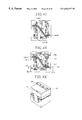
- FIGS. 4 D and 4 D′ respectively illustrating the structure of the SRAM cell according to the present invention
- a trench 2 having four walls, a first wall 2 a , a second wall 2 b , a third wall 2 c and a fourth wall 2 d .
- first wall 2 a and third wall 2 c facing each other, of the four walls 2 a , 2 b , 2 c , 2 d of the trench 2 there are formed a second conductivity type impurity regions serving as source regions ds 1 , ds 2 and drains dd 1 , dd 2 of the first and second drive transistors Td 1 , Td 2 , respectively.
- the semiconductor substrate is formed of a first conductivity type that is opposite to the second conductivity type. Specifically, the source region ds 1 and the drain dd 1 of the first drive transistor Td 1 are formed in the first wall 2 a , and the source region ds 2 and drain dd 2 of the second drive transistor Td 2 are formed in the third wall 2 c . On the upper surface of the semiconductor substrate 1 corresponding to the first wall 2 a there is formed a first active layer 4 a serving as an active layer of the first load transistor Tl 1 . The first active layer 4 a is formed of the second conductivity type.
- a second active layer 4 b serving as an active layer of the second load transistor Tl 2 .
- the second active layer 4 b is also formed of the second conductivity type.
- a plurality of impurity regions of first conductivity type are formed in the first active layer and the second active layer.
- the impurity regions are employed as a source region ls 1 and a drain region ld 1 of the first load transistor Tl 1 and as a source region ls 2 and a drain region ld 2 of the second load transistor Tl 2 .
- a wall of the first active layer 4 a of the first load transistor Tl 1 and the first wall 2 a have a vertically aligned side edge.
- a wall of the second load transistor Tl 2 and the third wall 2 c also have a vertically aligned side edge.
- a first gate oxide film 6 a is formed on the wall of the first active layer 4 a and the first wall 2 a of the trench 2 .
- a second gate oxide film 6 b is formed on a wall of the second active layer 4 b and the third wall 2 c of the trench 2 .
- a first gate electrode 8 a serving as a common gate electrode of the first load transistor Tl 1 and the first drive transistor Td 1 .
- a second gate electrode 8 b serving as a common gate electrode of the second load transistor Tl 2 and the second drive transistor Td 2 . Therefore, the channels of the first and the second drive transistors Td 1 , Td 2 are formed to be perpendicular to the upper surface of the semiconductor substrate 1 and parallel to the surface of the each wall of the trench 2 .
- a source region as 1 and drain region ad 1 of the first access transistor Ta 1 are formed in the second wall 2 b facing the fourth wall 2 d of the four walls 2 a , 2 b , 2 c , 2 d in the trench 2
- a source region as 2 and drain region ad 2 of the second access transistor Ta 2 are formed in a fourth wall 2 d facing the second wall 2 b of the four walls 2 a , 2 b , 2 c , 2 d in the trench 2 .
- a gate oxide film (not shown) for the first and second access transistors Ta 1 , Ta 2 is formed on the second wall 2 b and the fourth wall 2 d , respectively.
- the gate oxide film (not shown) are formed the gate electrodes 12 a , 12 b of the first and second access transistors Ta 1 , Ta 2 .
- a word line WL for connecting the gate electrode 12 a to the gate electrode 12 b .
- the drain region dd 1 of the first drive transistor Td 1 is shared with the drain region ad 1 of the first access transistor Ta 1 .
- drain region dd 2 of the second drive transistor Td 2 is shared with the drain region ad 2 of the second access transistor Ta 2 .
- the common drain region of ad 1 and dd 1 is located in the corner formed by first wall 2 a and second wall 2 b of the trench 2 .
- the common drain region of ad 2 and dd 2 is located in the corner formed by the third wall 2 c and the fourth wall 2 d of the trench 2 .
- a Vdd line 16 is formed over the trench 2 and on an upper surface of an insulation layer formed on the thus far described entire pattern for thereby being connected to the source regions ls 1 , ls 2 of the first and second load transistors Tl 1 , Tl 2 , and as further shown in FIG. 4K, on the so far described pattern there are formed a bit line BL connected to the source region as 1 of the first access transistor Ta 1 and a bar bit line /BL connected to the source region as 2 of the second access transistor Ta 2 .
- FIG. 4A which illustrates a plan view
- FIG. 4 A′ which illustrates a perspective view of a cross-section taken along line IVa′—IVa′ in FIG. 4A
- a plurality of impurity regions as 1 , ad 1 and dd 1 , as 2 , ad 2 and dd 2 , ds 1 and ds 2 are formed in the semiconductor substrate 1 to form source region ds 1 and drain region dd 1 of the first drive transistor Td 1 , source region ds 2 and drain region dd 2 of the second drive transistor Td 2 , source region as 1 and drain region ad 1 of the first access transistor Ta 1 , and source region as 2 and drain region ad 2 of the second access transistor Ta 2 .
- FIG. 4B which illustrates a plan view
- FIG. 4 B′ which illustrates a perspective cross sectional view taken along line IVb′—IVb′ in FIG. 4B
- an insulation film 3 is formed on the upper surface of the substrate 1 .
- a first contact hole Cont 1 for connecting the drain region dd 1 of the first drive transistor Td 1 and the drain region ld 1 of the first load transistor Tl 1
- a second contact hole Cont 2 for connecting the drain region dd 2 of the second drive transistor Td 2 and the drain region ld 2 of the second load transistor Tl 2 .
- an amorphous silicon layer is deposited in the contact holes Cont 1 , Cont 2 and on the insulation layer 3 with a thickness of less than 40 nm, and an annealing is applied thereto at a low temperature so as to change the amorphous silicon layer into polysilicon layer.
- the polysilicon layer is patterned using a photo-lithographic process and an etching process to form the first active layer 4 a serving as an active layer for the first load transistor Tl 1 , and the second active layer 4 b serving as an active layer for the second load transistor Tl 2 .
- FIG. 4C which illustrates a plan view
- FIG. 4 C′ which illustrates a perspective view of a cross-section taken along line IVc′—IVc′ in FIG. 4C
- an ion-implantation is carried out on predetermined portions of the active layers 4 a , 4 b for thereby forming the source regions ls 1 , ls 2 and the drain regions ld 1 , ld 2 of the first and second load transistors Tl 1 , Tl 2 .
- an SOG (Spin On Glass) insulation layer 5 is formed on the active layer 4 of the first and second load transistors Tl 1 , Tl 2 and the insulation layer 3 for thereby planarizing the structure.
- SOG Spin On Glass
- portions of the active layers 4 a , 4 b of the first and second load transistors Tl 1 , Tl 2 , the SOG layer 5 and the insulation layer 3 are anisotropically etched using an RIE (Reactive Ion Etching) process.
- RIE Reactive Ion Etching
- the above-described etching is continuously carried out into the semiconductor substrate 1 for thereby forming the trench 2 having four walls, the first wall 2 a , the second wall 2 b , the third wall 2 c and the fourth wall 2 d .
- the trench 2 is formed to be deeper than the impurity regions as 1 , as 2 , ad 1 , ad 2 , ds 1 , ds 2 , dd 1 , dd 2 .
- the impurity regions as 1 , as 2 , ad 1 , ad 2 , ds 1 , ds 2 , dd 1 and dd 2 are exposed by forming the trench 2 .
- the first gate oxide film 6 a is formed on the first wall 2 a for forming the first drive transistor Td 1 and a wall of the first active layer 4 a serving as an active layer of the first load transistor Tl 1
- the second gate oxide film 6 b is formed on the third wall 2 c for forming the second drive transistor Td 2 and a wall of the second active layer 4 b serving as an active layer of the second load transistor Tl 2
- the first and second gate oxide films can be formed of one selected from SiO2, TESO, and SiO2/SiO3N4.
- a third contact hole Cont 3 is formed in the drain region ld 1 of the first load transistor Tl 1
- a fourth contact hole Cont 4 is formed in the drain region ld 2 of the second load transistor Tl 2 .
- the third contact hole Cont 3 serves to connect in common the second gate electrode 8 b to the second load transistor Tl 2 and the second drive transistor Td 2
- the fourth contact hole Cont 4 serves to connect in common the first gate electrode 8 a to the first load transistor Tl 1 and the first drive transistor Td 1 .
- a polysilicon layer is deposited on the entire upper surface of the structure including the surface of the gate oxide layer 6 a , 6 b and the contact holes Cont 3 , Cont 4 , and patterned to form the first gate electrode 8 a , the second gate electrode 8 b and a polysilicon wire 8 c , so that the first gate electrode 8 a serving as a common gate electrode of the first load transistor Tl 1 and the first drive transistor Td 1 is formed on a side surface of the first gate oxide film 6 a , and the second gate electrode 8 b serving as a common gate electrode of the second load transistor Tl 2 and the second drive transistor Td 2 is formed on a side surface of the second gate oxide film 6 b .
- the second gate electrode 8 b is connected through the third and fourth contact holes Cont 3 , Cont 4 to the drain region dd 1 of the first load transistor Tl 1 , and the polysilicon wire 8 c is formed so as to connect the drain region dd 2 of the second load transistor Tl 2 to the first gate electrode 8 a formed on a wall facing the drain region dd 2 .
- FIGS. 4 G and 4 G′ are a perspective view of a cross-section taken along line IVg′—IVg′ in FIG. 4G
- an oxide films 10 a , 10 b are formed on the second wall 2 b and the fourth wall 2 d of trench 2 .
- a polysilicon layer is deposited on the entire structure and patterned to there by form a gate electrode 12 a , 12 b of the first access transistor Ta 1 and the second access transistor Ta 2 on the side surface of oxide film 10 a , 10 b formed on the second wall 2 b and fourth wall 2 d respectively.
- a word line connecting the gate electrode 12 a and the gate electrode 12 b is formed in the trench 2 .
- FIGS. 4H, 4 I and 4 I′ are a perspective view of a cross-section taken along lines IVi′—IVi′ in FIG. 41, an SOG film 14 is deposited in the trench 2 and on the upper surface of the structure for thereby planarizing the structure.
- an SOG film 14 is deposited in the trench 2 and on the upper surface of the structure for thereby planarizing the structure.
- the source regions ls 1 , ls 2 of the first and second load transistors Tl 1 , Tl 2 there are formed fifth and sixth contact holes Cont 5 , Cont 6 .
- a conductive layer is formed in the contact holes Cont 5 , Cont 6 and on the SOG film 14 , and patterned for thereby forming the Vdd line 16 .
- the conductive layer 16 is formed of one selected from polysilicon, and metals such as aluminum, tungsten and metallic silicide.
- FIGS. 4 K and 4 K′ are a perspective view of a cross-section taken along lines IVk′—IVk′ FIG. 4K an insulation layer 18 is formed on the Vdd line 16 and the SOG layer 14 , through which SOG layer 14 .
- Seventh and eighth contact holes Cont 7 , Cont 8 are respectively formed in the source regions as 1 , as 2 of the first and second access transistors Ta 1 , Ta 2 .
- Another conductive layer is formed in the contact holes Cont 7 , Cont 8 and on the insulation layer 18 and patterned, for thereby forming a bit line BL and a bar bit line /BL and thereby completing SRAM cell fabrication.
- the conductive layer is formed of one selected from polysilicon and metals such as aluminum and tungsten.
- the SRAM cell structure employing the trench formed according to the present invention is also applicable to the conventional high-resistance load SRAM cell which employs an undoped polysilicon layer as a load resistor. That is, in the TFT SRAM cell according to the present invention, the active layer for forming the load transistor may be replaced by an undoped silicon pattern which is employed as a load resistor, for thereby simplifying the high-resistance load SRAM cell fabrication.
- the high-resistance load SRAM cell is illustrated as an equivalent circuit in FIG. 5, wherein the only difference thereof from a general TFT SRAM is that the first and second load transistors Tl 1 , Tl 2 are replaced by the load resistors L 1 , L 2 , and the operation thereof is identical to that of the general TFT SRAM.
- a trench 2 ′ having a plurality of walls, a namely first wall 2 a ′, a second wall 2 b ′, a third wall 2 c ′ and a fourth wall 2 d ′.
- impurity regions serving as source regions ds 1 , ds 2 and drain regions dd 1 , dd 2 of the first and second drive transistors Td 1 , Td 2 .
- impurity regions serving as source regions as 1 , as 2 and drain regions ad 1 , ad 2 of the first and second access transistors Ta 1 , Ta 2 .
- a gate oxide film (not shown) is formed on the surface of each of the walls 2 a ′, 2 b ′, 2 ′ c , 2 d ′, and on a bottom surface in the trench 2 ′.
- First and second gate electrodes 38 a , 38 b of the first and second drive transistors Td 1 , Td 2 are respectively formed on a corresponding side of the gate oxide film (not shown) formed on the first wall 2 a ′ and the third wall 2 c ′, and gate electrodes 40 a , 40 b of the first and second access transistors Ta 1 , Ta 2 are respectively formed on the gate oxide film (not shown) formed on each of the second wall 2 b ′ and fourth wall 2 d ′.
- first and second load resistors L 1 , L 2 are formed on top of the structure corresponding to the first wall 2 a ′ and the third wall 2 c ′ of the trench 2 ′ there are formed a first and second load resistors L 1 , L 2 , each end of which is connected to a Vdd line 42 .
- bit line BL and bar bit line /BL are formed on the upper surface of the Vdd line 42 .
- impurities are ion-implanted into the semiconductor substrate 1 so as to form the source ds 1 and the drain region dd 1 of the first drive transistor Td 1 , the source region ds 2 and the drain region dd 2 of the second drive transistor Td 2 , the source region as 1 and the drain region ad 1 of the first access transistor Ta 1 , and the source region as 2 and the drain region ad 2 of the second access transistor Ta 2 .
- drain region dd 1 of the first drive transistor Td 1 and the source region as 1 of the first access transistor Ta 1 share a common region
- drain region dd 2 of the second drive transistor Td 2 and the source region as 2 of the second access transistor Ta 2 also share a common region.
- An insulation layer (not shown) is formed on the semiconductor substrate 1 , and as shown in FIG. 6B, a contact hole Cont 11 for connecting the drain region dd 1 of the first drive transistor Td 1 and the first load resistor L 1 to be formed subsequently, and a contact hole Cont 12 for connecting the drain region dd 2 of the second drive transistor Td 2 and the resistor L 2 to be formed subsequently, are respectively formed in the drain regions dd 1 , dd 2 of the first and second drive transistors Td 1 , Td 2 .
- An undoped polysilicon layer is deposited in the contact holes Cont 11 , Cont 12 and on the insulation layer (not shown), and patterned for thereby forming the first and second load resistors L 1 , L 2 as shown in FIG. 6 C. Then, an SOG film (not shown) is formed on the first and second load resistors L 1 , L 2 and the insulation layer (not shown) to planarize the structure.
- the first and second load resistors L 1 , L 2 and the SOG film are selectively etched, and the etching operation is continuously carried out into the semiconductor substrate 1 for thereby forming the trench 2 ′.
- a gate oxide film (not shown) serving as an insulation film is formed on each of the walls 2 a ′, 2 b ′, 2 c ′, 2 d ′ and on the bottom surface of the trench 2 ′, and as shown in FIG. 6E, contact holes Cont 13 , Cont 14 are formed for connecting an end of each regions of the first and second load resistors L 1 , L 2 to a polysilicon wire 38 c to be formed subsequently.
- a polysilicon layer is deposited on the structure including the gate oxide film (not shown) and the contact holes Cont 13 , Cont 14 and patterned for thereby forming gate electrodes 38 a , 38 b of the first and second drive transistors Td 1 , Td 2 , and further forming a polysilicon wire 38 c connecting the first and second load resistors L 1 , L 2 to the gate electrodes 38 b , 38 a , respectively.
- another insulation layer (not shown) is formed on the gate electrodes 38 a , 38 b , and the polysilicon wire 38 c .
- Another polysilicon layer is deposited on the insulation layer and patterned for thereby forming gate electrodes 40 a , 40 b of the first and second access transistors Ta 1 , Ta 2 , and a word line WL connecting the gate electrode 40 a and the gate electrode 40 b.
- an insulation layer (not shown) is deposited on the upper surface of the resultant structure and in the trench 2 ′ for thereby planarizing the structure.
- Contact holes Cont 15 , Cont 16 for connecting an end of each the first and second resistors L 1 , L 2 to the Vdd line 44 to be formed subsequently are respectively formed in the first and second load resistors L 1 , L 2 .
- a polysilicon layer or a metallic layer is formed in the contact holes Cont 15 , Cont 16 and on the insulation layer (not shown), and patterned for thereby forming the Vdd line 44 . Then, as shown in FIG.
- an insulation layer (not shown) is formed on the Vdd line 44 , and in this insulation layer (not shown) there are formed contact holes Cont 17 , Cont 18 for connecting the source regions as 1 , as 2 of the first and second access transistors Ta 1 , Ta 2 to the bit line BL and the bar bit line /BL to be formed subsequently.
- a polysilicon layer or a metallic layer is formed in the contact holes Cont 17 , Cont 18 and on the insulation layer (not shown) and patterned so as to form the bit line BL and the bar bit line /BL as shown in FIG. 6K, thereby completing the fabrication of the high-load resistance SRAM cell according to the present invention.
- the trench type SRAM cell according to the present invention has an advantage in that the gate electrodes of the load transistors and the drive transistors are formed vertically, thereby decreasing an area occupied by the gate electrodes in width.
- the gate electrodes of the access transistors are vertically formed, i.e. perpendicularly to an upper surface of the semiconductor substrate instead of being formed on the substrate, thereby decreasing the area occupied by the transistors, whereby the SRAM cell size decreased, and accordingly the integration degree as well as productivity and cost effectiveness thereof are becomes enhanced.
- the conventional problem of forming a butting contact at a contact point between the gate electrodes of an access transistor and a drive transistor is solved according to the present invention, thereby facilitating the fabrication steps thereof as well as improving reliability.
Landscapes
- Engineering & Computer Science (AREA)
- Microelectronics & Electronic Packaging (AREA)
- Computer Hardware Design (AREA)
- Semiconductor Memories (AREA)
- Thin Film Transistor (AREA)
Abstract
Description
Claims (17)
Priority Applications (1)
| Application Number | Priority Date | Filing Date | Title |
|---|---|---|---|
| US10/390,888 US6713345B1 (en) | 1997-09-23 | 2003-03-19 | Semiconductor memory device having a trench and a gate electrode vertically formed on a wall of the trench |
Applications Claiming Priority (3)
| Application Number | Priority Date | Filing Date | Title |
|---|---|---|---|
| KR48162/1997 | 1997-09-23 | ||
| KR97-48162 | 1997-09-23 | ||
| KR1019970048162A KR100253321B1 (en) | 1997-09-23 | 1997-09-23 | Structure and fabrication method of semiconductor memory device |
Related Parent Applications (1)
| Application Number | Title | Priority Date | Filing Date |
|---|---|---|---|
| US08/698,326 Continuation US5849280A (en) | 1996-08-06 | 1996-08-06 | Hair conditioning solid |
Related Child Applications (2)
| Application Number | Title | Priority Date | Filing Date |
|---|---|---|---|
| US09/615,438 Division US6312676B1 (en) | 1996-08-06 | 2000-07-13 | Hair conditioning solid |
| US10/390,888 Division US6713345B1 (en) | 1997-09-23 | 2003-03-19 | Semiconductor memory device having a trench and a gate electrode vertically formed on a wall of the trench |
Publications (2)
| Publication Number | Publication Date |
|---|---|
| US20020027227A1 US20020027227A1 (en) | 2002-03-07 |
| US6563177B2 true US6563177B2 (en) | 2003-05-13 |
Family
ID=19521518
Family Applications (1)
| Application Number | Title | Priority Date | Filing Date |
|---|---|---|---|
| US09/120,116 Expired - Lifetime US6563177B2 (en) | 1997-09-23 | 1998-07-22 | Semiconductor memory device having a trench and a gate electrode vertically formed on a wall of the trench |
Country Status (4)
| Country | Link |
|---|---|
| US (1) | US6563177B2 (en) |
| JP (1) | JP2969352B2 (en) |
| KR (1) | KR100253321B1 (en) |
| DE (1) | DE19841753C2 (en) |
Cited By (1)
| Publication number | Priority date | Publication date | Assignee | Title |
|---|---|---|---|---|
| CN100397649C (en) * | 2004-07-31 | 2008-06-25 | 台湾积体电路制造股份有限公司 | Method for fabricating single transistor DRAM cell |
Families Citing this family (6)
| Publication number | Priority date | Publication date | Assignee | Title |
|---|---|---|---|---|
| JP2001085685A (en) | 1999-09-13 | 2001-03-30 | Shindengen Electric Mfg Co Ltd | Transistor |
| DE10016444C2 (en) * | 2000-03-29 | 2002-01-24 | Infineon Technologies Ag | Integrated three-dimensional trench SRAM memory cell |
| JP2004241473A (en) * | 2003-02-04 | 2004-08-26 | Renesas Technology Corp | Semiconductor storage device |
| US7154324B1 (en) * | 2004-09-07 | 2006-12-26 | Altera Corporation | Integrated circuit delay chains |
| US7737731B1 (en) | 2005-10-20 | 2010-06-15 | Marvell International Ltd. | High data rate envelope detector for high speed optical storage application |
| CN102208440B (en) * | 2011-06-03 | 2013-03-27 | 清华大学 | Semiconductor structure and forming method thereof |
Citations (7)
| Publication number | Priority date | Publication date | Assignee | Title |
|---|---|---|---|---|
| JPH01265558A (en) * | 1988-04-15 | 1989-10-23 | Sony Corp | Semiconductor memory |
| US4890144A (en) | 1987-09-14 | 1989-12-26 | Motorola, Inc. | Integrated circuit trench cell |
| US5016067A (en) | 1988-04-11 | 1991-05-14 | Texas Instruments Incorporated | Vertical MOS transistor |
| US5258635A (en) * | 1988-09-06 | 1993-11-02 | Kabushiki Kaisha Toshiba | MOS-type semiconductor integrated circuit device |
| US5285093A (en) | 1992-10-05 | 1994-02-08 | Motorola, Inc. | Semiconductor memory cell having a trench structure |
| US5376814A (en) * | 1991-05-13 | 1994-12-27 | Goldstar Electron Co., Ltd. | Method of constructing reduced size highly integrated static random access memory with double vertical channel structure |
| US5422296A (en) | 1994-04-25 | 1995-06-06 | Motorola, Inc. | Process for forming a static-random-access memory cell |
-
1997
- 1997-09-23 KR KR1019970048162A patent/KR100253321B1/en not_active Expired - Fee Related
-
1998
- 1998-07-22 US US09/120,116 patent/US6563177B2/en not_active Expired - Lifetime
- 1998-09-11 DE DE19841753A patent/DE19841753C2/en not_active Expired - Fee Related
- 1998-09-17 JP JP10263228A patent/JP2969352B2/en not_active Expired - Fee Related
Patent Citations (7)
| Publication number | Priority date | Publication date | Assignee | Title |
|---|---|---|---|---|
| US4890144A (en) | 1987-09-14 | 1989-12-26 | Motorola, Inc. | Integrated circuit trench cell |
| US5016067A (en) | 1988-04-11 | 1991-05-14 | Texas Instruments Incorporated | Vertical MOS transistor |
| JPH01265558A (en) * | 1988-04-15 | 1989-10-23 | Sony Corp | Semiconductor memory |
| US5258635A (en) * | 1988-09-06 | 1993-11-02 | Kabushiki Kaisha Toshiba | MOS-type semiconductor integrated circuit device |
| US5376814A (en) * | 1991-05-13 | 1994-12-27 | Goldstar Electron Co., Ltd. | Method of constructing reduced size highly integrated static random access memory with double vertical channel structure |
| US5285093A (en) | 1992-10-05 | 1994-02-08 | Motorola, Inc. | Semiconductor memory cell having a trench structure |
| US5422296A (en) | 1994-04-25 | 1995-06-06 | Motorola, Inc. | Process for forming a static-random-access memory cell |
Cited By (1)
| Publication number | Priority date | Publication date | Assignee | Title |
|---|---|---|---|---|
| CN100397649C (en) * | 2004-07-31 | 2008-06-25 | 台湾积体电路制造股份有限公司 | Method for fabricating single transistor DRAM cell |
Also Published As
| Publication number | Publication date |
|---|---|
| KR100253321B1 (en) | 2000-04-15 |
| JPH11176951A (en) | 1999-07-02 |
| US20020027227A1 (en) | 2002-03-07 |
| KR19990026164A (en) | 1999-04-15 |
| JP2969352B2 (en) | 1999-11-02 |
| DE19841753C2 (en) | 2001-09-20 |
| DE19841753A1 (en) | 1999-04-01 |
Similar Documents
| Publication | Publication Date | Title |
|---|---|---|
| US7829952B2 (en) | Semiconductor memory device and a method of manufacturing the same | |
| KR100532894B1 (en) | Semiconductor memory device and manufacturing method thereof | |
| US9673195B2 (en) | Semiconductor device having sufficient process margin and method of forming same | |
| US6291276B1 (en) | Cross coupled thin film transistors and static random access memory cell | |
| US5683930A (en) | SRAM cell employing substantially vertically elongated pull-up resistors and methods of making, and resistor constructions and methods of making | |
| US6613634B2 (en) | Method of manufacturing a semiconductor device using oblique ion injection | |
| US6787411B2 (en) | Method of manufacturing semiconductor memory device and semiconductor memory device | |
| US11424339B2 (en) | Integrated chip and method of forming thereof | |
| US20050176193A1 (en) | Method of forming a gate of a semiconductor device | |
| US6563177B2 (en) | Semiconductor memory device having a trench and a gate electrode vertically formed on a wall of the trench | |
| KR100487521B1 (en) | Static random access memory cell for eliminating floating body effect, and production process | |
| US6514823B2 (en) | Method of making loadless four-transistor memory cell with different gate insulation thicknesses for N-channel drive transistors and P-channel access transistors | |
| US6025253A (en) | Differential poly-edge oxidation for stable SRAM cells | |
| US5236858A (en) | Method of manufacturing a semiconductor device with vertically stacked structure | |
| US6713345B1 (en) | Semiconductor memory device having a trench and a gate electrode vertically formed on a wall of the trench | |
| KR100325464B1 (en) | Method of fabricating cmos memory device with self aligned metal plug | |
| US6545325B2 (en) | Semiconductor device and fabrication method thereof | |
| US12224001B2 (en) | Layout pattern of static random access memory and the forming method thereof | |
| KR0138319B1 (en) | Static random access memory device and fabrication thereof | |
| JPH09283640A (en) | Static semiconductor memory device | |
| CN117412592A (en) | Semiconductor memory structure |
Legal Events
| Date | Code | Title | Description |
|---|---|---|---|
| AS | Assignment |
Owner name: LG SEMICON CO., LTD., KOREA, REPUBLIC OF Free format text: ASSIGNMENT OF ASSIGNORS INTEREST;ASSIGNOR:KANG, SEEN-SUK;REEL/FRAME:009339/0986 Effective date: 19980703 |
|
| AS | Assignment |
Owner name: HYUNDAI ELECTRONICS INDUSTRIES, CO., LTD., KOREA, Free format text: MERGER;ASSIGNOR:LG SEMICON CO., LTD.;REEL/FRAME:010951/0606 Effective date: 19991020 |
|
| AS | Assignment |
Owner name: BANK OF AMERICA NATIONAL ASSOICIATION (FORMELRY KN Free format text: SUPPLEMENT TO SECURITY AGREEMENT;ASSIGNOR:SPALDING SPORTS WORLDWIDE, INC. (FORMERLY KNOWN AS SPALDING & EVENFLO COMPANIES, INC. AND SUCCESSOR BY MERGER TO LISCO, INC.) A SUBSIDIARY OF SPALDING HOLDINGS CORPORATION;REEL/FRAME:011137/0449 Effective date: 20000911 |
|
| STCF | Information on status: patent grant |
Free format text: PATENTED CASE |
|
| FEPP | Fee payment procedure |
Free format text: PAYOR NUMBER ASSIGNED (ORIGINAL EVENT CODE: ASPN); ENTITY STATUS OF PATENT OWNER: LARGE ENTITY |
|
| FPAY | Fee payment |
Year of fee payment: 4 |
|
| FEPP | Fee payment procedure |
Free format text: PAYER NUMBER DE-ASSIGNED (ORIGINAL EVENT CODE: RMPN); ENTITY STATUS OF PATENT OWNER: LARGE ENTITY Free format text: PAYOR NUMBER ASSIGNED (ORIGINAL EVENT CODE: ASPN); ENTITY STATUS OF PATENT OWNER: LARGE ENTITY |
|
| FPAY | Fee payment |
Year of fee payment: 8 |
|
| FPAY | Fee payment |
Year of fee payment: 12 |