US6553474B2 - Data processor changing an alignment of loaded data - Google Patents
Data processor changing an alignment of loaded data Download PDFInfo
- Publication number
- US6553474B2 US6553474B2 US09/767,901 US76790101A US6553474B2 US 6553474 B2 US6553474 B2 US 6553474B2 US 76790101 A US76790101 A US 76790101A US 6553474 B2 US6553474 B2 US 6553474B2
- Authority
- US
- United States
- Prior art keywords
- data
- address
- register
- memory
- words
- Prior art date
- Legal status (The legal status is an assumption and is not a legal conclusion. Google has not performed a legal analysis and makes no representation as to the accuracy of the status listed.)
- Expired - Fee Related
Links
Images


Classifications
-
- G—PHYSICS
- G06—COMPUTING OR CALCULATING; COUNTING
- G06F—ELECTRIC DIGITAL DATA PROCESSING
- G06F9/00—Arrangements for program control, e.g. control units
- G06F9/06—Arrangements for program control, e.g. control units using stored programs, i.e. using an internal store of processing equipment to receive or retain programs
- G06F9/30—Arrangements for executing machine instructions, e.g. instruction decode
- G06F9/30003—Arrangements for executing specific machine instructions
- G06F9/3004—Arrangements for executing specific machine instructions to perform operations on memory
- G06F9/30043—LOAD or STORE instructions; Clear instruction
-
- G—PHYSICS
- G06—COMPUTING OR CALCULATING; COUNTING
- G06F—ELECTRIC DIGITAL DATA PROCESSING
- G06F12/00—Accessing, addressing or allocating within memory systems or architectures
- G06F12/02—Addressing or allocation; Relocation
- G06F12/04—Addressing variable-length words or parts of words
-
- G—PHYSICS
- G06—COMPUTING OR CALCULATING; COUNTING
- G06F—ELECTRIC DIGITAL DATA PROCESSING
- G06F9/00—Arrangements for program control, e.g. control units
- G06F9/06—Arrangements for program control, e.g. control units using stored programs, i.e. using an internal store of processing equipment to receive or retain programs
- G06F9/30—Arrangements for executing machine instructions, e.g. instruction decode
- G06F9/38—Concurrent instruction execution, e.g. pipeline or look ahead
- G06F9/3802—Instruction prefetching
- G06F9/3816—Instruction alignment, e.g. cache line crossing
Definitions
- the present invention relates to a data processor and more particularly to an improvement that allows a shortening of access time to misaligned data (i.e., data crossing a word boundary) in data memory.
- DSPs digital signal processors
- the DSPs perform data processing such as a product-sum operation at high speed.
- One example of the DSPs is the Motorola's DSP56000 (cf. “DSP56000/DSP56001 Digital Signal Processor User's Manual”, 1990).
- the DSP56000 which comprises two address pointers, two data memory, and a product-sum operation unit, concurrently performs loading of 2-word data from the two data memory specified by the two address pointers (e.g., loading of data and coefficient), updating of the two address pointers, and product-sum operations, thereby improving its throughput in performing the product-sum operations.
- DSPs have been developed which have VLIW or SIMD architecture to achieve a high degree of parallelism in an arithmetic or logic operation.
- DSPs are configured to increase bandwidth between the data memory and the data path so that a plurality of operand data necessary for an arithmetic or logic operation can be loaded in a single cycle.
- FIG. 65 is a block diagram of one of such DSPs, which is considered as a background art of the present invention.
- This processor comprises two 64-bit-wide data memories 80 , 81 and a data path unit 86 which is configured to be able to perform four 16- by 16-bit product-sum operations in parallel on two 64-bit data DB read from both the data memories 80 , 81 .
- SIMD Simple Instruction Multiple Data stream
- a control unit 83 reads out an instruction ID from an instruction memory 82 using an instruction address IA specified and issues a control signal CS to each component of the processor so that the respective components operate in accordance with the instruction ID.
- the data memories 80 , 81 are configured to store four words at each line (one word is 16 bits long), from each of which four words of data DB on the same line which is specified by an operand address OA from an operand-address generation unit 84 , 85 can be read out in a single cycle.
- the boundary between 4-word data aligned in a line is called a word boundary.
- the hardware of the conventional data processors generally does not support access to data which is not aligned on but crossing the word boundary (the data is hereinafter referred to as “misaligned data”; inversely, data aligned on, i.e., not crossing, the word boundary is referred to as “word-aligned data”). Even if supported, access to misaligned data requires the execution of two or more instructions and thus cannot be accomplished with a throughput of a single cycle.
- the processor in FIG. 65 corresponds to the latter case.
- the data memories 80 , 81 store strings of data X and strings of coefficients C, respectively, as shown in FIG. 66 and product-sum operations as shown in FIG. 67 are performed by reading out such data X and coefficients C.
- the data X is input data to the FIR filter and the data Y is output data therefrom.
- Parallel processing of the four 16- by 16-bit product-sum operations in FIG. 67 results in high operation speed.
- the execution of the operations in FIG. 67 requires the reading of misaligned data X, such as 4-word data from X 1 to X 4 , from the data memory 80 .
- misaligned data such as 4-word data from X 1 to X 4
- the processor in FIG. 65 has to load read data from the data memory 80 alternately into two 64-bit registers, and then to fetch four out of the eight 16-bit data stored in the two registers, placing them in another register for sorting. Therefore, two or more cycles are necessary for the performance of the product-sum operations.
- a first aspect of the present invention is directed to a data processor receiving data from a memory being capable of storing N ( ⁇ 2) words of data at each address and processing the data.
- the data processor comprises: M ( ⁇ 1) registers each being capable of holding one of the addresses and N words of data; a selector for selecting and outputting N consecutive words of data specified on a word-by-word basis from among data held in the M registers and data read from the memory; and a controller for, when the N consecutive words of data have a portion which is not held in any of the M registers, reading out N words of data containing the portion from the memory and, when the M registers include a no-data-holding register which does not hold any of the N consecutive words of data, updating values of the no-data-holding register with N words of data read from the memory and its address.
- the M registers include two or more registers.
- the controller writes N words of data into the memory at a specified address in response to a write instruction and disables all of the M registers so that the M registers are equivalent to those which do not hold any address and data in the memory.
- the controller writes N words of data into the memory at a specified address in response to a write instruction and, when the M registers include a register holding the specified address, updates N words of data held in that register with the N words of data written into the memory.
- the controller reads out N words of data which is stored at a specified address in the memory, in response to an aligned-data read instruction; and the selector outputs the N words of data read from the memory in response to the aligned-data read instruction.
- the controller reads out N words of data containing a specified word from the memory, in response to a single-word parallel read instruction; and the selector outputs N words in parallel, each being the specified word included in the N words of data read from the memory, in response to the single-word parallel read instruction.
- the controller includes another register and, when updating a value of either of the M registers, computes an address contiguous to the one to be held in the updated register and loads the computed address into the another register.
- the data processor of the first aspect further receives data from another memory capable of storing N ( ⁇ 2) words of data at each address.
- the data processor further comprises: other M ( ⁇ 1) registers each being capable of holding one of the addresses of the another memory and N words of data; another selector for selecting and outputting other N consecutive words of data specified on a word-by-word basis from among data held in the other M registers and data read from the another memory; another controller for, when the other N consecutive words of data have another portion which is not held in any of the other M registers, reading out N words of data containing the another portion from the another data memory and, when the other M registers include a no-data-holding register which does not hold any of the other N consecutive words of data, updating values of the no-data-holding register with the N words of data read from the another memory and its address; and an operation unit for performing an arithmetic or logic operation using both data output from the selector and the another selector.
- a ninth aspect of the present invention is directed to a data processor receiving data from a memory being capable of storing N ( ⁇ 2) words of data at each address and processing the data.
- the data processor comprises: a controller for reading out N words of data which is stored at an address containing a specified word from the memory; and a selector for outputting N words in parallel, each word being the specified word included in the N words of data read from the memory.
- N words of data at an address containing this portion are read out from the memory.
- the M registers include a no-data-holding register
- the value of the no-data-holding register is updated with the N words of data read from the memory and its address.
- the N consecutive words of data to be specified may be either word-aligned or misaligned data in the memory, and the word addressing may proceed in either a direction of increasing the word address (postincrement) or a direction of decreasing the word address (postdecrement).
- data stored at one address containing the N consecutive words of data (for word-aligned data) or data stored at least one of two addresses containing the N consecutive words of data (for misaligned data) is held in any of the M registers, except in the case of initial word addressing. Accordingly, only a single read operation from the memory should be enough for each word addressing except for initial word addressing.
- the read data may be held in any of the M registers; but the selector, which can directly select the read data, does not have to select data from such a register after the read data is held.
- the selector does not have to select data from such a register after the read data is held.
- one clock cycle should be enough for the selector to output N consecutive words for each word addressing except for initial word addressing.
- the technique disclosed in Japanese Patent Application Laid-open No. 10-161927 (1998) is intended only for access to word-aligned data; therefore, even though bringing efficiency to word-aligned data access, it fails to achieve the aforementioned effect of the present invention, i.e., improvement in data access including misaligned data.
- the data processor of the second aspect which comprises a plurality of registers, is widely adaptable to various widths of update within plus or minus four words.
- width of update is within plus or minus one word, only a single read operation from the memory should be enough for every N addressing. This reduces power consumption in the memory.
- the data processor of the third aspect disables all the registers when data is written into the memory. This maintains coherency between the values of the memory and the registers.
- the data processor of the fourth aspect when writing data into the memory, updates data in the register with the write data, thereby maintaining coherency between the values of the memory and the register. Besides, since no register is disabled, only one access to the memory should be enough for the first access immediately after the restart of the load operation.
- the data processor of the fifth aspect can selectively perform the load operation and the aligned-data load operation. Since the values of the registers are not updated during the aligned-data load operation, only one access to the memory should be enough for the first access immediately after the restart of the load operation which was interrupted by the aligned-data load operation.
- the data processor of the sixth aspect can perform the single-word parallel load operation. When used as a FIR filter, this processor can reduce the memory capacity for multiplier coefficients by 1/N.
- the data processor of the seventh aspect when updating any of the values of the M registers, previously computes an address contiguous to the one to be held in the updated register and stores it into another register. The address held in another register will be used in the next read operation from the memory. This eliminates the need for calculating a new address, thus shortening processing time for reading.
- the data processor of the eight aspect can perform an arithmetic or logic operation using several kinds of numeric values and is thus suitable as a FIR filter.
- the data processor of the ninth aspect can perform the single-word parallel load operation. When used as a FIR filter, this processor can reduce the memory capacity for multiplier coefficients by 1/N.
- An object of the present invention is to provide a data processor capable of reading misaligned data as operand data in a single cycle, thereby speeding up data processing.
- FIG. 1 is a block diagram of a data processor of a first preferred embodiment.
- FIG. 2 is a block diagram of an alignment buffer of the first preferred embodiment.
- FIG. 3 is an explanatory diagram of the operations of a buffer controller of the first preferred embodiment.
- FIGS. 4 to 13 are explanatory diagrams of the operations of the alignment buffer of the first preferred embodiment.
- FIGS. 14 to 19 are flowcharts of the procedure of the buffer controller of the first preferred embodiment.
- FIGS. 20 to 27 are explanatory diagrams of the operations of a data selector of the first preferred embodiment.
- FIG. 28 is an explanatory diagram of data in data memory of the first preferred embodiment.
- FIG. 29 is a flowchart of the procedure of a buffer controller of a second preferred embodiment.
- FIG. 30 is a block diagram of an alignment buffer of a third preferred embodiment.
- FIG. 31 is an explanatory diagram of the operation of a buffer controller of the third preferred embodiment.
- FIGS. 32 to 40 are flowcharts of the procedure of the buffer controller of the third preferred embodiment.
- FIGS. 41 to 47 are explanatory diagrams of the operations of a data selector of the third preferred embodiment.
- FIG. 48 is an explanatory diagram of the operation of the buffer controller of the third preferred embodiment.
- FIGS. 49 to 51 are explanatory diagrams of the operations of the data selector of the third preferred embodiment.
- FIGS. 52 and 53 are flowcharts of the procedure of a buffer controller of a fourth preferred embodiment.
- FIGS. 54 and 55 are flowcharts of the procedure of a buffer controller of a fifth preferred embodiment.
- FIGS. 56 to 59 are explanatory diagrams of the operations of a data selector of the fifth preferred embodiment.
- FIG. 60 is an explanatory diagram of data in data memory of the fifth preferred embodiment.
- FIG. 61 is a partial block diagram of an alignment buffer of a sixth preferred embodiment.
- FIGS. 62 to 64 are flowcharts of the procedure of a buffer controller of the sixth preferred embodiment.
- FIG. 65 is a block diagram of a data processor of the background art.
- FIG. 66 is an explanatory diagram of data in data memory of the background art.
- FIG. 67 is an explanatory diagram of an example of an arithmetic or logic operation according to the background art.
- a data processor of a first preferred embodiment comprises alignment buffers, each having a register to hold data stored at one address in data memory, between data memory and a data path unit.
- the alignment buffers output word-aligned/misaligned data by selecting operand data from among data held in their registers and data read from the data memory.
- data in the register is updated after each read operation except in cases where the register has already held the read data.
- the register value is updated at the time either of two word-aligned data containing misaligned data is read out.
- FIG. 1 is a block diagram showing a configuration of the data processor of the first preferred embodiment.
- This processor comprises a control unit 1 , an instruction memory 2 , a data path unit 3 , two data memories 4 , 5 , two alignment buffers 6 , 7 , and two operand-address generation units 8 , 9 .
- the instruction memory 2 for storing instructions ID outputs one of the instructions ID corresponding to an instruction address IA to the control unit 1 over a data bus 54 .
- the instruction address IA is sent from the control unit 1 on an address bus 53 .
- the control unit 1 controls each component of the processor so that the components operate in accordance with the fetched instruction ID.
- the fetched instruction ID is decoded by a decoder 102 , and the decoded result enters a control signal generator 103 .
- the control signal generator 103 generates, based on the decoded result, a control signal CS for controlling the data path unit 3 , the data memories 4 , 5 , the alignment buffers 6 , 7 , and the operand-address generation units 8 , 9 and sends the signal CS to each of the components over control buses 50 , 51 , 52 .
- a program counter 104 holds the instruction address IA of the instruction ID being executed as a program counter value and also performs processing such as pipeline control in accordance with the execution of the instruction ID, updating of the program counter value, calculation of the next instruction address IA to be outputted, and output of the calculated instruction address IA to the instruction memory 2 .
- Each of the data memories 4 , 5 is 64-bit-wide data memory, from and to which up to 4-word data (one word is 16 bits long) specified by a data memory address MA which is received from the alignment buffer 6 or 7 can be read and up to eight bytes of data can be written.
- the data memory address MA is a 4-word address.
- the read/write operations from and to the data memories 4 , 5 are controlled by a read/write signal RW (not shown) which is included in the control signal CS from the control unit 1 .
- An 8-bit byte control signal (not shown) included as well in the control signal CS allows writing to any desired byte.
- the data path unit 3 comprises an operation unit 301 including a multiplier 302 and an adder 303 , so it can concurrently perform four 16- by 16-bit product-sum operations for example as shown in FIG. 67 on two 64-bit data transmitted from the data memories 4 , 5 through the alignment buffers 6 , 7 .
- Parallel processing of product-sum operations in the data path unit 3 is accomplished by SIMD (Single Instruction Multiple Data stream) architecture, in which four 16- by 16-bit product-sum operations are performed in accordance with a single product-sum arithmetical instruction holding two 64-bit operand data.
- SIMD Single Instruction Multiple Data stream
- the read/write data from and to the data memories 4 , 5 is also exchanged as I/O data IOD with external devices through an I/O interface 304 and a data bus 55 .
- the operand-address generation units 8 , 9 comprise address pointers 801 corresponding to the data memories 4 , 5 and output operand addresses OA to the alignment buffers 6 , 7 in a word address format (i.e., on a word-by-word basis).
- the address pointers 801 are updated in accordance with the contents of addressing-mode registers 802 .
- the addressing-mode registers 802 hold an address pointer update mode (i.e., postincrement or postdecrement) and the increment or decrement size. “Postincrement” (or “postdecrement”) is the mode of incrementing (or decrementing) the operand address OA by a predetermined interval which is the increment (or decrement) size.
- the alignment buffers 6 , 7 generate data memory addresses MA based on the operand addresses OA received through 30-bit-wide address buses 64 , 69 and on the control signal CS sent from the control unit 1 .
- the data memory addresses MA are then transferred to the data memories 4 , 5 over 28-bit-wide address buses 63 , 68 .
- the read/write data is transferred as data DB between the data memories 4 , 5 and the alignment buffers 6 , 7 on 64-bit-wide data buses 61 , 66 .
- data BD is transferred between the alignment buffer 6 , 7 and the data path unit 3 on 64-bit-wide data buses 62 , 67 .
- FIG. 2 is a block diagram showing a configuration of the alignment buffer 6 as the representative of the alignment buffers 6 , 7 of the same configuration.
- the alignment buffer 6 comprises a first tri-state buffer 20 , a second tri-state buffer 21 , an address register 25 , a data register 24 , a first switch group 23 , a second switch group 22 , and a buffer controller 26 .
- the first switch group 23 and the second switch group 22 form a data selector.
- the alignment buffer 6 is connected to the data memory 4 by the bidirectional, 64-bit-wide data bus 61 and connected to the data path unit 3 by the bidirectional, 64-bit-wide data bus 62 . These data buses 61 , 62 are connected to each other by the first and second tri-state buffers 20 , 21 .
- the 64-bit data DB read from the data memory 4 (referred to as read data) is fed to the first tri-state buffer 20 over the data bus 61 , divided into four 16-bit buses, and sent to the data bus 62 as data BD through the second switch group 22 consisting of 16 switches.
- the 64-bit data DB fed to the first tri-state buffer 20 is also sent to the 64-bit data register 24 .
- the value of the data register 24 is sent to the data bus 62 through the first switch group 23 consisting of 16 switches.
- the 64-bit data BD to be written into the data memory 4 (referred to as write data) is outputted from the data path unit 3 to the data bus 62 and sent to the data bus 61 through the second tri-state buffer 21 .
- the address register 25 is 29 bits in length (width of data memory address+1 bit), the lower-order 28 bits of the same holding the address of data held in the data register 24 (i.e., data memory address) and the most significant bit being a valid/invalid bit which indicates whether the data in the data register 24 is valid or invalid.
- the buffer controller 26 performs processing such as updating of the values of the data register 24 and the address register 25 , control of the first and second switch groups 23 , 22 , control of the first and second tri-state buffers 20 , 21 , and generation of the data memory address or 28-bit-wide 4-word address which is to be outputted to the data memory 4 .
- the buffer controller 26 handles these controls based on the operand address OA and the read/write signal RW which is part of the control signal CS sent from the control unit 1 .
- the address register 25 fetches the data memory address MA from the buffer controller 26 .
- the buffer controller 26 comprises a first comparator 261 , a second comparator 262 , and an incrementer 263 .
- the first comparator 261 makes a comparison between higher-order 28 bits MA 1 of the operand address OA and lower-order 28 bits MA 3 of the address register 25 ; and the second comparator 262 makes a comparison between a value MA 2 obtained by incrementing the higher-order 28 bits MA 1 of the operand address OA by 1 and the lower-order 28 bits MA 3 of the address register 25 .
- both the first comparator 261 and the second comparator 262 When the most significant bit or valid/invalid bit V of the address register 25 indicates an “invalid”, both the first comparator 261 and the second comparator 262 output a “mismatch” irrespective of their comparison results. That is, with the valid/invalid bit V indicating an “invalid”, the address register 25 and the data register 24 are treated in such a manner as if they hold no address or data in the data memory 4 . After the registers are disabled, the valid/invalid bit V continues to indicate an “invalid” until the register values are updated. In this case, either of the value MA 2 generated by the incrementer 263 and the higher-order 28 bits MA 1 is selected by a selector (not shown) and outputted as the data memory address MA.
- each component of the alignment buffer 6 which is controlled by the buffer controller 26 , depends on the type of operand access to be executed, the outputs of the first and second comparators 261 , 262 , and the two least significant bits U of the operand address OA.
- the buffer controller 26 receives instructions as to the type of operand access through the read/write signal RW from the control unit 1 .
- the data register 24 holds at least one word in the 4-word data specified by the operand address OA, the output of either of the first and second comparators 261 , 262 becomes a “match”. If the data register 24 holds none of the four words specified by the operand address OA, the outputs of both the first and second comparators 261 , 262 become a “mismatch”.
- the lower-order two bits U of the operand address OA indicate whether the operand data is word-aligned data or misaligned data in the space in the data memory 4 .
- the alignment buffer 6 selects and outputs 4-word data specified by the operand address OA from data in the data memory 4 in such manners as illustrated in FIGS. 4 to 13 .
- the data memory 4 stores data X in the same form as the data memory 80 in FIG. 66 .
- Four consecutive words of data giving the hatching correspond to 4-word data specified by the operand address OA and also correspond to 4-word data outputted from the alignment buffer 6 .
- FIGS. 4 to 8 show the case where the operand address OA is updated in one word postincrements
- FIGS. 9 to 13 show the case where the operand address OA is updated in one word postdecrements.
- the operand address OA addresses four consecutive words by specifying a word corresponding to the head of such consecutive words (hereinafter referred to as an “head word”). That is, the higher-order 28 bits MA 1 of the operand address OA specify a data memory address MA addressing four words containing the head word (hereinafter referred to as a “head address”), and the lower-order two bits U specify the location of the head word in four words addressed by the data memory address MA.
- the head word of four consecutive words is located at data X 0 and the word corresponding to the end point thereof (hereinafter referred to as an “end word”) is located at data X 3 .
- the head word is located at data X 3 and the end word is located at data X 6 .
- FIGS. 4, 8 , 9 , and 13 show the examples that four consecutive words specified are word-aligned data
- FIGS. 5 to 7 and 10 to 12 show the examples that they are misaligned data.
- the alignment buffer 6 In reading word-aligned data, unless the data register 24 holds 4-word data stored at the head address, the alignment buffer 6 reads out data stored at the origin or end address (the head address equals the end address for word-aligned data) as the operand address OA is updated. The value of the data register 24 is updated with the 4-word read data. The data read from the data memory 4 is then transferred by the second switch group 22 to the operation unit 301 in the data path unit 3 .
- the value of the data register 24 is sent to the data path unit 3 by the first switch group 23 without data read from the data memory 4 .
- the alignment buffer 6 In reading misaligned data, if the data register 24 holds either of data stored at the head address or data stored at the end address, the alignment buffer 6 reads out data stored at the other address (e.g., end address if the data register 24 holds data stored at the head address) from the data memory 4 . At this time, the value of the data register 24 is not updated. Then, the first and second switch groups 23 , 22 select four consecutive words of data specified by the operand address OA from among the 4-word data read from the data memory 4 and the 4-word data held in the data register 24 , and transfer the selected data to the operation unit 301 in the data path unit 3 .
- the alignment buffer 6 reads out data stored at the head address from the data memory 4 and updates the value of the register 24 with the 4-word read data.
- data stored at the end address is read out from the data memory 4 , but the value of the register 24 is not updated.
- the first and second switch groups 23 , 22 select four consecutive words of data specified by the operand address OA from among the data read in the second cycle and the data held in the first cycle, and transfer the selected data to the operation unit 301 in the data path unit 3 .
- the data register 24 always holds either data stored at the head address or data stored at the end address in the second read operation. Even if the second read operation is to read misaligned data, only one access to the data memory 4 should be enough; therefore, an arithmetic or logic operation on operand data including misaligned data can be accomplished with a throughput of a single cycle. This improves the speed of data processing.
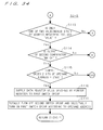
- FIGS. 14 to 19 are flowcharts of control procedures by the buffer controller 26 .
- the buffer controller 26 makes this judgment based on the read/write signal RW.
- a load operation is performed (step S 2 ).
- a store operation is performed (step S 3 ).
- the operand access process completes.
- the load operation S 2 is repeated, the operand address OA is incremented (or decremented) by 1. This accomplishes load operations in one word postincrements (or postdecrements).
- step S 2 The load operation (step S 2 ) is performed in accordance with the flowcharts of FIGS. 15 to 18 , and the store operation (step S 3 ) is performed in accordance with the flowchart of FIG. 19 .
- the buffer controller 26 When the load operation starts, the buffer controller 26 enables the first tri-state buffer 20 and disables the second tri-state buffer 21 (step S 11 ). Then, whether four words specified by the operand address OA are aligned on the word boundary in the data memory 4 is determined according to whether the lower-order two bits U of the operand address OA are 2′b00 (step S 12 ).
- step S 13 When the four words specified by the operand address OA is judged as word-aligned data aligned on the word boundary in the data memory 4 in step S 12 and further the output of the first comparator 261 is a “match” (step S 13 ), the value of the data register 24 is sent to the data bus 62 through the first switch group 23 (step S 14 ).
- the operation of the first and second switches 23 , 22 at this time is shown in FIG. 20, in which only the switches within the ellipse are in the ON position and the others in the OFF position.
- the ellipse means the same in FIGS. 21 to 27 as well.
- step S 13 When the output of the first comparator 261 is a “mismatch” (step S 13 ), the higher-order 28 bits MA 1 of the operand address OA are outputted as the data memory address MA (step S 15 ) and resultant read data is transferred to the data bus 62 through the second switch group 22 (step S 16 ).
- the operation of the first and second switch groups 23 , 22 at this time is shown in FIG. 21 .
- the value of the data register 24 is updated with the read data from the data memory 4 (step S 17 ).
- the aforementioned steps can be performed in a single clock cycle.
- step S 18 , S 20 data held in the data register 24 is outputted through the first switch group 23 and a data memory address MA which addresses data not held in the data register 24 is computed and outputted to the data memory 4 (step S 19 , S 21 ). Resultant read data from the data memory 4 is fed to the second switch group 22 .
- the data memory address MA which addresses data not held in the data register 24 corresponds to: (1) the next higher address following the higher-order 28 bits MA 1 of the operand address OA when the output of the first comparator 261 is a “match”, such an address being obtained by incrementing the higher-order 28 bits MA 1 of the operand address OA by 1 (step S 19 ); and (2) the higher-order 28 bits MA 1 of the operand address OA itself when the output of the second comparator 262 is a “match” (step S 21 ).
- step S 22 the first and second switch groups 23 , 22 are selectively turned on according to the lower-order two bits U of the operand address OA to select four consecutive words of data specified by the operand address OA, then the data is transferred on the data bus 62 to the data path unit 3 .
- the aforementioned steps can be performed in a single clock cycle.
- the operation of the first and second switch groups 23 , 22 in step S 22 depend on the lower-order two bits U of the operand address OA and the outputs of the first and second comparators 261 , 262 as shown in FIGS. 22 to 27 .
- step S 18 When neither the first nor second comparators 261 , 262 indicates a “match” (steps S 18 , S 20 ), data output to the data path unit 3 requires two cycles.
- the higher-order 28 bits MA 1 of the operand address OA are outputted (step S 23 ) and resultant read data is loaded into the data register 24 (step S 25 ).
- step S 24 all the switches in the first and second switch groups 23 , 22 are turned off (step S 24 ), so no data is outputted to the data path unit 3 .
- a wait signal (not shown) for the control unit 1 is generated and one cycle of wait is inserted in the pipeline.
- step S 26 the first comparator 261 always indicates a “match”
- the value obtained by incrementing the higher-order 28 bits MA 1 of the operand address OA is outputted as the data memory address MA (step S 26 ).
- the first switch group 23 selects necessary data from the four words in the data register 24 and the second switch group 22 selects necessary data from the 4-word read data, thereby sending four consecutive words of data specified by the operand address OA to the data path unit 3 (step S 27 ).
- the operation of the first and second switch groups 23 , 22 in step S 27 is shown in FIGS. 22 to 27 .
- step S 3 The buffer controller 26 disables the first tri-state buffer 20 and enables the second tri-state buffer 21 (step S 31 ). Since the data processor of this preferred embodiment does not support data store to operand addresses OA specifying misaligned data in the data memories 4 , 5 , the lower-order two bits U of the operand address OA in a word address format are ignored and the higher-order 28 bits MA 1 are outputted as the data memory address MA to the data memory 4 (step S 32 ). During the store operation (step S 3 ), for the purpose of maintaining coherency between the data memory 4 and the data register 24 , the valid/invalid bit V of the address register 25 is made invalid to disable the value of the data register 24 (step S 33 ).
- the coherency between the data memory 4 and the data register 24 refers to the fact that 4-word data in the data memory 4 corresponding to the data memory address MA held in the address register 25 matches 4-word data held in the data register 24 .
- maintaining the coherency is equivalent to maintaining a set of address and data in the data register 24 and in the address register 25 to always reflect a set of address and data in the data memory 4 .
- step S 3 Since the data register 24 is disabled in the store operation (step S 3 ), even if data in the data memory 4 is rewritten, the values of the address register 25 and the data register 24 will always be updated (step S 17 , S 25 ) at the restart of the load operation (step S 2 ). This prevents the possibility that the value of the data register 24 which does not reflect rewritten data in the data memory 4 is referred to by mistake.
- a load of 4-word data from the data memory 4 to the data path unit 3 can be accomplished in a single cycle irrespective of whether operand data in the load instruction is aligned on the word boundary.
- the load instruction loading misaligned data as operand data can be executed in every one cycle.
- the data processor of the first preferred embodiment can concurrently perform processing such as product-sum operations in the data path unit 3 , updating of the address pointers in the operand-address generation units 8 , 9 , and operand data access to the two data memories 4 , 5 through the alignment buffers 6 , 7 . It also makes it possible to load operand data from the data memories 4 , 5 in a single cycle. Accordingly, product-sum operations can be accomplished with a throughput of a single cycle.
- the data processor of this preferred embodiment achieves FIR processing. It is assumed that the two data memories 4 , 5 store data X and coefficients C, respectively, as shown in FIG. 28 .
- the two data memories 4 , 5 store data X and coefficients C, respectively, as shown in FIG. 28 .
- the increment (or decrement) size of one word allows necessary data to be loaded in a single cycle. This makes it possible to perform product-sum operations with a throughput of a single cycle.
- the data processor of this preferred embodiment can achieve consecutive execution of load instructions holding misaligned data as operand data with a throughput of a single cycle, thereby improving processing speed. Further, there is no need to consider data alignment/misalignment in program development, which improves program development efficiency.
- a data processor of a second preferred embodiment differs from that of the first preferred embodiment in its characteristic that, in the store operation, the value of the data register 24 is updated with write data when the data memory address MA matches the value of the address register 25 . This permits maintenance of coherency without disabling the data register 24 . Therefore, a load of operand data can be accomplished in a single cycle from the beginning of the restart of the load operation.
- FIG. 29 is a flowchart of the procedure of the store operation (step S 3 ) performed by the buffer controller 26 in the data processor of the second preferred embodiment.
- the address held in the address register 25 is compared with the data memory address MA specifying write data (step S 41 ).
- the buffer controller 26 enables not only the first tri-state buffer 20 but also the second tri-state buffer 21 (step S 42 ) and writes data to be written into the data memory 4 , into the data register 24 (step S 43 ).
- step S 44 , 43 When the values mismatch, only writing to the data memory 4 is performed without updating the value of the data register 24 (steps S 44 , 43 ). This store operation can be performed in a single cycle.
- the data register 24 is disabled when consecutive execution of load instructions holding misaligned data as operand data is interrupted to execute the store instruction.
- the first operation requires two cycles.
- the data processor of the second preferred embodiment updates the value of the data register 24 at the same time as data stored in the data memory 4 at the same address as the value of the address register 25 is updated.
- This permits maintenance of coherency between the data memory 4 and the data register 24 without disabling the data register 24 . Since the data register 24 is not disabled, a load of operand data can be accomplished in a single cycle from the beginning of the restart of the load operation. In this fashion, the store operation does not decrease the efficiency of the load operation. Further, the absence of the necessity to disable the data register 24 avoids the necessity for the valid/invalid bit V of the address register 25 ; therefore, the address register can only be 28 bits in length.
- a data processor of a third preferred embodiment comprises alignment buffers, each having two registers to hold data stored at two addresses in the data memory, between the data memory and the data path unit.
- the alignment buffers output word-aligned/misaligned data to the data path unit by selecting operand data from among data held in the two registers, or from among data held in either of the registers and read data from the data memory, or from among read data from the data memory.
- operand addresses width of update
- either of word-aligned or misaligned data can be obtained through a maximum of one access to the data memory.
- consecutive read operations (load operations) handling misaligned data as operand data can be accomplished with a throughput of a single cycle.
- FIG. 30 is a block diagram of a configuration of the alignment buffer 6 according to the third preferred embodiment.
- This alignment buffer 6 differs from that of the first preferred embodiment (FIG. 1) in its characteristic that it further comprises first and second address registers 202 , 203 , first and second data registers 200 , 201 , a selector 205 , a third comparator 265 , a leading pointer register 266 , a first selector 267 , and a second selector 268 .
- the output of the first tri-state buffer 20 is connected in common to the first and second data registers 200 , 201 and the second switch group 22 .
- the outputs of the data registers 200 , 201 are connected to the first switch group 23 through the selector 205 .
- These registers 202 , 203 , 200 , 201 and the selector 205 are also controlled by the buffer controller 26 .
- the buffer controller 26 comprises the first comparator 261 , the second comparator 262 , the third comparator 265 , the incrementer 263 , the leading pointer register 266 , the first selector 267 , and the second selector 268 .
- the value of the leading pointer register 266 indicates which of the two data registers 200 and 201 holds data with the lowest address out of a maximum of eight consecutive words of data.
- the first selector 267 shown in FIG. 31 selects the higher of lower-order 28 bits MA 3 of the first address register 202 and lower-order 28 bits MA 4 of the second address register 203 .
- the second selector 268 selects the lower of the lower-order 28 bits MA 3 of the first address register 202 and the lower-order 28 bits MA 4 of the second address register 203 . Which of the first and second address registers 202 , 203 holds the higher address is determined by the value of the leading pointer register 266 .
- the first comparator 261 makes a comparison between the output of the first selector 267 and the higher-order 28 bits MA 1 of the operand address OA
- the second comparator 262 makes a comparison between the output of the second selector 268 and the higher-order 28 bits MA 1 of the operand address OA by 1.
- the third comparator 265 makes a comparison between the output of the second selector 268 and a value MA 2 obtained by incrementing the higher-order 28 bits MA 1 of the operand address OA by 1.
- the two data registers 200 , 201 are controlled to always hold the values at contiguous data memory addresses. But, this is not the case where either or both of the address registers have the most significant bits or valid/invalid bits V indicating an “invalid”.
- the data register with the highest address out of the consecutive data holds data stored at the head address.
- the value MA 2 obtained by incrementing the higher-order 28 bits MA 1 of the operand address OA by 1 is outputted as the data memory address MA to the data memory 4 , and from among resultant read data and data with the head address held in the register, operand data is selected and outputted to the data path unit 3 .
- the data register with the lowest address holds data stored at the head address. That is, when both of the two data registers 200 , 201 hold valid data, all operand data is held in those registers 200 , 201 . Thus, operand data is selected from among data stored at the head address and data stored at the end address which are held in the two data registers 200 , 201 , and outputted to the data path unit 3 .
- the data register with the lowest address holds data stored at the end address.
- this register holds data stored at the end address plus one and thus operand data is contiguous to the data held in the register. In either case, data stored at the head address is not held in the registers, so the higher-order 28 bits MA 1 of the operand address OA are outputted as the data memory address MA to the data memory 4 .
- operand data is word-aligned data
- resultant read data is sent to the data path unit 3 .
- the operand data is misaligned data, the operand data is selected from among the read data and data stored at the end address which is held in the register, and outputted to the data path unit 3 .
- the higher-order 28 bits MA 1 of the operand address OA are outputted as the data memory address MA to the data memory 4 and resultant read data is stored in one of the data registers.
- the value MA 2 obtained by incrementing the higher-order 28 bits MA 1 of the operand address OA by 1 is outputted to the data memory 4 , and from among resultant read data and data stored at the head address which is held in the register, operand data is selected and outputted to the data path unit 3 .
- FIGS. 32 to 40 show a flow of the load operation (step S 2 ) according to the third preferred embodiment.
- the buffer controller 26 enables the first tri-state buffer 20 and disables the second tri-state buffer 21 (step S 101 ).
- step S 102 it is determined whether both the two valid/invalid bits V of the address registers 202 , 203 indicate an “invalid”.
- a positive judgment result (Yes) in this step indicates that the two data registers 200 , 201 do not hold valid data after initialization of the data processor or after disabled for the execution of the store operation. That is, neither of data stored at the head address and data stored at the end address is held in those registers.
- data stored at the head address is read out (step S 103 ) and the values of the address register specified by the pointer register 266 and the corresponding data register are updated with the read address and the read data (step S 104 ). In this case, this update data will not take effect until the next cycle.
- step S 105 When data to be read is word-aligned data (step S 105 ), the first switch group 23 is turned off and the second switch group 22 is selectively turned on according to the operand address OA, whereby the read data from the data memory 4 is sent to the data path unit 3 (step S 106 ). Then, another data register than that which was updated in step S 104 is disabled (step S 107 ).
- the operation of the second switch group 22 in step S 106 is illustrated in FIG. 41 .
- the processing from steps S 101 to S 107 can be performed in a single cycle.
- step S 105 When data to be read out is misaligned data (step S 105 ), the first and second switch groups are completely turned off (step S 108 ) and a wait signal (not shown) for the control unit 11 is generated to insert one cycle of wait in the pipeline.
- a value obtained by incrementing upper 28 bits of the operand address OA by one is output as a data memory address to read out data stored at the end address from the data memory 4 (step S 109 ).
- step S 110 another address register than that specified by the pointer register 266 , and the corresponding data register are updated with the end address and the read data, respectively.
- step S 112 the value of the data register specified by the pointer register 266 and holding data stored at the head address is supplied to the first switch group 23 (step S 111 ) and the first and second switch groups 23 , 22 are selectively turned on according to the operand address OA and the output of the third comparator 265 to send misaligned data to the data path unit 3 (step S 112 ).
- the processing from steps S 101 to S 112 is performed in two cycles.
- the operation of the first and second switch groups 23 , 22 in step S 112 is illustrated in FIGS. 42 to 44 .
- step S 113 When the judgment result in step S 102 is negative (No), then whether only one of the two valid/invalid bits V of the address registers 202 , 203 indicates a “valid” is determined (step S 113 ). When this judgment result is positive, then whether the value of the address register holding valid data is equal to the head address and whether the same is equal to the end address are determined.
- the second comparator 262 is used for the former judgment (step S 114 ) and the third comparator 265 for the latter (step S 118 ).
- step S 114 When the result in step S 114 is positive, the data register holds data stored at the head address.
- this data register holds all 4-word data specified by the operand address OA since the head address and the end address are equal.
- the value of the data register specified by the leading pointer register 266 is selected and transferred to the first switch group 23 (step S 116 ).
- the second switch group 22 is totally turned off and the first switch group 23 is selectively turned on according to the operand address OA, whereby word-aligned data is sent to the data path unit 3 (step S 117 ).
- the operation of the first switch group 23 in step S 117 is illustrated in FIG. 41 .
- the processing from steps S 101 to S 117 can be performed in a single cycle.
- step S 115 When operand data is misaligned data in step S 115 , the data register holds data stored at the head address, but data stored at the end address is not held. Thus, the steps S 109 to S 112 described before are performed after step S 115 .
- the processing from steps S 101 to S 112 can be performed in a single cycle.
- the operation of the first and second switch groups 23 , 22 in step S 112 is illustrated in FIGS. 42 to 44 .
- step S 114 When the output of the second comparator 262 is a “mismatch” (step S 114 ), then whether the output of the third comparator 265 is a “match” is determined in step S 118 .
- the data register holds data stored at the end address; when the operand address OA specifies word-aligned data, the data register holds data stored at the data memory address obtained by incrementing the end address by 1. In either case, data stored at the head address is not held in the data register.
- upper 28 bits of the operand address OA is output as a data memory address to read out data stored at the head address from the data memory 4 (step S 119 ) and another address register than that specified by the pointer register and the corresponding data register are updated with the head address and the read data, respectively (step S 120 ).
- another data register than that which has held data with the lowest address is updated with data stored at the lower address; therefore, the value of the leading pointer register 266 is updated to indicate another data register than that which had been indicated (step S 121 ).
- step S 122 when the operand address OA specifies word-aligned data (step S 122 ), none of 4-word data specified by the operand address OA is held in the data register since the head address and the end address are equal.
- the first switch group 23 is totally turned off and the second switch group 22 is selectively turned on according to the operand address OA, whereby the data stored at the head address which was read out from the data memory 4 in step S 119 is sent to the data path unit 3 (step S 123 ).
- the operation of the second switch group 22 in step S 123 is illustrated in FIG. 41 .
- the processing from steps S 101 to S 123 can be performed in a single cycle.
- step S 122 When the operand address OA specifies misaligned data in step S 122 , on the other hand, part of 4-word data specified by the operand address OA is not held in the data register. Thus, the value of the data register specified by the pointer register 266 and holding data stored at the end address is sent to the first switch group 23 (step S 124 ) and the data stored at the head address which was read out from the data memory 4 in step S 119 is sent to the second switch group 22 . Then, the first and second switch groups 23 , 22 are selectively turned on according to the operand address OA and the output of the third comparator 265 thereby to send misaligned data to the data path unit 3 (step S 125 ). The processing from steps S 101 to S 125 can be performed in a single cycle. The operation of the first and second switch groups 23 , 22 in step S 125 is illustrated in FIGS. 45 to 47 .
- step S 118 When the output of the third comparator 265 is a “mismatch” in step S 118 , neither of the two data registers 200 , 201 holds data stored at the head address and data stored at the end address. Thus, the processing after step S 103 is performed as in the case where the judgment result in step S 102 is positive.
- step S 113 When the judgment result in step S 113 is negative, both the two data registers 200 , 201 hold valid data and thus which of them holds data stored at the head address is determined in step S 126 .
- the data register with the highest address holds data stored at the head address.
- operand data is word-aligned data (step S 127 )
- this data register holds all 4-word data specified by the operand address OA.
- step S 128 the value of the other data register than that specified by the pointer register 266 , that is, the register holding data stored at the head address is sent to the first switch group 23 (step S 128 ), and the second switch group 22 is turned off and the first switch group 23 is selectively turned on according to the operand address OA, whereby word-aligned data is sent to the data path unit 3 (step S 129 ).
- step S 129 The operation of the first switch group 23 in step S 129 is illustrated in FIG. 41 .
- the processing from steps S 101 to S 129 can be performed in a single cycle.
- step S 127 When operand data is misaligned data according to the judgment result in step S 127 , the two data registers 200 , 201 holds part of data stored at the head address but do not hold data stored at the end address. Thus, data stored at the end address is read out from the data memory 4 (step S 130 ) and the address register specified by the pointer register 266 and the corresponding data register are updated with the end address and the read data, respectively (step S 131 ).
- step S 132 the value of another register specified by the pointer register 266 , that is, the register holding data stored at the head address is supplied to the first switch group 23 (step S 132 ), and the first and second switch groups 23 , 22 are selectively turned on according to the operand address OA and the output of the third comparator 265 (step S 133 ).
- the operation of the first and second switch groups 23 , 22 in step S 133 is illustrated in FIGS. 42 to 44 .
- a register which has held data with the lowest address is updated with data stored at an address which is one address higher than the highest address held in the other register; therefore, the value of the leading pointer register 266 is updated to indicate another register than that which had been indicated (step S 134 ).
- the processing from steps S 101 to S 134 can be performed in a single cycle.
- step S 126 When the output of the first comparator 261 is a “mismatch” in step S 126 , then whether the data register with the lowest address holds data stored at the head address is determined in step S 135 . When the judgment result in step S 135 is positive, the data registers hold both data stored at the head address and data stored at the end address.
- step S 136 when the operand address OA specifies word-aligned data (step S 136 ), the value of the data register specified by the pointer register 266 and holding data stored at the head address is supplied to the first switch group 23 (step S 137 ), and the second switch group 22 is totally turned off and the first switch group 23 is selectively turned on according to the operand address OA, whereby word-aligned data is sent to the data path unit 3 (step S 138 ).
- the operation of the first switch group 23 in step S 138 is illustrated in FIG. 41 .
- the processing from steps S 101 to S 138 can be performed in a single cycle.
- step S 136 When the operand address OA specifies misaligned data (step S 136 ), on the other hand, either of the values of the data register holding data stored the head address and the data register holding data stored at the end address is selected according to the operand address OA as shown in FIG. 48, and transferred to the first switch group 23 (step S 139 ). Then, the second switch group 22 is totally turned off and the first switch group is selectively turned on according to the operand address OA, whereby misaligned data is sent to the data path unit 3 (step S 140 ).
- the operation of the first switch group 23 in step S 140 is illustrated in FIGS. 49 to 51 .
- the processing from steps S 101 to S 140 can be performed in a single cycle.
- the alignment buffer 6 in the data processor of the third preferred embodiment comprises the first and second data registers 200 , 201 to hold data stored at two addresses, wherein 4-word aligned/misaligned data specified by the operand address OA is selected from among a maximum of eight consecutive words of data held in the data registers and 4-word data read from the data memory 4 , and outputted to the data path unit 3 .
- 4-word aligned/misaligned data specified by the operand address OA is selected from among a maximum of eight consecutive words of data held in the data registers and 4-word data read from the data memory 4 , and outputted to the data path unit 3 .
- consecutive execution of load instructions holding misaligned data as operand data can be accomplished not only with a throughput of a single cycle as in the data processor of the first preferred embodiment, but also through a quarter of access times as compared to the data processor of the first preferred embodiment which requires one access to the data memory for every cycle. This saves power consumption in the data memory 4 .
- step S 3 should be performed in the same procedure as that of the first preferred embodiment (FIG. 19) or that of the second preferred embodiment (FIG. 29 ).
- both the first and second data registers 200 , 201 should be disabled by making invalid both the valid/invalid bits V of the first and second address registers 202 , 203 in step S 33 .
- step S 41 it should be judged in step S 41 whether the higher-order 28 bits MA 1 of the operand address OA matches either of the values of the first and second address registers 202 , 203 . Further, in step S 43 , the data to be written into the data memory 4 should also be written into the data register corresponding to the value-matched address register in step S 41 (i.e., either of the first and second data registers 200 , 201 ).
- the present invention can also be applied to those having three data registers by the addition of a comparator.
- the present invention allows any number of data registers in the range of not less than 1.
- judgments are made whether the address registers hold the head address or whether they hold the end address. This makes it possible to perform read operations with a throughput of a single cycle in whichever direction (i.e., plus or minus of the address register value) the operand address OA goes, as long as the increment or decrement size between the operand addresses OA is not more than four words.
- a data processor of a fourth preferred embodiment has two kinds of load instructions: the one which uses the address register 25 and the data register 24 included in the alignment buffer 6 (or 7 ), thereby permitting the reading of consecutive misaligned data with a throughput of a single cycle (the same as the read instruction of the first preferred embodiment); and the one which uses no data register (hereinafter referred to as an “aligned-data read instruction”).
- the aligned-data read instruction is an instruction for loading 4-word data aligned on the word boundary.
- the data processor of the fourth preferred embodiment is identical to that of FIG. 1 , and the alignment buffer 6 is identical to that of FIG. 2 .
- the control unit 1 When operand data access starts, the control unit 1 outputs a control signal indicating the type of instructions to the alignment buffers 6 and 7 , which then operate in accordance with the control signal.
- FIG. 52 is a flowchart of control procedures by the buffer controller 26 according to the fourth preferred embodiment.
- step S 1 When operand data access starts, whether it is a load access or not is determined in step S 1 .
- step S 3 the store operation is performed (step S 3 ).
- the store operation in step S 3 follows the same procedure as in FIG. 19 or 29 .
- step S 80 For load access, whether it is a load using the data register or not is determined (step S 80 ).
- For loads using the data register the same load operation as described in the first preferred embodiment is performed (step S 2 ).
- step S 81 For loads using no data register, an aligned-data load operation is performed at the completion of either operation, the operand access process completes.
- FIG. 53 is a flowchart of the aligned-data load operation (step S 81 ).
- the buffer controller 26 enables the first tri-state buffer 20 and disables the second tri-state buffer 21 (step S 82 ).
- step S 83 the higher-order 28 bits MA 1 of the operand address OA is outputted as the data memory address MA (step S 83 ), and the first switch group 23 is totally turned off and the second switch group 22 is selectively turned on in accordance with the readout of word-aligned data, whereby the read data (word-aligned data) is sent to the data bus 62 through the second switch group 22 (step S 84 ).
- the operation of the first and second switch groups 23 , 22 in step S 84 is identical to that in the case where the lower-order two bits U of the operand address OA are 2′b00 in the load operation (cf. FIGS. 20, 21 ).
- the processing in step S 81 can be performed in a single cycle.
- the values of the data register 24 and the address register 25 are not updated.
- the value of the data register 24 will be updated.
- the first operation immediately after the restart requires two cycles since the value of the data register 24 has been updated with data at another address.
- the data processor of the fourth preferred embodiment can prevent such updating of the data register 24 by executing the aligned-data read instruction using no data register 24 when a load to other memory space is required during execution of the load operation on contiguous operand addresses OA.
- the first operation after the restart of the read instruction can be performed in a single cycle. This improves processing speed.
- a data processor of a fifth preferred embodiment differs from that of the first preferred embodiment in its characteristic that it has a load instruction (hereinafter referred to as a “single-word parallel load instruction”) for loading 1-word data stored in the data memory 4 (or 5 ), which is specified by the operand address OA, in parallel as 4-word data into the data path unit 3 .
- a load instruction hereinafter referred to as a “single-word parallel load instruction” for loading 1-word data stored in the data memory 4 (or 5 ), which is specified by the operand address OA, in parallel as 4-word data into the data path unit 3 .
- the data processor of the fifth preferred embodiment is identical to that in FIG. 1, and the alignment buffer 6 is identical to that in FIG. 2 .
- the control unit 1 When operand data access starts, the control unit 1 outputs a control signal indicating the type of instructions to the alignment buffers 6 and 7 , which then operate in accordance with this control signal.
- FIG. 54 is a flowchart of control procedures by the buffer controller 26 according to the fifth preferred embodiment.
- step S 1 When operand data access starts, whether it is a load access or not is determined in step S 1 .
- the store operation is performed (step S 3 ).
- the store operation in step S 3 follows the same procedure as in FIG. 19 or 29 .
- step S 90 For load access, whether it is an access according to the single-word parallel load instruction or not is determined (step S 90 ).
- the same load instruction as described in the first preferred embodiment is performed (step S 2 ).
- step S 91 For load access according to the single-word parallel load instruction, a single-word parallel load operation is performed at the completion of either operation, the operand access process completes.
- FIG. 55 is a flowchart of the single-word parallel load instruction (step S 91 ).
- the buffer controller 26 enables the first tri-state buffer 20 and disables the second tri-state buffer 21 (step S 92 ).
- the higher-order 28 bits MA 1 of the operand address OA is outputted as the data memory address MA (step S 93 ), and the first switch group 23 is turned off and the second switch group 22 is selectively turned on according to the lower-order two bits U of the operand address OA (step S 94 ). Accordingly, only one word specified by the lower-order two bits U of the operand address OA is selected from the 4-word read data, and the selected one word is sent in parallel as 4-ward data through the second switch group 22 to the data bus 62 .
- step S 94 The operation of the first and second switch groups 23 , 22 in step S 94 is illustrated in FIGS. 56 to 59 .
- FIGS. 56 to 59 only the switches in the ellipse are in the ON position and the others in the OFF position.
- the processing in step S 91 can be performed in a single cycle.
- the data processor of the fifth preferred embodiment When the data processor of the fifth preferred embodiment is used as a FIR filter, the data X and the coefficients C are stored in the space in the data memories 4 , 5 as shown in FIG. 60 .
- each of the coefficients C has to be stored at four locations, unlike the data X, as shown in FIG. 28 .
- the data processor of the fifth preferred embodiment can read out any one word in parallel as 4-word data by using the single-word load instruction, so each of the coefficients C only has to be stored at one location in the data memory 5 as shown in FIG. 60 . That is, the data processor of the fifth preferred embodiment as a FIR filter can reduce the capacity of the data memory 5 to a quarter as compared to that of the first preferred embodiment, thereby saving data memory.
- the buffer controller 26 increments the operand address OA and uses the result for comparison with the address register in the same cycle and generation of the data memory address MA. If the data processor of the first preferred embodiment operates at higher speed, there is a possibility that a series of operations from the output of the operand address OA by the operand-address generation unit 8 , 9 to the reading of data from the data memories 4 , 5 including the generation of the data memory address MA, may not work in a single cycle.
- the alignment buffer 6 comprises a buffer controller 210 having a data memory address register 211 .
- this data memory address register 211 is also updated with the update value of the address register 25 plus one.
- the data memory address register 211 always holds the value held by the address register 25 plus one.
- either of the value of the data memory address register 211 and the lower-order 28 bits MA 1 of the operand address OA is selected and outputted as the data memory address MA. This saves processing time required for the add operation in the first preferred embodiment.
- the update value of the address register 25 minus one is stored in a leading address register 212 in the buffer controller 210 .
- a decrementer 213 is provided for this subtraction.
- the value of the leading address register 212 is fed to one input of the second comparator 262 instead of the lower-order 28 bits MA 3 of the value of the address register 25 used in the first preferred embodiment.
- the other input of the second comparator 262 receives the operand address OA itself instead of the operand address OA plus one used in the first preferred embodiment. With these values, the second comparator 262 can output the same result as in the first preferred embodiment.
- the alignment buffer 6 of the sixth preferred embodiment is identical to that of the first preferred embodiment in FIG. 2 except for the part in FIG. 61 .
- the buffer controller 210 of the sixth preferred embodiment follows the same procedure as the buffer controller 26 of the first preferred embodiment, with the exception that FIGS. 15, 16 , and 18 are replaced with FIGS. 62, 63 , and 64 , respectively
- the procedure of FIG. 62 is identical to that of FIG. 15 except that, in step S 17 , not only the values of the data register 24 and the address register 25 but also the values of the leading address register 212 and the data memory address register 211 are updated (step S 201 ).
- the procedure of FIG. 63 is identical to that of FIG. 16 except that, in step S 19 , the value of the data memory address register 211 is outputted as the data memory address MA (step S 202 ).
- the procedure of FIG. 64 is identical to that of FIG.
- step S 25 not only the values of the data register 24 and the address register 25 but also the values of the leading address register 212 and the data memory address register 211 are updated (step S 203 ) and that, in step S 26 , the value of the data memory address register 211 is outputted as the data memory address MA (step S 204 ).
- the characteristic configuration of the sixth preferred embodiment is also applicable to the data processor of the third preferred embodiment.
- the data memory address register 211 is controlled to have the higher address of the effective data registers 200 , 201 plus one.
- the leading address register 212 is controlled to have the lower address of the effective data registers 200 , 201 minus one. This shortens the time required to read out data from the data memories 4 , 5 as in the first preferred embodiment.
- FIG. 2 of the second preferred embodiment is used as the block diagram of the alignment buffer 6 of the fifth preferred embodiment which performs the single-word parallel load operation
- the configuration of the alignment buffer 6 can be simplified if the load operation in step S 2 is unnecessary in the flowchart of FIG. 54 .
- the first switch group 23 , the data register 24 , and the address register can be deleted from FIG. 2 .
- the first comparator 261 , the second comparator 262 , and the incrementer 263 can be deleted since the buffer controller 26 only needs to output the data memory address MA based on the operand address OA.
Landscapes
- Engineering & Computer Science (AREA)
- Theoretical Computer Science (AREA)
- Software Systems (AREA)
- Physics & Mathematics (AREA)
- General Engineering & Computer Science (AREA)
- General Physics & Mathematics (AREA)
- Advance Control (AREA)
- Executing Machine-Instructions (AREA)
- Memory System (AREA)
Abstract
Description
Claims (11)
Applications Claiming Priority (3)
| Application Number | Priority Date | Filing Date | Title |
|---|---|---|---|
| JP2000040892A JP2001229021A (en) | 2000-02-18 | 2000-02-18 | Data processing device |
| JP2000-040892 | 2000-02-18 | ||
| JPP2000-040892 | 2000-02-18 |
Publications (2)
| Publication Number | Publication Date |
|---|---|
| US20010016898A1 US20010016898A1 (en) | 2001-08-23 |
| US6553474B2 true US6553474B2 (en) | 2003-04-22 |
Family
ID=18564206
Family Applications (1)
| Application Number | Title | Priority Date | Filing Date |
|---|---|---|---|
| US09/767,901 Expired - Fee Related US6553474B2 (en) | 2000-02-18 | 2001-01-24 | Data processor changing an alignment of loaded data |
Country Status (2)
| Country | Link |
|---|---|
| US (1) | US6553474B2 (en) |
| JP (1) | JP2001229021A (en) |
Cited By (8)
| Publication number | Priority date | Publication date | Assignee | Title |
|---|---|---|---|---|
| US20030005255A1 (en) * | 2001-06-29 | 2003-01-02 | Broadcom Corporation | Method and system for fast data access using a memory array |
| US20060085622A1 (en) * | 2004-10-15 | 2006-04-20 | Simone Bartoli | Method and system for managing address bits during buffered program operations in a memory device |
| US20070050592A1 (en) * | 2005-08-31 | 2007-03-01 | Gschwind Michael K | Method and apparatus for accessing misaligned data streams |
| US20080065863A1 (en) * | 2006-09-11 | 2008-03-13 | Eichenberger Alexandre E | Method and apparatus for data stream alignment support |
| US20090037694A1 (en) * | 2007-07-31 | 2009-02-05 | David Arnold Luick | Load Misaligned Vector with Permute and Mask Insert |
| US20120246407A1 (en) * | 2011-03-21 | 2012-09-27 | Hasenplaugh William C | Method and system to improve unaligned cache memory accesses |
| US20130262793A1 (en) * | 2012-03-30 | 2013-10-03 | Intel Corporation | Split-word memory |
| US20190278603A1 (en) * | 2017-03-14 | 2019-09-12 | Samsung Electronics Co., Ltd. | Memory load to load fusing |
Families Citing this family (5)
| Publication number | Priority date | Publication date | Assignee | Title |
|---|---|---|---|---|
| US6912173B2 (en) * | 2001-06-29 | 2005-06-28 | Broadcom Corporation | Method and system for fast memory access |
| US20110087859A1 (en) * | 2002-02-04 | 2011-04-14 | Mimar Tibet | System cycle loading and storing of misaligned vector elements in a simd processor |
| JP3958662B2 (en) * | 2002-09-25 | 2007-08-15 | 松下電器産業株式会社 | Processor |
| US9870318B2 (en) * | 2014-07-23 | 2018-01-16 | Advanced Micro Devices, Inc. | Technique to improve performance of memory copies and stores |
| US20190138308A1 (en) * | 2017-09-15 | 2019-05-09 | MIPS Tech, LLC | Unaligned memory accesses |
Citations (6)
| Publication number | Priority date | Publication date | Assignee | Title |
|---|---|---|---|---|
| JPH0418634A (en) | 1990-05-11 | 1992-01-22 | Mitsubishi Electric Corp | Data processor |
| JPH10161927A (en) | 1996-12-04 | 1998-06-19 | Oki Electric Ind Co Ltd | Load buffer device |
| US5922066A (en) * | 1997-02-24 | 1999-07-13 | Samsung Electronics Co., Ltd. | Multifunction data aligner in wide data width processor |
| US5944775A (en) * | 1994-03-16 | 1999-08-31 | Fujitsu Limited | Sum-of-products arithmetic unit |
| US5961628A (en) * | 1997-01-28 | 1999-10-05 | Samsung Electronics Co., Ltd. | Load and store unit for a vector processor |
| US6266758B1 (en) * | 1997-10-09 | 2001-07-24 | Mips Technologies, Inc. | Alignment and ordering of vector elements for single instruction multiple data processing |
-
2000
- 2000-02-18 JP JP2000040892A patent/JP2001229021A/en active Pending
-
2001
- 2001-01-24 US US09/767,901 patent/US6553474B2/en not_active Expired - Fee Related
Patent Citations (6)
| Publication number | Priority date | Publication date | Assignee | Title |
|---|---|---|---|---|
| JPH0418634A (en) | 1990-05-11 | 1992-01-22 | Mitsubishi Electric Corp | Data processor |
| US5944775A (en) * | 1994-03-16 | 1999-08-31 | Fujitsu Limited | Sum-of-products arithmetic unit |
| JPH10161927A (en) | 1996-12-04 | 1998-06-19 | Oki Electric Ind Co Ltd | Load buffer device |
| US5961628A (en) * | 1997-01-28 | 1999-10-05 | Samsung Electronics Co., Ltd. | Load and store unit for a vector processor |
| US5922066A (en) * | 1997-02-24 | 1999-07-13 | Samsung Electronics Co., Ltd. | Multifunction data aligner in wide data width processor |
| US6266758B1 (en) * | 1997-10-09 | 2001-07-24 | Mips Technologies, Inc. | Alignment and ordering of vector elements for single instruction multiple data processing |
Non-Patent Citations (3)
| Title |
|---|
| DSP56000/DSP560001 Digital Signal Processor User's Manual Motorola, pp. 2-1 to 2-14, "Architectual Overview and Bus Structure". |
| J. Heinrich, MIPS R4000 Microprocessor User's Manual, pp. A102 to A107, "CPU Instruction Set Details," Second Edition. |
| Jim Handy, "The Cache Memory Book," 1998 Academic Press, Second Edition pp. 156-158.* * |
Cited By (20)
| Publication number | Priority date | Publication date | Assignee | Title |
|---|---|---|---|---|
| US6789179B2 (en) * | 2001-06-29 | 2004-09-07 | Broadcom Corporation | Method and system for fast data access using a memory array |
| US20040266027A1 (en) * | 2001-06-29 | 2004-12-30 | Broadcom Corporation | Method and system for fast data access using a memory array |
| US7136985B2 (en) | 2001-06-29 | 2006-11-14 | Broadcom Corporation | Method and system for fast data access using a memory array |
| US20070055832A1 (en) * | 2001-06-29 | 2007-03-08 | Broadom Corporation | Method and system for fast data access using a memory array |
| US7302545B2 (en) | 2001-06-29 | 2007-11-27 | Broadcom Corporation | Method and system for fast data access using a memory array |
| US20030005255A1 (en) * | 2001-06-29 | 2003-01-02 | Broadcom Corporation | Method and system for fast data access using a memory array |
| US20060085622A1 (en) * | 2004-10-15 | 2006-04-20 | Simone Bartoli | Method and system for managing address bits during buffered program operations in a memory device |
| US7404049B2 (en) * | 2004-10-15 | 2008-07-22 | Atmel Corporation | Method and system for managing address bits during buffered program operations in a memory device |
| US20070050592A1 (en) * | 2005-08-31 | 2007-03-01 | Gschwind Michael K | Method and apparatus for accessing misaligned data streams |
| US8156310B2 (en) | 2006-09-11 | 2012-04-10 | International Business Machines Corporation | Method and apparatus for data stream alignment support |
| US20080065863A1 (en) * | 2006-09-11 | 2008-03-13 | Eichenberger Alexandre E | Method and apparatus for data stream alignment support |
| US20090037694A1 (en) * | 2007-07-31 | 2009-02-05 | David Arnold Luick | Load Misaligned Vector with Permute and Mask Insert |
| US7783860B2 (en) * | 2007-07-31 | 2010-08-24 | International Business Machines Corporation | Load misaligned vector with permute and mask insert |
| US20120246407A1 (en) * | 2011-03-21 | 2012-09-27 | Hasenplaugh William C | Method and system to improve unaligned cache memory accesses |
| US20130262793A1 (en) * | 2012-03-30 | 2013-10-03 | Intel Corporation | Split-word memory |
| US8719519B2 (en) * | 2012-03-30 | 2014-05-06 | Intel Corporation | Split-word memory |
| US8924660B2 (en) | 2012-03-30 | 2014-12-30 | Intel Corporation | Split-word memory |
| US9189240B2 (en) | 2012-03-30 | 2015-11-17 | Intel Corporation | Split-word memory |
| US20190278603A1 (en) * | 2017-03-14 | 2019-09-12 | Samsung Electronics Co., Ltd. | Memory load to load fusing |
| US10956155B2 (en) * | 2017-03-14 | 2021-03-23 | Samsung Electronics Co., Ltd. | Memory load to load fusing |
Also Published As
| Publication number | Publication date |
|---|---|
| JP2001229021A (en) | 2001-08-24 |
| US20010016898A1 (en) | 2001-08-23 |
Similar Documents
| Publication | Publication Date | Title |
|---|---|---|
| US5168571A (en) | System for aligning bytes of variable multi-bytes length operand based on alu byte length and a number of unprocessed byte data | |
| KR100267097B1 (en) | Deferred store data read with simple anti-dependency pipeline interlock control in superscalar processor | |
| US7694109B2 (en) | Data processing apparatus of high speed process using memory of low speed and low power consumption | |
| US12455745B2 (en) | Processor subroutine cache | |
| US6553474B2 (en) | Data processor changing an alignment of loaded data | |
| US20250251938A1 (en) | Look-up table write | |
| JPH0477925A (en) | microprocessor | |
| KR102458467B1 (en) | vector creation command | |
| JPH10228376A (en) | Method and program for processing multiple-register instruction | |
| US5335330A (en) | Information processing apparatus with optimization programming | |
| US5710914A (en) | Digital signal processing method and system implementing pipelined read and write operations | |
| US5459847A (en) | Program counter mechanism having selector for selecting up-to-date instruction prefetch address based upon carry signal of adder which adds instruction size and LSB portion of address register | |
| KR100249631B1 (en) | Data processor | |
| JPH07239780A (en) | One-clock variable length instruction execution process type instruction read computer | |
| US4580238A (en) | Arithmetic operating system | |
| US20090037702A1 (en) | Processor and data load method using the same | |
| EP0415351A2 (en) | Data processor for processing instruction after conditional branch instruction at high speed | |
| JP3454393B2 (en) | Data processing device | |
| US5220670A (en) | Microprocessor having ability to carry out logical operation on internal bus | |
| US5649229A (en) | Pipeline data processor with arithmetic/logic unit capable of performing different kinds of calculations in a pipeline stage | |
| JPH0793151A (en) | Instruction supplying device | |
| JPH1173318A (en) | Microprocessor | |
| JP2583614B2 (en) | Vector arithmetic unit | |
| JPS60105050A (en) | Pipeline control system | |
| JPH04130536A (en) | Branching control system |
Legal Events
| Date | Code | Title | Description |
|---|---|---|---|
| AS | Assignment |
Owner name: MITSUBISHI DENKI KABUSHIKI KAISHA, JAPAN Free format text: ASSIGNMENT OF ASSIGNORS INTEREST;ASSIGNORS:ITO, HIRONOBU;SATO, HISAKAZU;REEL/FRAME:011567/0694 Effective date: 20010117 |
|
| FEPP | Fee payment procedure |
Free format text: PAYER NUMBER DE-ASSIGNED (ORIGINAL EVENT CODE: RMPN); ENTITY STATUS OF PATENT OWNER: LARGE ENTITY Free format text: PAYOR NUMBER ASSIGNED (ORIGINAL EVENT CODE: ASPN); ENTITY STATUS OF PATENT OWNER: LARGE ENTITY |
|
| FPAY | Fee payment |
Year of fee payment: 4 |
|
| FPAY | Fee payment |
Year of fee payment: 8 |
|
| AS | Assignment |
Owner name: RENESAS ELECTRONICS CORPORATION, JAPAN Free format text: ASSIGNMENT OF ASSIGNORS INTEREST;ASSIGNOR:MITSUBISHI DENKI KABUSHIKI KAISHA;REEL/FRAME:025980/0219 Effective date: 20110307 |
|
| REMI | Maintenance fee reminder mailed | ||
| LAPS | Lapse for failure to pay maintenance fees | ||
| STCH | Information on status: patent discontinuation |
Free format text: PATENT EXPIRED DUE TO NONPAYMENT OF MAINTENANCE FEES UNDER 37 CFR 1.362 |
|
| STCH | Information on status: patent discontinuation |
Free format text: PATENT EXPIRED DUE TO NONPAYMENT OF MAINTENANCE FEES UNDER 37 CFR 1.362 |
|
| FP | Lapsed due to failure to pay maintenance fee |
Effective date: 20150422 |