US6515642B1 - Driving circuit for a liquid crystal display - Google Patents

Driving circuit for a liquid crystal display Download PDF

Info

Publication number
US6515642B1
US6515642B1 US09/417,683 US41768399A US6515642B1 US 6515642 B1 US6515642 B1 US 6515642B1 US 41768399 A US41768399 A US 41768399A US 6515642 B1 US6515642 B1 US 6515642B1
Authority
US
United States
Prior art keywords
terminal
liquid crystal
crystal display
dynamic controller
dynamic
Prior art date
Legal status (The legal status is an assumption and is not a legal conclusion. Google has not performed a legal analysis and makes no representation as to the accuracy of the status listed.)
Expired - Lifetime
Application number
US09/417,683
Inventor
Vincent Lin
Current Assignee (The listed assignees may be inaccurate. Google has not performed a legal analysis and makes no representation or warranty as to the accuracy of the list.)
138 East LCD Advancements Ltd
Original Assignee
Seiko Epson Corp
Priority date (The priority date is an assumption and is not a legal conclusion. Google has not performed a legal analysis and makes no representation as to the accuracy of the date listed.)
Filing date
Publication date
Application filed by Seiko Epson Corp filed Critical Seiko Epson Corp
Priority to US09/417,683 priority Critical patent/US6515642B1/en
Assigned to SEIKO EPSON CORPORATION reassignment SEIKO EPSON CORPORATION ASSIGNMENT OF ASSIGNORS INTEREST (SEE DOCUMENT FOR DETAILS). Assignors: LIN, VINCENT
Priority to TW089121487A priority patent/TW558706B/en
Priority to JP2000315828A priority patent/JP2001159885A/en
Application granted granted Critical
Publication of US6515642B1 publication Critical patent/US6515642B1/en
Assigned to 138 EAST LCD ADVANCEMENTS LIMITED reassignment 138 EAST LCD ADVANCEMENTS LIMITED ASSIGNMENT OF ASSIGNORS INTEREST (SEE DOCUMENT FOR DETAILS). Assignors: SEIKO EPSON CORPORATION
Anticipated expiration legal-status Critical
Expired - Lifetime legal-status Critical Current

Links

Images

Classifications

    • GPHYSICS
    • G09EDUCATION; CRYPTOGRAPHY; DISPLAY; ADVERTISING; SEALS
    • G09GARRANGEMENTS OR CIRCUITS FOR CONTROL OF INDICATING DEVICES USING STATIC MEANS TO PRESENT VARIABLE INFORMATION
    • G09G3/00Control arrangements or circuits, of interest only in connection with visual indicators other than cathode-ray tubes
    • G09G3/20Control arrangements or circuits, of interest only in connection with visual indicators other than cathode-ray tubes for presentation of an assembly of a number of characters, e.g. a page, by composing the assembly by combination of individual elements arranged in a matrix no fixed position being assigned to or needed to be assigned to the individual characters or partial characters
    • G09G3/34Control arrangements or circuits, of interest only in connection with visual indicators other than cathode-ray tubes for presentation of an assembly of a number of characters, e.g. a page, by composing the assembly by combination of individual elements arranged in a matrix no fixed position being assigned to or needed to be assigned to the individual characters or partial characters by control of light from an independent source
    • G09G3/36Control arrangements or circuits, of interest only in connection with visual indicators other than cathode-ray tubes for presentation of an assembly of a number of characters, e.g. a page, by composing the assembly by combination of individual elements arranged in a matrix no fixed position being assigned to or needed to be assigned to the individual characters or partial characters by control of light from an independent source using liquid crystals
    • G09G3/3611Control of matrices with row and column drivers
    • G09G3/3696Generation of voltages supplied to electrode drivers
    • GPHYSICS
    • G09EDUCATION; CRYPTOGRAPHY; DISPLAY; ADVERTISING; SEALS
    • G09GARRANGEMENTS OR CIRCUITS FOR CONTROL OF INDICATING DEVICES USING STATIC MEANS TO PRESENT VARIABLE INFORMATION
    • G09G3/00Control arrangements or circuits, of interest only in connection with visual indicators other than cathode-ray tubes
    • G09G3/20Control arrangements or circuits, of interest only in connection with visual indicators other than cathode-ray tubes for presentation of an assembly of a number of characters, e.g. a page, by composing the assembly by combination of individual elements arranged in a matrix no fixed position being assigned to or needed to be assigned to the individual characters or partial characters
    • G09G3/34Control arrangements or circuits, of interest only in connection with visual indicators other than cathode-ray tubes for presentation of an assembly of a number of characters, e.g. a page, by composing the assembly by combination of individual elements arranged in a matrix no fixed position being assigned to or needed to be assigned to the individual characters or partial characters by control of light from an independent source
    • G09G3/36Control arrangements or circuits, of interest only in connection with visual indicators other than cathode-ray tubes for presentation of an assembly of a number of characters, e.g. a page, by composing the assembly by combination of individual elements arranged in a matrix no fixed position being assigned to or needed to be assigned to the individual characters or partial characters by control of light from an independent source using liquid crystals
    • G09G3/3611Control of matrices with row and column drivers
    • G09G3/3622Control of matrices with row and column drivers using a passive matrix

Definitions

  • This invention relates for a driving circuit for a liquid crystal display, and more particularly, to a dynamic controller located in a driving circuit for a liquid crystal display to stabilize the supply voltage.
  • a plurality of common signals in the horizontal axis are inter-connected with a plurality of segment signals in the vertical axis.
  • the voltage levels of the common signals and the segment signals are each divided into several predetermined voltage levels, such as Vdd, VL 1 , VL 2 and VL 3 , as shown in FIG. 1 .
  • Vdd is a voltage pair of VL 2 .
  • VL 1 is a voltage pair of VL 3 .
  • corresponding liquid crystal cells of the liquid crystal display will be respectively polarized or not polarized by changing the parasitic capacitors in the liquid crystal display.
  • the upper input voltage level of the parasitic capacitor is controller by the common signals via the analog switches
  • the input voltage of the parasitic capacitor is controller by the segment signals via the analog switches.
  • a frame frequency, shown in FIG. 2 is constructed by a negative cycle where the valid input voltage levels of the segment signals are all negative and by a positive cycle where the valid input voltage levels of the segment signals are all positive.
  • the common signals can be regarded as being scanned in a manner as follows.
  • the common signals are switched between Vdd and VL 2
  • the common signals are switched between VL 1 and VL 3 .
  • the common signal with the voltage level Vdd means that the common signal is being scanned.
  • the common signal with the voltage level VL 3 means that the common signal is being scanned.
  • the voltage difference between the common signal and the segment signal at the moment will determine the voltage difference of the liquid crystal cell.
  • Another conventional solution for the varied voltage level is to construct a divided circuit by setting a plurality of resistors. As shown in FIG. 4, a plurality of resistors are biased between the drain supply voltage, Vdd, and the source supply voltage. Each interconnection point between two conjunct resistors derives an individual voltage level.
  • the driving voltage level of the liquid crystal display is combined by these derived voltage levels and the drain supply voltage level.
  • This conventional driving circuit has the drawback of consuming a large current, and of the area driven by the driving circuit being limited, for example, 10 ⁇ A to drive the area of 5 cm ⁇ 2 cm of the liquid crystal display.
  • the object according to this invention is to overcome the drawbacks of the two conventional driving circuits for the liquid crystal display by constructing a plurality of dynamic controllers in a driving circuit for a liquid crystal display.
  • the dynamic controller according to this invention is able to eliminate the necessity of the installation of the external capacitors for the conventional driving circuit and significantly reducing the driving current for the driving circuit. Also, the dynamic controller can drive a much larger area for a liquid crystal panel.
  • the power saving function according to this invention is achieved by timely emitting the power-on signal once at the moment before and after each of the common signals is to be scanned so as to properly enable the Schmitt comparator.
  • Each dynamic controller of the driving circuit for the liquid crystal display in this invention is to keep the input voltage level steady in such a manner that when the output voltage of the dynamic controller is too large, the sink current in the dynamic controller will lower the output voltage level, and when the output voltage of the dynamic controller is too small, the Schmitt comparator in the dynamic controller will raise the output voltage level.
  • FIG. 1 shows a conventional configuration of the common signals, segment signals, divided voltage levels and liquid crystal cells
  • FIG. 2 is a timing diagram for the common signals and the segment signals of the prior art
  • FIG. 3 shows a configuration of installing capacitors for the conventional driving circuit for the liquid crystal display
  • FIG. 4 shows a conventional divided circuit with a plurality of resistors for the driving circuit for the liquid crystal display
  • FIG. 5 shows a dynamic controller connected in the divided circuit with a plurality of resistor for the driving circuit for the liquid crystal display according to this invention
  • FIG. 6 is a circuit diagram of the dynamic controller of the driving circuit for the liquid crystal display according to this invention.
  • FIG. 7 shows a timing diagrams of the power-on signal and the common signal for the Schmitt comparator of the dynamic controller of the driving circuit for the liquid crystal display according to this invention.
  • FIG. 5 The arrangement of dynamic controllers according to this invention is shown in FIG. 5 .
  • the input side of the dynamic controller is connected to the interconnection between two conjunct resistors of the conventional divided circuit with a plurality of resistors as shown in FIG. 4 .
  • each operating amplifier will consume 1.5 ⁇ A, and there is two operating amplifiers for consuming 3 ⁇ A.
  • Each Schmitt comparator consumes 1 ⁇ A.
  • the consuming current that is 4 ⁇ A, can drive an area of 5 cm ⁇ 5 cm of a liquid crystal display.
  • the driving current in this invention is only 40% of the conventional driving current, and the driven area according to this invention is about two and a half times of the conventional driven area as shown in FIG.
  • the goal of driving a larger area of the liquid crystal display with a smaller current is achieved.
  • the object of further saving the power is achieved by timely emitting the power-on signal for enabling the dynamic controller such that the drawbacks of the conventional capacitor type and resistor type of the driving circuits can be solved.
  • the driving circuit for the liquid crystal display is to connect each input terminal of a plurality of dynamic controllers between the conjunct resistors of a resister type divided voltage circuit having a plurality of resistors, wherein the positive and negative terminals of the divided voltage circuit are respectively connected to the drain supply terminal and the source supply terminal of the driving circuit.
  • the detailed circuit diagram of the dynamic controller according to the embodiment according to this invention is shown in FIG. 6 .
  • the dynamic controller according to this invention mainly comprises an operating amplifier, a Schmitt comparator and a plurality of NMOS transistors used as switches.
  • the dynamic controller is driven by a small current to keep the output voltage level equal to the input voltage level.
  • the reference numeral 1 indicates a CMOS differential amplifier.
  • the input voltage level (Vi) and the output voltage level (Vo) of the amplifier 1 are the voltage levels that this invention intends to keep them equal with each other.
  • a first PMOS transistor 5 is connected to the output voltage terminal.
  • the load of the CMOS differential amplifier 1 is a second PMOS transistor.
  • the gate terminal of the first PMOS transistor 5 is connected to the gate terminal of the second PMOS transistor, both being supplied with a constant source voltage.
  • the positive voltage shown in FIG. 5 could be in +3 volts.
  • the reference numeral 2 in FIG. 6 is a Schmitt comparator.
  • the two input terminals of the comparator 2 are respectively connected with the input voltage terminal and output voltage terminal of the dynamic controller.
  • Two strobe terminals of the comparator 2 are respectively connected to the drain supply terminal and to the drain terminal of a second NMOS transistor 4 for acting as a switch.
  • the source terminal and gate terminal of the second NMOS transistor 4 are respectively connected to the output terminal of the dynamic controller and to a power-on signal of the dynamic controller.
  • the output terminal of the comparator 2 is connected to a gate terminal of a third PMOS transistor, also called MP 1 .
  • the source terminal of the transistor MP 1 is connected to the output voltage (Vo) terminal of the dynamic controller via a current control transistor.
  • the reference numeral 3 in FIG. 6 indicates a first NMOS transistor.
  • the drain terminal, source terminal, and gate terminal of the first NMOS transistor 3 are, respectively, connected to the output terminal of the dynamic controller, the source supply terminal of the dynamic controller, and the source terminal of the PMOS transistor of the CMOS differential amplifier 1 , in which the gate terminal of the PMOS transistor is connected to the input terminal of the dynamic controller.
  • the CMOS differential amplifier 1 including the second PMOS transistor acting as a load
  • the first PMOS transistor 5 and the first NMOS transistor 3 are integrally called an operating amplifier (OP AMP) according to this invention.
  • the CMOS transistor of the CMOS differential amplifier 1 of the operating amplifier has the characteristic feature that the current is only consumed at the moment of switching the input voltage level. Furthermore, the CMOS differential amplifier 1 is capable of transmitting the same input voltage level as the level at the output voltage terminal. Therefore, the CMOS differential amplifier 1 is able to keep the desired voltage in the output voltage terminal in a manner of consuming a rather small current by using the characteristic feature of the sink current and the Schmitt comparator when the input voltage level is varied. In other words, the output voltage level and the input voltage level can be kept equal with each other by a rather small driving current.
  • the dynamic controller when the input voltage level is varied by the change of the common signal or the segment signal, the principle of keeping the output voltage level the same as the input voltge level is as follows.
  • the output voltage level (Vo) When the output voltage level (Vo) is higher than the desired voltage level, since the first NMOS transistor 3 is activated by the high output voltage level, the sink current in the first NMOS transistor 3 will immediately lower the output voltage level to the desired voltage level.
  • the Schmitt comparator when the output voltage level is lower than the input voltage level, since the Schmitt comparator will compare the value of the output voltage level with that of the input voltage level and at this moment will decide that the output voltage level of the Schmitt comparator should be in the output voltage level so as to enable the third PMOS transistor MP 1 , therefore, the output voltage level is raised to the proper higher voltage level.
  • the power-on signal of the dynamic controller according to this invention can be activated once at the period before and after while each common signal of the liquid crystal display is to be activated.
  • the reason for only emitting the power-on signal once in the period of changing the level of the common signal is that the output voltage level of the dynamic controller varies once when each of the common signals is changed, as shown in FIG. 7 .

Landscapes

  • Engineering & Computer Science (AREA)
  • Chemical & Material Sciences (AREA)
  • Crystallography & Structural Chemistry (AREA)
  • Physics & Mathematics (AREA)
  • Computer Hardware Design (AREA)
  • General Physics & Mathematics (AREA)
  • Theoretical Computer Science (AREA)
  • Liquid Crystal Display Device Control (AREA)
  • Control Of Indicators Other Than Cathode Ray Tubes (AREA)
  • Liquid Crystal (AREA)

Abstract

This invention relates to a driving circuit for a liquid crystal display, comprising a plurality of dynamic controllers, each dynamic controller including the integration of an operating amplifier, a Schmitt comparator and a plurality of transistors acting as switches.

Description

BACKGROUND OF THE INVENTION
1. Field of the Invention
This invention relates for a driving circuit for a liquid crystal display, and more particularly, to a dynamic controller located in a driving circuit for a liquid crystal display to stabilize the supply voltage.
2. Description of Prior Art
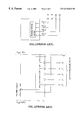
For a small-scale liquid crystal display of a liquid crystal device such as a watch, a timer and a meter, a plurality of common signals in the horizontal axis are inter-connected with a plurality of segment signals in the vertical axis. The voltage levels of the common signals and the segment signals are each divided into several predetermined voltage levels, such as Vdd, VL1, VL2 and VL3, as shown in FIG. 1. Taking the example of the voltage levels of Vdd, VL1, VL2 and VL3, Vdd is a voltage pair of VL2. Likewise, VL1 is a voltage pair of VL3. By the operation of opening or closing several analog switches in FIG. 1, corresponding liquid crystal cells of the liquid crystal display will be respectively polarized or not polarized by changing the parasitic capacitors in the liquid crystal display. In the upper portion of FIG. 1, the upper input voltage level of the parasitic capacitor is controller by the common signals via the analog switches, and, in the lower portion of FIG. 1, the input voltage of the parasitic capacitor is controller by the segment signals via the analog switches. A frame frequency, shown in FIG. 2, is constructed by a negative cycle where the valid input voltage levels of the segment signals are all negative and by a positive cycle where the valid input voltage levels of the segment signals are all positive. The common signals can be regarded as being scanned in a manner as follows. In the negative cycle of the frame frequency, the common signals are switched between Vdd and VL2, and in the positive cycle of the frame frequency, the common signals are switched between VL1 and VL3. In the negative cycle, the common signal with the voltage level Vdd means that the common signal is being scanned. In the positive cycle, the common signal with the voltage level VL3 means that the common signal is being scanned. The voltage difference between the common signal and the segment signal at the moment will determine the voltage difference of the liquid crystal cell. As shown in FIG. 2, there are four common signals, and hence each portion of the negative and positive cycle of the frame frequency is divided into four pieces. In each divided cycle of the negative cycle, if the segment signal of the scanned common signal is VL3, since the voltage difference between the common signal and the segment signal is large, the liquid crystal cell will be turned on. In the same manner, in each divided cycle of the positive cycle, if the segment signal of the scanned common signal is Vdd, since the voltage difference between the common signal and the segment signal is large, the liquid crystal cell will be turned on. Otherwise, the liquid crystal cell will be turned off By multiplexing the liquid crystal cell to different voltage levels, the varied levels will cause the problem of floating the input voltage of the liquid crystal cell. The conventional solution for solving this problem is to provide a capacitor connected between the corresponding input level and the ground, as shown in FIG. 3, for achieving the goal of raising the voltage level and further stabilizing the voltage level. However, the installation of the capacitors will result in the problems of having too many pins for the integrated circuit, the area need for the integral layout being too large, and causing the trouble for preparing the capacitors. Another conventional solution for the varied voltage level is to construct a divided circuit by setting a plurality of resistors. As shown in FIG. 4, a plurality of resistors are biased between the drain supply voltage, Vdd, and the source supply voltage. Each interconnection point between two conjunct resistors derives an individual voltage level. The driving voltage level of the liquid crystal display is combined by these derived voltage levels and the drain supply voltage level. This conventional driving circuit has the drawback of consuming a large current, and of the area driven by the driving circuit being limited, for example, 10 μA to drive the area of 5 cm×2 cm of the liquid crystal display.
SUMMARY OF THE INVENTION
The object according to this invention is to overcome the drawbacks of the two conventional driving circuits for the liquid crystal display by constructing a plurality of dynamic controllers in a driving circuit for a liquid crystal display. The dynamic controller according to this invention is able to eliminate the necessity of the installation of the external capacitors for the conventional driving circuit and significantly reducing the driving current for the driving circuit. Also, the dynamic controller can drive a much larger area for a liquid crystal panel. The power saving function according to this invention is achieved by timely emitting the power-on signal once at the moment before and after each of the common signals is to be scanned so as to properly enable the Schmitt comparator.
Each dynamic controller of the driving circuit for the liquid crystal display in this invention is to keep the input voltage level steady in such a manner that when the output voltage of the dynamic controller is too large, the sink current in the dynamic controller will lower the output voltage level, and when the output voltage of the dynamic controller is too small, the Schmitt comparator in the dynamic controller will raise the output voltage level.
BRIEF DESCRIPTION OF THE DRAWINGS
FIG. 1 shows a conventional configuration of the common signals, segment signals, divided voltage levels and liquid crystal cells;
FIG. 2 is a timing diagram for the common signals and the segment signals of the prior art;
FIG. 3 shows a configuration of installing capacitors for the conventional driving circuit for the liquid crystal display;
FIG. 4 shows a conventional divided circuit with a plurality of resistors for the driving circuit for the liquid crystal display;
FIG. 5 shows a dynamic controller connected in the divided circuit with a plurality of resistor for the driving circuit for the liquid crystal display according to this invention;
FIG. 6 is a circuit diagram of the dynamic controller of the driving circuit for the liquid crystal display according to this invention; and
FIG. 7 shows a timing diagrams of the power-on signal and the common signal for the Schmitt comparator of the dynamic controller of the driving circuit for the liquid crystal display according to this invention.
DETAILED DESCRIPTION OF THE PREFERRED EMBODIMENT
By referring to the drawings, a preferred embodiment according to this invention will be described as follows.
The arrangement of dynamic controllers according to this invention is shown in FIG. 5. The input side of the dynamic controller is connected to the interconnection between two conjunct resistors of the conventional divided circuit with a plurality of resistors as shown in FIG. 4. In view of the current consumed in the dynamic controller according to this invention, each operating amplifier will consume 1.5 μA, and there is two operating amplifiers for consuming 3 μA. Each Schmitt comparator consumes 1 μA. Totally, the consuming current, that is 4 μA, can drive an area of 5 cm×5 cm of a liquid crystal display. It is clear that the driving current in this invention is only 40% of the conventional driving current, and the driven area according to this invention is about two and a half times of the conventional driven area as shown in FIG. 3. Thus, the goal of driving a larger area of the liquid crystal display with a smaller current is achieved. The object of further saving the power is achieved by timely emitting the power-on signal for enabling the dynamic controller such that the drawbacks of the conventional capacitor type and resistor type of the driving circuits can be solved.
Referring to FIG. 5, the driving circuit for the liquid crystal display according to this invention is to connect each input terminal of a plurality of dynamic controllers between the conjunct resistors of a resister type divided voltage circuit having a plurality of resistors, wherein the positive and negative terminals of the divided voltage circuit are respectively connected to the drain supply terminal and the source supply terminal of the driving circuit.
The detailed circuit diagram of the dynamic controller according to the embodiment according to this invention is shown in FIG. 6. The dynamic controller according to this invention mainly comprises an operating amplifier, a Schmitt comparator and a plurality of NMOS transistors used as switches. The dynamic controller is driven by a small current to keep the output voltage level equal to the input voltage level.
Referring to FIG. 6, the reference numeral 1 indicates a CMOS differential amplifier. The input voltage level (Vi) and the output voltage level (Vo) of the amplifier 1 are the voltage levels that this invention intends to keep them equal with each other. A first PMOS transistor 5 is connected to the output voltage terminal. The load of the CMOS differential amplifier 1 is a second PMOS transistor. The gate terminal of the first PMOS transistor 5 is connected to the gate terminal of the second PMOS transistor, both being supplied with a constant source voltage. The positive voltage shown in FIG. 5 could be in +3 volts. The reference numeral 2 in FIG. 6 is a Schmitt comparator. The two input terminals of the comparator 2 are respectively connected with the input voltage terminal and output voltage terminal of the dynamic controller. Two strobe terminals of the comparator 2 are respectively connected to the drain supply terminal and to the drain terminal of a second NMOS transistor 4 for acting as a switch. The source terminal and gate terminal of the second NMOS transistor 4 are respectively connected to the output terminal of the dynamic controller and to a power-on signal of the dynamic controller. The output terminal of the comparator 2 is connected to a gate terminal of a third PMOS transistor, also called MP1. The source terminal of the transistor MP1 is connected to the output voltage (Vo) terminal of the dynamic controller via a current control transistor. The reference numeral 3 in FIG. 6 indicates a first NMOS transistor. The drain terminal, source terminal, and gate terminal of the first NMOS transistor 3 are, respectively, connected to the output terminal of the dynamic controller, the source supply terminal of the dynamic controller, and the source terminal of the PMOS transistor of the CMOS differential amplifier 1, in which the gate terminal of the PMOS transistor is connected to the input terminal of the dynamic controller. In FIG. 6, the CMOS differential amplifier 1 (including the second PMOS transistor acting as a load), the first PMOS transistor 5, and the first NMOS transistor 3 are integrally called an operating amplifier (OP AMP) according to this invention.
The operation principle of the dynamic controller in the driving circuit for the liquid crystal display is as follows:
According to the dynamic controller in the preferred embodiment according to this invention, the CMOS transistor of the CMOS differential amplifier 1 of the operating amplifier has the characteristic feature that the current is only consumed at the moment of switching the input voltage level. Furthermore, the CMOS differential amplifier 1 is capable of transmitting the same input voltage level as the level at the output voltage terminal. Therefore, the CMOS differential amplifier 1 is able to keep the desired voltage in the output voltage terminal in a manner of consuming a rather small current by using the characteristic feature of the sink current and the Schmitt comparator when the input voltage level is varied. In other words, the output voltage level and the input voltage level can be kept equal with each other by a rather small driving current.
According to the dynamic controller in the preferred embodiment of the invention, when the input voltage level is varied by the change of the common signal or the segment signal, the principle of keeping the output voltage level the same as the input voltge level is as follows.
When the output voltage level (Vo) is higher than the desired voltage level, since the first NMOS transistor 3 is activated by the high output voltage level, the sink current in the first NMOS transistor 3 will immediately lower the output voltage level to the desired voltage level. On the other hand, when the output voltage level is lower than the input voltage level, since the Schmitt comparator will compare the value of the output voltage level with that of the input voltage level and at this moment will decide that the output voltage level of the Schmitt comparator should be in the output voltage level so as to enable the third PMOS transistor MP1, therefore, the output voltage level is raised to the proper higher voltage level.
Furthermore, in the preferred embodiment according to this invention, in order to further save the power, the power-on signal of the dynamic controller according to this invention can be activated once at the period before and after while each common signal of the liquid crystal display is to be activated. The reason for only emitting the power-on signal once in the period of changing the level of the common signal is that the output voltage level of the dynamic controller varies once when each of the common signals is changed, as shown in FIG. 7.
Although the present invention and its advantages have been described in detail, it should be understood that various changes, substitutions and alterations, such as changing the N-type substrate according to this invention to the P-type substrate, can be made without departing from the spirit and scope of the invention as defined by the appended claims.

Claims (5)

What is claimed is:
1. A driving circuit for a liquid crystal display, comprising a plurality of dynamic controllers, each dynamic controller comprising:
an operating amplifier including a CMOS differential amplifier, a first PMOS transistor (5) and a first NMOS transistor (3), wherein a load of the CMOS differential amplifier is a second PMOS transistor, a gate terminal of the second PMOS transistor and a gate terminal of the first PMOS transistor are connected with each other with the supply of a constant source voltage thereto, drain terminals of the first and second PMOS transistors are both connected to a drain supply voltage terminal of the dynamic controller, a source terminal of the first PMOS transistor and a drain terminal of the first NMOS transistor are both connected to an output voltage (Vo) terminal of the dynamic controller, and source terminals of the first NMOS transistor and the CMOS differential amplifier are both connected to a source power voltage terminal of the dynamic controller; and
a Schmitt comparator of which a positive comparing terminal and a negative comparing terminal are connected to the output voltage (Vo) terminal and an input voltage (Vi) terminal of the dynamic controller, respectively, an output voltage terminal of the comparator is connected to a gate terminal of a third PMOS transistor (MP1) acting as a switch, the gate terminal of the third PMOS transistor is connected to the drain supply voltage terminal of the dynamic controller, a source terminal of the third PMOS transistor is connected to the output voltage (Vo) terminal via a current control resistor, two strobe terminals of the Schmitt comparator are connected to the drain supply voltage terminal of the dynamic controller and a drain terminal of a second NMOS transistor, respectively, and a gate terminal and a source terminal of the second NMOS transistor are connected to a power-on signal terminal and the output voltage (Vo) terminal of the dynamic controller, respectively.
2. A driving circuit for a liquid crystal display claimed in claim 1, wherein a power-on signal of the dynamic controller is activated at the period before and after while each common signal of the liquid crystal display is to be activated.
3. A driving circuit for a liquid crystal display claimed in claim 1, wherein a power-on signal of the dynamic controllers is activated at the period before and after while each common signal of the liquid crystal display is to be activated, and a drain terminal, a gate terminal and a source terminal of a N-MOS transistor is connected with the output voltage terminal of the circuit, a source terminal of input-side P-MOS transistor of an operating amplifier, and a source power voltage terminal.
4. A driving circuit for a liquid crystal display, comprising a plurality of dynamic controllers, each dynamic controller including an operating amplifier, a Schmitt comparator and a plurality of transistors acting as switches for keeping an output voltage level of the dynamic controller equal to an input voltage level of the dynamic controller, wherein a power-on signal of the dynamic controllers is activated at the period before and after while each common signal of the liquid crystal display is to be activated.
5. A driving circuit for a liquid crystal display, comprising a plurality of dynamic controllers, each dynamic controller including an operating amplifier, a Schmitt comparator and a plurality of transistors acting as switches for keeping an output voltage level of the dynamic controller equal to an input voltage level of the dynamic controller, wherein a power-on signal of the dynamic controllers is activated at the period before and after while each common signal of the liquid crystal display is to be activated, and a drain terminal, a gate terminal and a source terminal of a N-MOS transistor is connected with the output voltage terminal of the circuit, a source terminal of input-side P-MOS transistor of an operating amplifier, and a source power voltage terminal.
US09/417,683 1999-10-14 1999-10-14 Driving circuit for a liquid crystal display Expired - Lifetime US6515642B1 (en)

Priority Applications (3)

Application Number Priority Date Filing Date Title
US09/417,683 US6515642B1 (en) 1999-10-14 1999-10-14 Driving circuit for a liquid crystal display
TW089121487A TW558706B (en) 1999-10-14 2000-10-13 Driving circuit for a liquid crystal display
JP2000315828A JP2001159885A (en) 1999-10-14 2000-10-16 Drive circuit for liquid crystal display

Applications Claiming Priority (1)

Application Number Priority Date Filing Date Title
US09/417,683 US6515642B1 (en) 1999-10-14 1999-10-14 Driving circuit for a liquid crystal display

Publications (1)

Publication Number Publication Date
US6515642B1 true US6515642B1 (en) 2003-02-04

Family

ID=23654984

Family Applications (1)

Application Number Title Priority Date Filing Date
US09/417,683 Expired - Lifetime US6515642B1 (en) 1999-10-14 1999-10-14 Driving circuit for a liquid crystal display

Country Status (3)

Country Link
US (1) US6515642B1 (en)
JP (1) JP2001159885A (en)
TW (1) TW558706B (en)

Cited By (2)

* Cited by examiner, † Cited by third party
Publication number Priority date Publication date Assignee Title
US20080094007A1 (en) * 2006-10-19 2008-04-24 Richtek Technology Corporation Backlight control circuit
US20130050083A1 (en) * 2011-08-24 2013-02-28 Pixart Imaging Inc. Human interface device

Citations (6)

* Cited by examiner, † Cited by third party
Publication number Priority date Publication date Assignee Title
US5869999A (en) * 1996-04-17 1999-02-09 Mitutoyo Corporation Open loop pre-amplifier for an electronic measuring system
US6008669A (en) * 1996-06-19 1999-12-28 Stmicroelectronics Gmbh Monolithic integrated multiple mode circuit
US6057819A (en) * 1996-08-28 2000-05-02 Alps Electric Co., Ltd. Liquid crystal display apparatus and drive circuitry used in the same apparatus
US6118415A (en) * 1998-04-10 2000-09-12 Eldec Corporation Resonant square wave fluorescent tube driver
US6124843A (en) * 1995-01-30 2000-09-26 Olympus Optical Co., Ltd. Head mounting type image display system
US6201517B1 (en) * 1997-02-27 2001-03-13 Minolta Co., Ltd. Stereoscopic image display apparatus

Patent Citations (6)

* Cited by examiner, † Cited by third party
Publication number Priority date Publication date Assignee Title
US6124843A (en) * 1995-01-30 2000-09-26 Olympus Optical Co., Ltd. Head mounting type image display system
US5869999A (en) * 1996-04-17 1999-02-09 Mitutoyo Corporation Open loop pre-amplifier for an electronic measuring system
US6008669A (en) * 1996-06-19 1999-12-28 Stmicroelectronics Gmbh Monolithic integrated multiple mode circuit
US6057819A (en) * 1996-08-28 2000-05-02 Alps Electric Co., Ltd. Liquid crystal display apparatus and drive circuitry used in the same apparatus
US6201517B1 (en) * 1997-02-27 2001-03-13 Minolta Co., Ltd. Stereoscopic image display apparatus
US6118415A (en) * 1998-04-10 2000-09-12 Eldec Corporation Resonant square wave fluorescent tube driver

Cited By (4)

* Cited by examiner, † Cited by third party
Publication number Priority date Publication date Assignee Title
US20080094007A1 (en) * 2006-10-19 2008-04-24 Richtek Technology Corporation Backlight control circuit
US8044920B2 (en) * 2006-10-19 2011-10-25 Richtek Technology Corporation Backlight control circuit with low brightness variation when light emitting devices not operating
US20130050083A1 (en) * 2011-08-24 2013-02-28 Pixart Imaging Inc. Human interface device
US9360949B2 (en) * 2011-08-24 2016-06-07 Pixart Imaging Inc Human interface device

Also Published As

Publication number Publication date
TW558706B (en) 2003-10-21
JP2001159885A (en) 2001-06-12

Similar Documents

Publication Publication Date Title
US6326959B1 (en) Display panel driver
RU1838814C (en) Reference voltage source
US7903078B2 (en) Data driver and display device
EP0729226B1 (en) Differential amplifier
US5198747A (en) Liquid crystal display driver and driver method
US20040227557A1 (en) Level shift circuit
GB2349996A (en) Voltage level converter for an active matrix LCD
KR20010029617A (en) Output circuit
KR100385780B1 (en) Drive circuit and drive circuit system for capacitive load
US6504353B2 (en) Drive power supplying method for semiconductor memory device and semiconductor memory device
US6980194B2 (en) Amplitude conversion circuit for converting signal amplitude
US6515642B1 (en) Driving circuit for a liquid crystal display
US6812590B2 (en) Power supply circuit
US5126603A (en) Circuit utilizes N-channel mos transistors having reduced area dimension for effectively detecting output current of a H-bridge circuit
KR102856632B1 (en) An amplifier of improving the slew rate and minimizing the short current of output stage
US20030169224A1 (en) Amplitude conversion circuit for converting signal amplitude and semiconductor device using the amplitude conversion circuit
CN100525086C (en) Driving circuit
JPH06161570A (en) Constant voltage generating circuit and semiconductor integrated circuit device using the same
US5091662A (en) High-speed low-power supply-independent TTL compatible input buffer
JP2005311790A (en) Signal level conversion circuit and liquid crystal display device using this circuit
US4433920A (en) Electronic timepiece having improved primary frequency divider response characteristics
US6930543B2 (en) Bias potential generating apparatus
US12425031B2 (en) Inverter and bootstrap inverter with improved output characteristics
KR101232511B1 (en) Level Shiter And Liquid Crystal Display Using The Same
JP2549686B2 (en) Semiconductor integrated circuit device

Legal Events

Date Code Title Description
AS Assignment

Owner name: SEIKO EPSON CORPORATION, JAPAN

Free format text: ASSIGNMENT OF ASSIGNORS INTEREST;ASSIGNOR:LIN, VINCENT;REEL/FRAME:010319/0615

Effective date: 19991012

STCF Information on status: patent grant

Free format text: PATENTED CASE

FEPP Fee payment procedure

Free format text: PAYOR NUMBER ASSIGNED (ORIGINAL EVENT CODE: ASPN); ENTITY STATUS OF PATENT OWNER: LARGE ENTITY

FPAY Fee payment

Year of fee payment: 4

FPAY Fee payment

Year of fee payment: 8

FPAY Fee payment

Year of fee payment: 12

AS Assignment

Owner name: 138 EAST LCD ADVANCEMENTS LIMITED, IRELAND

Free format text: ASSIGNMENT OF ASSIGNORS INTEREST;ASSIGNOR:SEIKO EPSON CORPORATION;REEL/FRAME:046153/0397

Effective date: 20180419