US6509798B2 - Variable gain amplifier - Google Patents
Variable gain amplifier Download PDFInfo
- Publication number
- US6509798B2 US6509798B2 US09/888,179 US88817901A US6509798B2 US 6509798 B2 US6509798 B2 US 6509798B2 US 88817901 A US88817901 A US 88817901A US 6509798 B2 US6509798 B2 US 6509798B2
- Authority
- US
- United States
- Prior art keywords
- transistor
- variable gain
- capacitor
- current
- voltage
- Prior art date
- Legal status (The legal status is an assumption and is not a legal conclusion. Google has not performed a legal analysis and makes no representation as to the accuracy of the status listed.)
- Expired - Fee Related
Links
Images


Classifications
-
- H—ELECTRICITY
- H03—ELECTRONIC CIRCUITRY
- H03G—CONTROL OF AMPLIFICATION
- H03G3/00—Gain control in amplifiers or frequency changers
-
- H—ELECTRICITY
- H03—ELECTRONIC CIRCUITRY
- H03G—CONTROL OF AMPLIFICATION
- H03G1/00—Details of arrangements for controlling amplification
- H03G1/0005—Circuits characterised by the type of controlling devices operated by a controlling current or voltage signal
- H03G1/0017—Circuits characterised by the type of controlling devices operated by a controlling current or voltage signal the device being at least one of the amplifying solid-state elements
- H03G1/0023—Circuits characterised by the type of controlling devices operated by a controlling current or voltage signal the device being at least one of the amplifying solid-state elements in emitter-coupled or cascode amplifiers
Definitions
- the present invention relates to a variable gain amplifier and particularly to a variable gain amplifier which includes a parallel connection of a resistance and a capacitor, or a parallel connection of an inductance and a capacitor.
- Cascade amplifiers are employed for amplifying radio frequency signals for the pocket telephones and information terminals. Further, the cascade amplifiers are often provided with means for obtaining variable gain.
- FIG. 4 is a block diagram of a conventional variable gain cascade amplifier.
- the amplifier as shown in FIG. 4 comprises a cascade amplifier including common-emitter transistor Q 0 and common-base transistor Q 1 , a variable gain unit including transistor Q 2 and Q 3 and resistance R 2 , resistance R 0 for applying bias V 3 to the base of transistor Q 0 , resistance R 1 for the load resistance of the cascade amplifier, voltage supply V 2 for the amplifier as a whole, voltage supply V 0 (voltage supply 50 ) for controlling the gain of the variable gain unit, signal input terminal 10 , signal output terminal 40 , power supplies and coupling capacitors connected with signal input terminal 10 and signal output terminal 40 , respectively.
- the variable gain cascade amplifier as shown in FIG. 4 obtains the variable gain by varying V 0 so as to change the route of current which flows into transistor Q 0 .
- the amplification gain becomes low, when V 0 is greater than V 1 , because the current flows via transistors Q 2 and Q 3 into transistor Q 0 , while the amplification gain becomes high, when V 0 is smaller than V 1 , because the current flows via transistor Q 1 into transistor Q 0 .
- FIG. 5 is a graph of a frequency characteristics of the conventional variable gain cascade amplifier as shown in FIG. 4 .
- the cut off frequency at the high gain state is about 4 GHz, while the cut off frequency at the low gain state is about 1.5 GHz, as shown in FIG. 5 .
- the cut off frequency at the high gain state is different from that at the low gain state, because the impedance of the base of transistor Q 2 is high due to resistance R 2 at higher frequency, and CR circuit by resistance R 2 and parasitic capacitance C between the base and the collector of transistor Q 2 limits the frequency characteristics. Therefore, the frequency characteristics varies, as the gain varies, in the conventional variable gain amplifier.
- An object of the present invention is to provide a variable gain amplifier wherein the frequency characteristics is unchanged, when the gain is changed.
- the variable gain amplifier of the present invention comprises an amplifying unit for amplifying an inputted signal and a variable gain unit for varying the gain of the amplifying unit.
- the variable gain unit includes a transistor and a parallel connection of a resistor and a capacitor connected with the transistor.
- the variable gain unit may includes a transistor and a parallel connection of a resistor and an inductance.
- the impedance of the base of the transistor is lowered by the parallel connection of a resistance and a capacitor in higher frequency range.
- variable gain amplifier of the present invention are applied for various electronic appliances such as pocket telephones.
- variable gain amplifier of present invention the frequency characteristics remain unchanged, because the impedance of the control electrode such as a base or a gate of amplifying transistor are made low in higher frequency range, by using a parallel connection of a resistance (or inductance) and a capacitance connected with the control electrode of the amplifying transistor.
- FIG. 1 is a block diagram of the variable gain amplifier of the present invention.
- FIG. 2 is a circuit diagram of the variable gain amplifier of the present invention as shown in FIG. 1 .
- FIG. 3 is a graph for showing the cut off frequency of the variable gain amplifier of the present invention as shown in FIG. 2 .
- FIG. 4 is a block diagram of a conventional variable gain amplifier.
- FIG. 5 is a graph for showing the cut off frequency of the conventional variable gain amplifier as shown in FIG. 4 .
- FIG. 1 is a block diagram of the variable gain amplifier of the present invention. There are shown in FIG. 1 input port 10 (PORTO) for inputting a signal, amplifying unit for amplifying the signal from input port 10 , variable gain unit 30 for varying the amplification gain of amplifying unit 20 , voltage supply 50 (V 0 ) for variable gain unit 30 , and output port 40 for outputting the amplified signal.
- input port 10 PORTO
- amplifying unit for amplifying the signal from input port 10
- variable gain unit 30 for varying the amplification gain of amplifying unit 20
- V 0 voltage supply 50
- output port 40 for outputting the amplified signal.
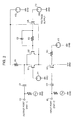
- FIG. 2 is a circuit diagram of the variable gain amplifier as shown in FIG. 1 .
- Amplifying unit 20 as shown in FIG. 1 is a cascade amplifier which includes common-emitter transistor Q 0 and common base transistor Q 1 .
- variable gain unit 30 as shown in FIG. 1 includes transistors Q 2 and Q 3 , resistor R 2 and capacitor C 2 .
- resistance R 0 for applying DC bias V 3 to the base of transistor Q 0 Resistor R 1 as a load resistance for the cascade amplifier, voltage supply V 1 for biasing the base of transistor Q 1 , voltage supply V 2 for the variable gain amplifier of the present invention as a whole, input port 10 , output terminal 40 , and power supplies and coupling capacitors connected with input port 10 and output port 40 .
- Resistance R 2 may be replaced by inductance L, and bipolar transistors may be replaced by other types such MOS transistors.
- the electrode for controlling the transistors are the bases of the bipolar transistors, or gates of the MOS transistors.
- Resistance R 2 gives a current feedback for transistor Q 2 , thereby lowering the mutual conductance “gm” of transistor Q 2 , and limiting the current flowing from voltage supply V 0 .
- the emitter area ratio (the emitter area of transistor Q 2 : the emitter area of Q 3 ) made to be 1: n where “n” is greater than or equal to 1, thereby controlling each current.
- Capacitor C 2 is connected in parallel with R 2 connected with the base of transistor Q 2 is a bypass capacitor for lowering the impedance of the base of transistor Q 2 in higher frequency range.
- Capacitor C 2 is a peaking capacitor, because it improves the high frequency characteristics.
- the current of the cascade amplifier by voltage V 2 flows through R 1 .
- the base of transistor Q 1 is biased by voltage supply V 1 , while transistor Q 2 is turned off. Therefore, the current flows through R 1 and Q 1 into transistor Q 0 .
- transistor Q 0 flows into the earth (GND) connected with the emitter of transistor Q 0 , because transistor Q 0 becomes a constant current DC current source due to the bias of its base. Therefore, when voltage Vo is lower than voltage V 1 , the signal inputted from PORTO is amplified with the gain of the cascade amplifier itself. On the other hand, when voltage V 0 is higher than voltage V 1 , transistors Q 2 and Q 3 are switched on, and the current by voltage V 2 flows these transistors, but does not flow through the transistors Q 1 and Q 0 . Therefore, the gain of the cascade amplifier including transistors Q 1 and Q 0 becomes low.
- transistor Q 3 is turned on by voltage V 0 , and the current by voltage V 2 flows into transistor Q 0 via transistor Q 3 . Further, the current through resistance R 1 by voltage V 2 flows also into transistor Q 0 via transistor Q 2 , because transistor Q 1 is turned off.
- the current through transistor Q 2 varies the gain of the cascade amplifier, because it depends upon the load current through load resistance R 1 of the cascade amplifier.
- the current through transistor Q 2 added to the current through Transistor Q 3 becomes the current through transistor Q 0 .
- the current through transistor Q 2 added to the current through transistor Q 3 flows via transistor Q 0 into the earth (GND) connected with the emitter of transistor Q 0 , because transistor Q 0 becomes a constant current DC current source due to the bias of its base. Therefore, when voltage V 0 is higher than voltage V 1 , the signal inputted from PORTO is amplified with the gain controlled by the variable gain unit including transistors Q 2 and Q 3 .
- the current through Q 2 is smaller than the current through Q 1 in order to obtain the higher gain when V 0 is lower than V 1 and to obtain the lower gain when V 0 is higher than V 1 .
- FIG. 3 is a graph of a frequency characteristic of the variable gain amplifier of the present invention as shown in FIG. 2 .
- the cut off frequency is about 4 GHz both at the high gain and at the low gain, as shown in FIG. 3, thereby broadening the frequency characteristics regardless of the amplification gain.
- the present invention is applicable to a low noise amplifier wherein an emitter of a common-emitter transistor is not connected with a resister, because the amplification gain is controlled by a base of a common-base transistor. Further, the present invention is applicable to a mixer, antenna switch.
- variable gain amplifier of the present invention is applicable to a dual band pocket telephone suc as GSM (global system for mobile communication), because 800 MHz and 1.9 GHz signals are received by using a single amplifier.
- GSM global system for mobile communication
Landscapes
- Control Of Amplification And Gain Control (AREA)
- Amplifiers (AREA)
- Networks Using Active Elements (AREA)
Abstract
Description
Claims (5)
Applications Claiming Priority (2)
| Application Number | Priority Date | Filing Date | Title |
|---|---|---|---|
| JP2000222705A JP2002043875A (en) | 2000-07-24 | 2000-07-24 | Variable gain amplifier and electronic equipment provided with the same |
| JP2000-222705 | 2000-07-24 |
Publications (2)
| Publication Number | Publication Date |
|---|---|
| US20020008582A1 US20020008582A1 (en) | 2002-01-24 |
| US6509798B2 true US6509798B2 (en) | 2003-01-21 |
Family
ID=18716914
Family Applications (1)
| Application Number | Title | Priority Date | Filing Date |
|---|---|---|---|
| US09/888,179 Expired - Fee Related US6509798B2 (en) | 2000-07-24 | 2001-06-22 | Variable gain amplifier |
Country Status (4)
| Country | Link |
|---|---|
| US (1) | US6509798B2 (en) |
| EP (1) | EP1176712A3 (en) |
| JP (1) | JP2002043875A (en) |
| KR (1) | KR100425757B1 (en) |
Cited By (3)
| Publication number | Priority date | Publication date | Assignee | Title |
|---|---|---|---|---|
| US20050017807A1 (en) * | 2003-07-21 | 2005-01-27 | Ying-Yao Lin | Linear-in-decibel variable gain amplifier |
| US20050046479A1 (en) * | 2003-09-01 | 2005-03-03 | Ying-Yao Lin | Linear-in-decibel variable gain amplifier |
| US20050073362A1 (en) * | 2003-10-01 | 2005-04-07 | Ying-Yao Lin | Linear decibel-scale variable gain amplifier |
Families Citing this family (7)
| Publication number | Priority date | Publication date | Assignee | Title |
|---|---|---|---|---|
| JP4405113B2 (en) * | 2001-08-16 | 2010-01-27 | パナソニック株式会社 | Variable gain amplifier circuit |
| KR100468355B1 (en) * | 2002-11-25 | 2005-01-27 | 인티그런트 테크놀로지즈(주) | Circuit for Controlling Slope and Offset of Gain Curve of Variable Gain Amplifier |
| KR100857223B1 (en) | 2007-02-28 | 2008-09-05 | 충북대학교 산학협력단 | Variable gain amplifier |
| US8633576B2 (en) | 2011-04-21 | 2014-01-21 | Tessera, Inc. | Stacked chip-on-board module with edge connector |
| KR101931256B1 (en) | 2012-07-25 | 2018-12-20 | 삼성전자주식회사 | Wireless power reception apparatus and method |
| CN103107789B (en) * | 2013-02-03 | 2015-12-02 | 北京工业大学 | The variable gain amplifier that a kind of common-mode feedback resistor shares |
| JP6702083B2 (en) * | 2016-08-23 | 2020-05-27 | 株式会社村田製作所 | High frequency amplifier module |
Citations (8)
| Publication number | Priority date | Publication date | Assignee | Title |
|---|---|---|---|---|
| US4344043A (en) * | 1980-04-23 | 1982-08-10 | Rca Corporation | Variable load impedance gain-controlled amplifier |
| JPH0474010A (en) | 1990-07-13 | 1992-03-09 | Iwatsu Electric Co Ltd | Differential amplifier |
| WO1995007574A1 (en) | 1993-09-04 | 1995-03-16 | Deutsche Thomson-Brandt Gmbh | Amplifier stage with a db-linear output voltage |
| US5999058A (en) * | 1997-02-21 | 1999-12-07 | Nec Corporation | Microwave amplifier |
| US6043710A (en) * | 1997-11-14 | 2000-03-28 | Mitel Semiconductor Limited | Low-voltage amplifiers |
| US6046641A (en) * | 1998-07-22 | 2000-04-04 | Eni Technologies, Inc. | Parallel HV MOSFET high power stable amplifier |
| US6181206B1 (en) * | 1998-06-23 | 2001-01-30 | Stmicroelectronics S.R.L. | Low noise RF amplifier with programmable gain |
| US6249153B1 (en) * | 1999-05-25 | 2001-06-19 | Micrel Incorporated | High slew rate input differential pair with common mode input to ground |
Family Cites Families (5)
| Publication number | Priority date | Publication date | Assignee | Title |
|---|---|---|---|---|
| DE2262089C3 (en) * | 1972-12-19 | 1975-10-30 | Philips Patentverwaltung Gmbh, 2000 Hamburg | Circuit arrangement for electronic frequency influencing, in particular electronic sound adjuster |
| BR9703233A (en) * | 1997-05-30 | 1998-12-29 | Brasilia Telecom | Improvement introduced in transimpedance amplifier |
| US6046640A (en) * | 1997-11-07 | 2000-04-04 | Analog Devices, Inc. | Switched-gain cascode amplifier using loading network for gain control |
| US6628170B2 (en) * | 1998-06-04 | 2003-09-30 | Analog Devices, Inc. | Low noise amplifier |
| US5999056A (en) * | 1998-06-30 | 1999-12-07 | Philips Electronics North Amercia Corporation | Variable gain amplifier using impedance network |
-
2000
- 2000-07-24 JP JP2000222705A patent/JP2002043875A/en not_active Withdrawn
-
2001
- 2001-04-27 KR KR10-2001-0022958A patent/KR100425757B1/en not_active Expired - Fee Related
- 2001-04-27 EP EP01110438A patent/EP1176712A3/en not_active Withdrawn
- 2001-06-22 US US09/888,179 patent/US6509798B2/en not_active Expired - Fee Related
Patent Citations (8)
| Publication number | Priority date | Publication date | Assignee | Title |
|---|---|---|---|---|
| US4344043A (en) * | 1980-04-23 | 1982-08-10 | Rca Corporation | Variable load impedance gain-controlled amplifier |
| JPH0474010A (en) | 1990-07-13 | 1992-03-09 | Iwatsu Electric Co Ltd | Differential amplifier |
| WO1995007574A1 (en) | 1993-09-04 | 1995-03-16 | Deutsche Thomson-Brandt Gmbh | Amplifier stage with a db-linear output voltage |
| US5999058A (en) * | 1997-02-21 | 1999-12-07 | Nec Corporation | Microwave amplifier |
| US6043710A (en) * | 1997-11-14 | 2000-03-28 | Mitel Semiconductor Limited | Low-voltage amplifiers |
| US6181206B1 (en) * | 1998-06-23 | 2001-01-30 | Stmicroelectronics S.R.L. | Low noise RF amplifier with programmable gain |
| US6046641A (en) * | 1998-07-22 | 2000-04-04 | Eni Technologies, Inc. | Parallel HV MOSFET high power stable amplifier |
| US6249153B1 (en) * | 1999-05-25 | 2001-06-19 | Micrel Incorporated | High slew rate input differential pair with common mode input to ground |
Cited By (6)
| Publication number | Priority date | Publication date | Assignee | Title |
|---|---|---|---|---|
| US20050017807A1 (en) * | 2003-07-21 | 2005-01-27 | Ying-Yao Lin | Linear-in-decibel variable gain amplifier |
| US7091786B2 (en) | 2003-07-21 | 2006-08-15 | Realtek Semiconductor Corp. | Linear-in-decibel variable gain amplifier |
| US20050046479A1 (en) * | 2003-09-01 | 2005-03-03 | Ying-Yao Lin | Linear-in-decibel variable gain amplifier |
| US7075368B2 (en) | 2003-09-01 | 2006-07-11 | Realtek Semiconductor Corp. | Linear-in-decibel variable gain amplifier |
| US20050073362A1 (en) * | 2003-10-01 | 2005-04-07 | Ying-Yao Lin | Linear decibel-scale variable gain amplifier |
| US7078972B2 (en) | 2003-10-01 | 2006-07-18 | Realtek Semiconductor Corp. | Linear decibel-scale variable gain amplifier |
Also Published As
| Publication number | Publication date |
|---|---|
| JP2002043875A (en) | 2002-02-08 |
| KR20020008746A (en) | 2002-01-31 |
| EP1176712A3 (en) | 2003-12-17 |
| EP1176712A2 (en) | 2002-01-30 |
| KR100425757B1 (en) | 2004-04-03 |
| US20020008582A1 (en) | 2002-01-24 |
Similar Documents
| Publication | Publication Date | Title |
|---|---|---|
| KR100704568B1 (en) | Variable gain low noise amplifier | |
| US6724259B2 (en) | Variable gain amplifier | |
| KR102287445B1 (en) | System and method for bypassing a low noise amplifier | |
| US6778016B2 (en) | Simple self-biased cascode amplifier circuit | |
| CN101515784B (en) | Amplifier, attenuation module and method for attenuating radio frequency signals | |
| KR20020038498A (en) | High frequency power amplifier, wireless communication apparatus and wireless communication system | |
| KR20030011233A (en) | High frequency power amplifier circuit device | |
| KR20050027993A (en) | Switchable gain amplifier | |
| US5844443A (en) | Linear high-frequency amplifier with high input impedance and high power efficiency | |
| JP4405113B2 (en) | Variable gain amplifier circuit | |
| US6509798B2 (en) | Variable gain amplifier | |
| JP5064224B2 (en) | Dual bias control circuit | |
| US6919761B2 (en) | Wideband variable gain amplifier with high linearity operating in switch mode | |
| US7400192B2 (en) | Low noise amplifier and differential amplifier with variable gain mode | |
| CN1619950B (en) | Variable amplifier and mobile wireless terminal using same | |
| US8115552B2 (en) | Amplifier circuit with step gain | |
| US6100763A (en) | Circuit for RF buffer and method of operation | |
| JP2020188292A (en) | Power amplifier circuit and bias control circuit | |
| US20030058045A1 (en) | Power control in RF amplifiers | |
| US7541876B2 (en) | Amplifier and method for operating the same | |
| US20260045917A1 (en) | Amplifier circuit | |
| US9407220B1 (en) | Digitally controlled variable transductance stage for microwave mixers and amplifiers | |
| JPH0548348A (en) | Power amplifier circuit | |
| JPH10126215A (en) | Variable damping device | |
| KR101045541B1 (en) | Mixer with Current Mirroring |
Legal Events
| Date | Code | Title | Description |
|---|---|---|---|
| AS | Assignment |
Owner name: NEC CORPORATION, JAPAN Free format text: ASSIGNMENT OF ASSIGNORS INTEREST;ASSIGNOR:KURODA, HIDEHIKO;REEL/FRAME:011951/0926 Effective date: 20010402 |
|
| FEPP | Fee payment procedure |
Free format text: PAYOR NUMBER ASSIGNED (ORIGINAL EVENT CODE: ASPN); ENTITY STATUS OF PATENT OWNER: LARGE ENTITY |
|
| AS | Assignment |
Owner name: NEC COMPOUND SEMICONDUCTOR DEVICES, LTD., JAPAN Free format text: ASSIGNMENT OF ASSIGNORS INTEREST;ASSIGNOR:NEC CORPORATION;REEL/FRAME:013507/0994 Effective date: 20021016 |
|
| AS | Assignment |
Owner name: NEC ELECTRONICS CORPORATION, JAPAN Free format text: ASSIGNMENT OF ASSIGNORS INTEREST;ASSIGNOR:NEC COMPOUND SEMICONDUCTOR DEVICES, LTD.;REEL/FRAME:017422/0528 Effective date: 20060315 |
|
| FPAY | Fee payment |
Year of fee payment: 4 |
|
| FPAY | Fee payment |
Year of fee payment: 8 |
|
| AS | Assignment |
Owner name: RENESAS ELECTRONICS CORPORATION, JAPAN Free format text: CHANGE OF NAME;ASSIGNOR:NEC ELECTRONICS CORPORATION;REEL/FRAME:025486/0443 Effective date: 20100401 |
|
| REMI | Maintenance fee reminder mailed | ||
| LAPS | Lapse for failure to pay maintenance fees | ||
| STCH | Information on status: patent discontinuation |
Free format text: PATENT EXPIRED DUE TO NONPAYMENT OF MAINTENANCE FEES UNDER 37 CFR 1.362 |
|
| STCH | Information on status: patent discontinuation |
Free format text: PATENT EXPIRED DUE TO NONPAYMENT OF MAINTENANCE FEES UNDER 37 CFR 1.362 |
|
| FP | Lapsed due to failure to pay maintenance fee |
Effective date: 20150121 |