US6509607B1 - Semiconductor device with reduced source diffusion distance and method of making same - Google Patents
Semiconductor device with reduced source diffusion distance and method of making same Download PDFInfo
- Publication number
- US6509607B1 US6509607B1 US09/505,808 US50580800A US6509607B1 US 6509607 B1 US6509607 B1 US 6509607B1 US 50580800 A US50580800 A US 50580800A US 6509607 B1 US6509607 B1 US 6509607B1
- Authority
- US
- United States
- Prior art keywords
- region
- source
- indentation
- portions
- side walls
- Prior art date
- Legal status (The legal status is an assumption and is not a legal conclusion. Google has not performed a legal analysis and makes no representation as to the accuracy of the status listed.)
- Expired - Lifetime
Links
Images


Classifications
-
- H—ELECTRICITY
- H10—SEMICONDUCTOR DEVICES; ELECTRIC SOLID-STATE DEVICES NOT OTHERWISE PROVIDED FOR
- H10D—INORGANIC ELECTRIC SEMICONDUCTOR DEVICES
- H10D30/00—Field-effect transistors [FET]
- H10D30/60—Insulated-gate field-effect transistors [IGFET]
- H10D30/64—Double-diffused metal-oxide semiconductor [DMOS] FETs
- H10D30/66—Vertical DMOS [VDMOS] FETs
- H10D30/668—Vertical DMOS [VDMOS] FETs having trench gate electrodes, e.g. UMOS transistors
-
- H—ELECTRICITY
- H10—SEMICONDUCTOR DEVICES; ELECTRIC SOLID-STATE DEVICES NOT OTHERWISE PROVIDED FOR
- H10D—INORGANIC ELECTRIC SEMICONDUCTOR DEVICES
- H10D12/00—Bipolar devices controlled by the field effect, e.g. insulated-gate bipolar transistors [IGBT]
- H10D12/01—Manufacture or treatment
- H10D12/031—Manufacture or treatment of IGBTs
- H10D12/032—Manufacture or treatment of IGBTs of vertical IGBTs
- H10D12/035—Etching a recess in the emitter region
-
- H—ELECTRICITY
- H10—SEMICONDUCTOR DEVICES; ELECTRIC SOLID-STATE DEVICES NOT OTHERWISE PROVIDED FOR
- H10D—INORGANIC ELECTRIC SEMICONDUCTOR DEVICES
- H10D12/00—Bipolar devices controlled by the field effect, e.g. insulated-gate bipolar transistors [IGBT]
- H10D12/411—Insulated-gate bipolar transistors [IGBT]
- H10D12/441—Vertical IGBTs
- H10D12/461—Vertical IGBTs having non-planar surfaces, e.g. having trenches, recesses or pillars in the surfaces of the emitter, base or collector regions
- H10D12/481—Vertical IGBTs having non-planar surfaces, e.g. having trenches, recesses or pillars in the surfaces of the emitter, base or collector regions having gate structures on slanted surfaces, on vertical surfaces, or in grooves, e.g. trench gate IGBTs
-
- H—ELECTRICITY
- H10—SEMICONDUCTOR DEVICES; ELECTRIC SOLID-STATE DEVICES NOT OTHERWISE PROVIDED FOR
- H10D—INORGANIC ELECTRIC SEMICONDUCTOR DEVICES
- H10D62/00—Semiconductor bodies, or regions thereof, of devices having potential barriers
- H10D62/10—Shapes, relative sizes or dispositions of the regions of the semiconductor bodies; Shapes of the semiconductor bodies
- H10D62/17—Semiconductor regions connected to electrodes not carrying current to be rectified, amplified or switched, e.g. channel regions
- H10D62/393—Body regions of DMOS transistors or IGBTs
-
- H—ELECTRICITY
- H10—SEMICONDUCTOR DEVICES; ELECTRIC SOLID-STATE DEVICES NOT OTHERWISE PROVIDED FOR
- H10D—INORGANIC ELECTRIC SEMICONDUCTOR DEVICES
- H10D64/00—Electrodes of devices having potential barriers
- H10D64/20—Electrodes characterised by their shapes, relative sizes or dispositions
- H10D64/23—Electrodes carrying the current to be rectified, amplified, oscillated or switched, e.g. sources, drains, anodes or cathodes
- H10D64/251—Source or drain electrodes for field-effect devices
- H10D64/252—Source or drain electrodes for field-effect devices for vertical or pseudo-vertical devices
- H10D64/2527—Source or drain electrodes for field-effect devices for vertical or pseudo-vertical devices for vertical devices wherein the source or drain electrodes are recessed in semiconductor bodies
-
- H—ELECTRICITY
- H10—SEMICONDUCTOR DEVICES; ELECTRIC SOLID-STATE DEVICES NOT OTHERWISE PROVIDED FOR
- H10D—INORGANIC ELECTRIC SEMICONDUCTOR DEVICES
- H10D64/00—Electrodes of devices having potential barriers
- H10D64/20—Electrodes characterised by their shapes, relative sizes or dispositions
- H10D64/23—Electrodes carrying the current to be rectified, amplified, oscillated or switched, e.g. sources, drains, anodes or cathodes
- H10D64/251—Source or drain electrodes for field-effect devices
- H10D64/256—Source or drain electrodes for field-effect devices for lateral devices wherein the source or drain electrodes are recessed in semiconductor bodies
Definitions
- the present invention relates to a semiconductor device and in particular to a semiconductor device having a structure suitable for the formation of a vertical channel MOS power transistor.
- FIG. 1 of the U.S. patent illustrates an early structure in which in an on-state a field from a gate forms a horizontal conducting chattel, allowing current to flow laterally beneath the gate. After flowing laterally, the current must then flow vertically to reach a drain region.
- FIG. 2 of the above US patent illustrates an alternative structure generally referred to as a UMOS structure. In that structure, source, body and drain regions are arranged vertically adjacent a trench fondled in a wafer surface, the trench being generally of U-shaped cross-section. Current thus flows more efficiently in the vertical direction only.
- the structure of FIG. 1 of the U.S. patent illustrates an early structure in which in an on-state a field from a gate forms a horizontal conducting chattel, allowing current to flow laterally beneath the gate. After flowing laterally, the current must then flow vertically to reach a drain region.
- FIG. 2 of the above US patent illustrates an alternative structure generally referred to as a UMOS structure. In that structure, source, body and drain regions
- FIG. 3 of the above US patent seeks to provide a UMOS structure which is not subject to these disadvantages by providing a vertical gate in a structure with a planar surface whilst still enabling contact to be made to the gate which is embedded beneath that surface.
- a drain region is overlaid by a body region which defines a substantially planar upper surface.
- Source regions extend from the upper surface towards the drain region and a series of indentations extend from the upper surface of the body region.
- the indentations are arranged such that lower side walls of each indentation are defined by portions of the drain and body regions and upper side walls of each indentation are defined by source regions.
- a lower portion of each indentation is filled with a gate region isolated from the side walls of the indentation by a first insulating layer and covered by a second insulating layer. The indentations are completely filled with the material malting up the gate region and the first and second insulating layers.
- a source conductor overlies the upper surface of the body region to contact portions of the source regions which are substantially coplanar with the upper surface of the body region.
- a semiconductor device comprising a drain region, a body region overlying the drain region and defining an upper surface, source regions extending from adjacent the upper surface of the body region towards the drain region, and a series of indentations extending into the body region such that lower side walls of each indentation are defined by portions of the drain and body regions and upper side walls of each indentation are defined by the source regions, wherein a lower portion of each indentation is filled with a gate region isolated from the side walls by a first insulating layer and covered by a second insulating layer, a source conductor overlies the upper surface and is electrically connected to the source and body regions, and a gate conductor is electrically connected to each gate region, the source conductor extending into an upper portion of each indentation to contact portions of the upper side walls of the indentation which are defined by the source regions.
- the upper surface of the body region is substantially planar and the source regions define upper surfaces which are substantially coplanar with the upper surface of the body region, the source conductor overlying and electrically contacting the upper surfaces of the source regions.
- FIG. 4 is a schematic illustration of the cross-section of FIG. 3 after trenches have been etched into the semiconductor body
- FIG. 5 is a schematic illustration of the cross-section of FIG. 4 after the trenches have been coated with oxide material
- FIG. 6 is a schematic illustration of the cross-section of FIG. 5 after the trenches have been partially filled with polysilicon
- FIG. 7 is a schematic illustration of the cross-section of FIG. 6 after the semiconductor body has been doped with p-type dopant
- FIG. 8 is a schematic illustration of the cross-section of FIG. 7 after deposition of an isolation layer
- FIG. 9 is a schematic illustration of the cross-section of FIG. 8 after deposition of a planarising layer of photo-resist
- FIG. 10 is a schematic illustration of the cross-section of FIG. 9 after partially etching back the upper surface
- FIG. 11 is a schematic illustration of the cross-section of FIG. 10 after a further etch-back.
- FIG. 12 is a schematic illustration of the cross-section of FIG. 1 after deposition of a source conductor to form an n-channel (n-p-n) UMOS device according to the invention.
- the illustrated prior art structure comprises a series of trenches which form indentations extending in a direction perpendicular to the plane of FIG. 1 .
- Each trench structure overlies an n+ type semiconductor drain region 1 , an n ⁇ type drain region 2 , and a p-type body region 3 .
- Each trench structure comprises n+ source regions 4 , a gate region 5 isolated from the body and source regions by a first insulating layer 6 , and a second insulating layer 7 .
- the insulating layer 6 extends only to the top of the gate region 5 , but it will be appreciated that the layer 6 may extend to the top of the layer 7 .
- a source-contacting conductor 8 extends over the substantially planar surface defined by the upper surfaces of the body region 3 , source reunions 4 and insulating layers 7 .
- each gate region 5 and adjacent insulating layers 6 and 7 completely fill an indentation formed in the semiconductor structure, the side walls of the indentation corresponding in position to the boundary between the first insulating layer 6 and the drain region 2 , the body region 3 and source regions 4 , and the boundary between the second insulating layer 7 and source regions 4 .
- the illustrated device can be turned on to cause current to flow between the source regions 4 and the drain region 1 by applying appropriate potentials to the source, drain and gate so as to establish a conducting channel region through the body region 3 adjacent the gate region 5 .
- the operational characteristics of the structure are entirely conventional and will not be further described herein.
- the minimum spacing between the indentations of adjacent trench structures is the sum of the spacing between adjacent source regions 4 (indicated by arrow 9 in FIG. 1) and twice ale width of the source regions 4 (indicated by arrow 10 in FIG. 1 ).
- the inter-source spacing must be sufficient to ensure adequate inhibition to n-p-n bipolar turn-on, and typically is 1 ⁇ m.
- the source width must be sufficient to carry an adequate current to the source regions and typically is also 1 ⁇ m. Thus a minimum inter-indentation spacing is typically 3 ⁇ m.
- FIG. 2 this shows an embodiment of the present invention.
- the same numerals are used for equivalent structures in FIGS. 1 and 2.
- the difference between the two illustrated structures is that in FIG. 1 the upper surface of the insulating layer 7 is coplanar with the coplanar upper surfaces of the body region 3 and source regions 4 and is therefore coplanar with the lower surface of the source conductor 8 , whereas in the arrangement of FIG. 2 the upper surface of the insulating layer 7 is recessed such that the conductor layer 8 penetrates into the upper portion of the indentations to a depth indicated by arrow 11 .
- the contact area between the conductor layer 8 and each source region 4 is a function of the sum of the dimensions indicated by arrows 10 and 11 . Accordingly, for a dimension 11 of 0.6 ⁇ m, the dimensions 10 can be relatively small, for example 0.4 ⁇ m rather than 1 ⁇ m, resulting in a minimum spacing between adjacent indentations of 1.8 ⁇ m rather than 3 ⁇ m.
- an unpatterned p+ surface dopant concentration enhancement region 12 may be introduced orthogonal to the upper surface of the body region 3 and source regions 4 without increasing the source contact resistance to an unacceptable extent given that the source conductor 8 contacts the sources 4 via the side walls of the indentations above the upper surface of the insulating layer 7 .
- the surface dopant concentration enhancement region does not penetrate to a significant extent into the side walls of the indentations defined by the source regions 4 .
- a semiconductor body is formed on a substrate defining an n+ type semiconductor drain region 13 .
- the semiconductor body comprises an n ⁇ type drain region 14 , extending to an upper surface 15 , which supports a masking layer 16 which may be selectively removed by etching to define areas where trenches are to be formed in the region 14 .
- the drain region 14 may be an epitaxial layer.
- the masking layer 16 may comprise a single material type, for example silicon dioxide, or it may be a multi-layer comprising several different materials, for example silicon dioxide/silicon nitride/silicon dioxide.
- trenches are etched to a predetermined depth through the exposed surface 15 and into region 14 , as shown in FIG. 4, using a known method, for example reactive ion etching.
- the illustrated multi-layer structure will be formed on a wafer substrate which might be 600 ⁇ m thick.
- the substrate in effect foils the drain region 13 of FIG. 3 .
- the layers 14 and 16 built up on the substrate will be very much thinner than the substrate itself.
- the region 14 may be 6 ⁇ m thick.
- the layer 13 is shown in the Figures as being relatively thin simply for the purposes of illustration.
- An insulating oxide layer 17 is formed on the trench walls using a know technique as shown in FIG. 5 .
- a know technique is thermal oxidation.
- Layer 17 may also be formed as a composite oxide/nitride layer.
- a gate material 18 such as polysilicon is introduced into the trenches, for example using a low pressure chemical vapour deposition technique.
- the polysilicon gate material 18 is arranged to partially fill the trenches, as shown in FIG. 6, for example by first filling the trenches and then etching back some of the polysilicon 18 .
- the polysilicon 18 may be doped to effect an improvement in conductivity. This may be done during or after deposition.
- aluminium gates may be arranged partially to fill the trenches, without requiring to be etched back, using a method described in WO 9700536.
- p-type body dopant is introduced laterally into region 14 through the side walls of the trenches, and is then diffused to form p-type body regions 19 .
- the body dopant may be introduced into the trench side walls using charged dopant ions (for example ionic boron) which pass directly through the oxide layer 17 and into the region 14 .
- dopant ions for example ionic boron
- other known methods of dopant introduction may be used, for example gaseous predeposition. Some methods may require that the oxide layer 17 is first removed from the walls of the trenches above the gate material.
- FIG. 7 however illustrates a method in which the layer 17 remains intact.
- the portion of the layer 17 above the gate region 18 is removed, and then source dopant is introduced laterally through the side walls of the trenches, using a technique such as one of those described above, to form source regions 20 .
- the source dopant is prevented from entering at least pail of the upper surface of the substrate by those portions of the trench masking layer 16 which have not been removed. It will be appreciated that although in the method described above the portions of the latter 17 above the gate region 18 are removed before source dopant introduction, dopant could be implanted through the layer 17 above the gate region 18 .
- the diffusion of the source dopant is arranged such that it penetrates to a lesser distance than the body dopant, so that a portion of body region 19 is interposed between each source region 20 and drain region 14 .
- the penetration distance of the source dopant must be closely controlled in order that the resultant channel width (that is the position of the boundary between the regions 19 and 20 relative to the position of the upper surface of each gate region 18 ) is accurately determined. It will be appreciated that driving in the source regions 20 will cause some further diffusion of the dopant forming the body regions 19 , and that this further diffusion must also be taken into account when determining the desired relative positions of the source and body region boundaries.
- the present invention allows for a minimal source diffusion distance, by eliminating the requirement for a wide lateral source contact width at the surface 15 , such a wide lateral source contact being required in prior art devices in which the only contact with a source conductor is at the surface 15 . Consequently, the vertical thickness of the portion of body region 19 interposed between a source region 20 and the drain region 14 , known as the channel width, is more accurately determined.
- An isolation material 21 such as TEOS- or silane-based silicon dioxide is then deposited on the structure.
- the top surface of this layer 21 may then be planarised, using for example a layer 22 of photoresist, as shown in FIG. 9 .
- the layer of photoresist 22 is spun onto the wafer and then balled to leave a substantially flat top surface.
- the structure of FIG. 9 is then subjected to a partial etch-back using an etch with 1:1 selectivity between layers 21 and 22 , which leaves a new top surface of layer 21 substantially flat as shown in FIG. 10.
- a second etch-back is then carried out, this time with 1:1 selectivity between layer 21 and 16 , to arrive at the intermediate structure of FIG. 11 .
- the etch-back which results in the structure of FIG. 11 will have a high selectivity between layers 21 and 16 (both for example of silicon dioxide) and regions 19 and 20 (both silicon).
- layers 21 and 16 both for example of silicon dioxide
- regions 19 and 20 both silicon.
- the layer 16 is completely removed, exposing the substantially planar silicon surface below, and the layer 21 is substantially recessed below that planar surface.
- a shallow p-type implant may additionally be carried out at this point, in order to boost the surface dopant concentration of p-type regions 19 (such an implant is not shown in FIG. 11 ).
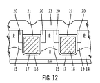
- a layer of metal 23 is then added to the upper surface of the structure, to form an electrical contact to the source regions 20 and body regions 19 , as shown in FIG. 12 .
- the gate regions 18 will be connected elsewhere to a gate contact metallisation region.
- a p-type body region is present in the structure in the form of a layer of uniform thickness before the trenches are etched, that is at the stage shown in FIG. 3, This p-type body region would therefore be present at each of the stages shown in FIGS. 3, 4 , 5 and 6 . Lateral introduction of p-type dopant through the trench side walls is not then necessary at the stage shown by FIG. 7 .
- the cross-sections at each of the stages shown in FIGS. 8, 9 , 10 , 11 and 12 would show a straight horizontal rather than curved boundary between layers 19 and 14 between the trenches.
- the completed structure would have the cross-section shown in FIG. 2 rather than that shown in FIG. 12 .
- p and n type regions may be interchanged throughout to arrive at a p-channel (p-n-p) rather than n-channel (n-p-n) structure.
- FIGS. 3 to 12 illustrate the formation of a device comprising two adjacent parallel trenches. It will be appreciated that the present invention may be used with a wide variety of trench configurations, for example the formation of a hexagonal array in which trenches are etched in spaces defined between a tightly packed array of hexagonal mesa areas on the surface of a substrate, or an array in which trenches are etched in spaces defined between regularly spaced square mesa areas arranged in rows with the mesa areas of adjacent rows offset by half the pitch of mesa areas in each row.
Landscapes
- Insulated Gate Type Field-Effect Transistor (AREA)
- Electrodes Of Semiconductors (AREA)
Abstract
Description
Claims (14)
Applications Claiming Priority (2)
| Application Number | Priority Date | Filing Date | Title |
|---|---|---|---|
| GB9903594A GB2347014B (en) | 1999-02-18 | 1999-02-18 | Semiconductor device |
| GB9903594 | 1999-02-18 |
Publications (1)
| Publication Number | Publication Date |
|---|---|
| US6509607B1 true US6509607B1 (en) | 2003-01-21 |
Family
ID=10847934
Family Applications (1)
| Application Number | Title | Priority Date | Filing Date |
|---|---|---|---|
| US09/505,808 Expired - Lifetime US6509607B1 (en) | 1999-02-18 | 2000-02-17 | Semiconductor device with reduced source diffusion distance and method of making same |
Country Status (2)
| Country | Link |
|---|---|
| US (1) | US6509607B1 (en) |
| GB (1) | GB2347014B (en) |
Cited By (12)
| Publication number | Priority date | Publication date | Assignee | Title |
|---|---|---|---|---|
| US6573559B2 (en) * | 2000-03-01 | 2003-06-03 | Shindengen Electric Manufacturing Co., Ltd. | Transistor and method of manufacturing the same |
| US20030160262A1 (en) * | 2002-02-20 | 2003-08-28 | Mizue Kitada | Diode device and transistor device |
| US6690061B2 (en) * | 2001-09-26 | 2004-02-10 | Kabushiki Kaisha Toshiba | MOS Semiconductor device |
| US20040082142A1 (en) * | 2002-09-13 | 2004-04-29 | Jana Hansel | Fabrication method for a semiconductor structure having a partly filled trench |
| US20050224868A1 (en) * | 1999-03-01 | 2005-10-13 | Kocon Christopher B | MOS-gated device having a buried gate and process for forming same |
| US20080085591A1 (en) * | 2006-10-06 | 2008-04-10 | Gomez Mercedes P | Novel Gate Structure with Low Resistance for High Power Semiconductor Devices |
| US20090273026A1 (en) * | 2002-10-03 | 2009-11-05 | Wilson Peter H | Trench-gate ldmos structures |
| US20120018793A1 (en) * | 2007-04-30 | 2012-01-26 | Anup Bhalla | Device structure and manufacturing method using HDP deposited using deposited source-body implant block |
| JP2014033223A (en) * | 2013-10-15 | 2014-02-20 | Fuji Electric Co Ltd | Silicon carbide semiconductor device and method of manufacturing the same |
| KR20170080975A (en) * | 2015-12-31 | 2017-07-11 | 매그나칩 반도체 유한회사 | Method for fabricating of Cell pitch reduced Semiconductor Device and Semiconductor Device |
| US11101373B2 (en) * | 2018-11-12 | 2021-08-24 | Denso Corporation | Insulated gate bipolar transistor and manufacturing method thereof |
| CN115881790A (en) * | 2023-03-08 | 2023-03-31 | 杭州朋声科技有限公司 | Contact self-aligned trench gate power device, manufacturing method and chip |
Families Citing this family (4)
| Publication number | Priority date | Publication date | Assignee | Title |
|---|---|---|---|---|
| JP2001085685A (en) * | 1999-09-13 | 2001-03-30 | Shindengen Electric Mfg Co Ltd | Transistor |
| JP4754353B2 (en) * | 2003-12-22 | 2011-08-24 | パナソニック株式会社 | Vertical trench gate semiconductor device and manufacturing method thereof |
| GB0404751D0 (en) * | 2004-03-03 | 2004-04-07 | Koninkl Philips Electronics Nv | Trench field effect transistor and method of making it |
| JP7468413B2 (en) | 2021-03-15 | 2024-04-16 | 三菱電機株式会社 | Semiconductor Device |
Citations (13)
| Publication number | Priority date | Publication date | Assignee | Title |
|---|---|---|---|---|
| US4364074A (en) | 1980-06-12 | 1982-12-14 | International Business Machines Corporation | V-MOS Device with self-aligned multiple electrodes |
| US4523369A (en) * | 1982-03-31 | 1985-06-18 | Tokyo Shibaura Denki Kabushiki Kaisha | Method for manufacturing a semiconductor device |
| US4929987A (en) | 1988-02-01 | 1990-05-29 | General Instrument Corporation | Method for setting the threshold voltage of a power mosfet |
| US4983535A (en) | 1981-10-15 | 1991-01-08 | Siliconix Incorporated | Vertical DMOS transistor fabrication process |
| US5086007A (en) | 1989-05-24 | 1992-02-04 | Fuji Electric Co., Ltd. | Method of manufacturing an insulated gate field effect transistor |
| US5576245A (en) | 1987-10-08 | 1996-11-19 | Siliconix Incorporated | Method of making vertical current flow field effect transistor |
| US5629543A (en) * | 1995-08-21 | 1997-05-13 | Siliconix Incorporated | Trenched DMOS transistor with buried layer for reduced on-resistance and ruggedness |
| US5656842A (en) | 1995-06-20 | 1997-08-12 | Mitsubishi Denki Kabushiki Kaisha | Vertical mosfet including a back gate electrode |
| US5691555A (en) * | 1993-05-19 | 1997-11-25 | Consorzio Per La Ricerca Sulla Microelettronica Nel Mezzogiorno | Integrated structure current sensing resistor for power devices particularly for overload self-protected power MOS devices |
| US5701026A (en) | 1994-10-25 | 1997-12-23 | Fuji Electric Co., Ltd. | Lateral trench MISFET |
| US5723891A (en) * | 1992-05-18 | 1998-03-03 | Texas Instruments Incorporated | Top-drain trench based resurf DMOS transistor structure |
| US5801408A (en) * | 1995-07-21 | 1998-09-01 | Mitsubishi Denki Kabushiki Kaisha | Insulated gate semiconductor device and method of manufacturing the same |
| US6084264A (en) * | 1998-11-25 | 2000-07-04 | Siliconix Incorporated | Trench MOSFET having improved breakdown and on-resistance characteristics |
-
1999
- 1999-02-18 GB GB9903594A patent/GB2347014B/en not_active Expired - Lifetime
-
2000
- 2000-02-17 US US09/505,808 patent/US6509607B1/en not_active Expired - Lifetime
Patent Citations (13)
| Publication number | Priority date | Publication date | Assignee | Title |
|---|---|---|---|---|
| US4364074A (en) | 1980-06-12 | 1982-12-14 | International Business Machines Corporation | V-MOS Device with self-aligned multiple electrodes |
| US4983535A (en) | 1981-10-15 | 1991-01-08 | Siliconix Incorporated | Vertical DMOS transistor fabrication process |
| US4523369A (en) * | 1982-03-31 | 1985-06-18 | Tokyo Shibaura Denki Kabushiki Kaisha | Method for manufacturing a semiconductor device |
| US5576245A (en) | 1987-10-08 | 1996-11-19 | Siliconix Incorporated | Method of making vertical current flow field effect transistor |
| US4929987A (en) | 1988-02-01 | 1990-05-29 | General Instrument Corporation | Method for setting the threshold voltage of a power mosfet |
| US5086007A (en) | 1989-05-24 | 1992-02-04 | Fuji Electric Co., Ltd. | Method of manufacturing an insulated gate field effect transistor |
| US5723891A (en) * | 1992-05-18 | 1998-03-03 | Texas Instruments Incorporated | Top-drain trench based resurf DMOS transistor structure |
| US5691555A (en) * | 1993-05-19 | 1997-11-25 | Consorzio Per La Ricerca Sulla Microelettronica Nel Mezzogiorno | Integrated structure current sensing resistor for power devices particularly for overload self-protected power MOS devices |
| US5701026A (en) | 1994-10-25 | 1997-12-23 | Fuji Electric Co., Ltd. | Lateral trench MISFET |
| US5656842A (en) | 1995-06-20 | 1997-08-12 | Mitsubishi Denki Kabushiki Kaisha | Vertical mosfet including a back gate electrode |
| US5801408A (en) * | 1995-07-21 | 1998-09-01 | Mitsubishi Denki Kabushiki Kaisha | Insulated gate semiconductor device and method of manufacturing the same |
| US5629543A (en) * | 1995-08-21 | 1997-05-13 | Siliconix Incorporated | Trenched DMOS transistor with buried layer for reduced on-resistance and ruggedness |
| US6084264A (en) * | 1998-11-25 | 2000-07-04 | Siliconix Incorporated | Trench MOSFET having improved breakdown and on-resistance characteristics |
Cited By (20)
| Publication number | Priority date | Publication date | Assignee | Title |
|---|---|---|---|---|
| US20050224868A1 (en) * | 1999-03-01 | 2005-10-13 | Kocon Christopher B | MOS-gated device having a buried gate and process for forming same |
| US7388254B2 (en) * | 1999-03-01 | 2008-06-17 | Fairchild Semiconductor Corporation | MOS-gated device having a buried gate and process for forming same |
| US6573559B2 (en) * | 2000-03-01 | 2003-06-03 | Shindengen Electric Manufacturing Co., Ltd. | Transistor and method of manufacturing the same |
| US6690061B2 (en) * | 2001-09-26 | 2004-02-10 | Kabushiki Kaisha Toshiba | MOS Semiconductor device |
| USRE47292E1 (en) * | 2001-09-26 | 2019-03-12 | Kabushiki Kaisha Toshiba | MOS semiconductor device |
| US20030160262A1 (en) * | 2002-02-20 | 2003-08-28 | Mizue Kitada | Diode device and transistor device |
| US7135718B2 (en) * | 2002-02-20 | 2006-11-14 | Shindengen Electric Manufacturing Co., Ltd. | Diode device and transistor device |
| US20040082142A1 (en) * | 2002-09-13 | 2004-04-29 | Jana Hansel | Fabrication method for a semiconductor structure having a partly filled trench |
| US6867137B2 (en) * | 2002-09-13 | 2005-03-15 | Infineon Technologies Ag | Fabrication method for a semiconductor structure having a partly filled trench |
| US20090273026A1 (en) * | 2002-10-03 | 2009-11-05 | Wilson Peter H | Trench-gate ldmos structures |
| US8198677B2 (en) * | 2002-10-03 | 2012-06-12 | Fairchild Semiconductor Corporation | Trench-gate LDMOS structures |
| US7589377B2 (en) * | 2006-10-06 | 2009-09-15 | The Boeing Company | Gate structure with low resistance for high power semiconductor devices |
| US20080085591A1 (en) * | 2006-10-06 | 2008-04-10 | Gomez Mercedes P | Novel Gate Structure with Low Resistance for High Power Semiconductor Devices |
| US20120018793A1 (en) * | 2007-04-30 | 2012-01-26 | Anup Bhalla | Device structure and manufacturing method using HDP deposited using deposited source-body implant block |
| US8372708B2 (en) * | 2007-04-30 | 2013-02-12 | Anup Bhalla | Device structure and manufacturing method using HDP deposited using deposited source-body implant block |
| JP2014033223A (en) * | 2013-10-15 | 2014-02-20 | Fuji Electric Co Ltd | Silicon carbide semiconductor device and method of manufacturing the same |
| KR20170080975A (en) * | 2015-12-31 | 2017-07-11 | 매그나칩 반도체 유한회사 | Method for fabricating of Cell pitch reduced Semiconductor Device and Semiconductor Device |
| US10038056B2 (en) * | 2015-12-31 | 2018-07-31 | Magnachip Semiconductor, Ltd. | Method for fabricating of cell pitch reduced semiconductor device and semiconductor device |
| US11101373B2 (en) * | 2018-11-12 | 2021-08-24 | Denso Corporation | Insulated gate bipolar transistor and manufacturing method thereof |
| CN115881790A (en) * | 2023-03-08 | 2023-03-31 | 杭州朋声科技有限公司 | Contact self-aligned trench gate power device, manufacturing method and chip |
Also Published As
| Publication number | Publication date |
|---|---|
| GB2347014B (en) | 2003-04-16 |
| GB2347014A (en) | 2000-08-23 |
| GB9903594D0 (en) | 1999-04-07 |
Similar Documents
| Publication | Publication Date | Title |
|---|---|---|
| US6376314B1 (en) | Method of semiconductor device fabrication | |
| US6498071B2 (en) | Manufacture of trench-gate semiconductor devices | |
| US6916745B2 (en) | Structure and method for forming a trench MOSFET having self-aligned features | |
| US6368921B1 (en) | Manufacture of trench-gate semiconductor devices | |
| EP1393362B1 (en) | Method of manufacturing a trench-gate semiconductor device | |
| US4803176A (en) | Integrated circuit structure with active device in merged slot and method of making same | |
| US6586800B2 (en) | Trench-gate semiconductor devices | |
| US6509607B1 (en) | Semiconductor device with reduced source diffusion distance and method of making same | |
| US20020140027A1 (en) | Field effect transistor and method of its manufacture | |
| JP2000252468A (en) | MOS gate device having buried gate and method of manufacturing the same | |
| US5721148A (en) | Method for manufacturing MOS type semiconductor device | |
| US6087224A (en) | Manufacture of trench-gate semiconductor devices | |
| US6521498B2 (en) | Manufacture or trench-gate semiconductor devices | |
| US6570218B1 (en) | MOSFET with a buried gate | |
| CN113964038A (en) | Manufacturing method of trench gate MOSFET device | |
| JP2002026323A (en) | Method of manufacturing trench gate type MIS device having thick polysilicon insulating layer at bottom of trench | |
| US20010023957A1 (en) | Trench-gate semiconductor devices | |
| KR100538602B1 (en) | Manufacture of field-effect semiconductor devices | |
| JPH10294456A (en) | Semiconductor device | |
| JP2000315792A (en) | Semiconductor device and manufacturing method thereof | |
| JP4508304B2 (en) | Semiconductor integrated circuit device | |
| GB2338590A (en) | Insulated gate power semiconductor devices |
Legal Events
| Date | Code | Title | Description |
|---|---|---|---|
| AS | Assignment |
Owner name: ZETEC PLC, GREAT BRITAIN Free format text: ASSIGNMENT OF ASSIGNORS INTEREST;ASSIGNOR:JERRED, PAUL ANTHONY;REEL/FRAME:010998/0304 Effective date: 20000628 |
|
| FEPP | Fee payment procedure |
Free format text: PAYOR NUMBER ASSIGNED (ORIGINAL EVENT CODE: ASPN); ENTITY STATUS OF PATENT OWNER: LARGE ENTITY |
|
| STCF | Information on status: patent grant |
Free format text: PATENTED CASE |
|
| FPAY | Fee payment |
Year of fee payment: 4 |
|
| FPAY | Fee payment |
Year of fee payment: 8 |
|
| AS | Assignment |
Owner name: BANK OF AMERICA, N.A., AS SECURITY TRUSTEE, TEXAS Free format text: SECURITY AGREEMENT;ASSIGNOR:DIODES ZETEX LIMITED, AS COMPANY;REEL/FRAME:029594/0679 Effective date: 20130108 |
|
| FEPP | Fee payment procedure |
Free format text: PAYER NUMBER DE-ASSIGNED (ORIGINAL EVENT CODE: RMPN); ENTITY STATUS OF PATENT OWNER: LARGE ENTITY Free format text: PAYOR NUMBER ASSIGNED (ORIGINAL EVENT CODE: ASPN); ENTITY STATUS OF PATENT OWNER: LARGE ENTITY |
|
| FPAY | Fee payment |
Year of fee payment: 12 |