US6489812B1 - Temperature-compensated small signal peak detector - Google Patents
Temperature-compensated small signal peak detector Download PDFInfo
- Publication number
- US6489812B1 US6489812B1 US09/975,965 US97596501A US6489812B1 US 6489812 B1 US6489812 B1 US 6489812B1 US 97596501 A US97596501 A US 97596501A US 6489812 B1 US6489812 B1 US 6489812B1
- Authority
- US
- United States
- Prior art keywords
- signal
- temperature
- peak detector
- input signal
- average
- Prior art date
- Legal status (The legal status is an assumption and is not a legal conclusion. Google has not performed a legal analysis and makes no representation as to the accuracy of the status listed.)
- Expired - Lifetime
Links
Images


Classifications
-
- G—PHYSICS
- G01—MEASURING; TESTING
- G01R—MEASURING ELECTRIC VARIABLES; MEASURING MAGNETIC VARIABLES
- G01R19/00—Arrangements for measuring currents or voltages or for indicating presence or sign thereof
- G01R19/25—Arrangements for measuring currents or voltages or for indicating presence or sign thereof using digital measurement techniques
- G01R19/2506—Arrangements for conditioning or analysing measured signals, e.g. for indicating peak values ; Details concerning sampling, digitizing or waveform capturing
Definitions
- the present invention relates generally to signal processing, and more particularly to a temperature-compensated peak detector for low amplitude approximately periodic signals.
- a common circuit found in signal processing applications is a peak detector.
- the function of a peak detector is to receive an AC input signal and output a DC signal that is proportional to the peak voltage of the AC input signal.
- the basic peak detector employs a diode, a resistor and a capacitor to rectify the AC component of the input signal.
- the capacitor is charged to the peak of the input signal and slowly discharges during the negative slope of the AC input signal, with a time constant determined by the values of the capacitor and resistor. With a time constant much larger than the period of the AC input signal, the peak detector produces a relatively smooth DC output signal with a small ripple voltage.
- the basic peak detector circuit is inapplicable to small voltage applications as the input signal must be sufficiently large to overcome the threshold (or forward bias) voltage of the diode.
- the system's extinction ratio is the ratio between the signal power level during a logical binary “high” and the signal power during a logical binary “low”. It is essentially a measurement of the extent to which a logical 1 is distinguishable from a logical 0. The extinction ratio is usually expressed in decibels.
- a circuit For commercial applications, it is desirable that a circuit have an extinction ratio higher than 8.2 dB for all operating temperatures. For operating temperature design parameters of ⁇ 10 C. to 70 C., it is desirable that the circuit have an extinction ratio of about 10 to 11 dB under normal conditions, with a variation of 1 to 2 dB due to temperature changes.
- the present invention provides a system and method of obtaining a signal proportional to the peak value of an approximately periodic low amplitude input signal that compensates for non-linear temperature variations.
- the present invention provides a peak detector that receives an approximately periodic input signal and produces an output signal proportional to the peak of the input signal, the peak detector includes an exponential operator for receiving the input signal and generating a modulated signal proportional to an exponential function of the input signal, an averaging circuit for receiving the modulated signal and generating an average signal proportional to the average amplitude of the modulated signal and a temperature compensator for adjusting the average signal to eliminate temperature-dependent characteristics from the average signal and thereby produce the output signal.
- the present invention provides a method of obtaining an output signal proportional to the peak value of an approximately periodic input signal, comprising the steps of receiving the input signal at an input port, generating a modulated signal proportional to an exponential function of the input signal, generating an average signal proportional to the average value of the modulated signal, compensating for temperature-dependent characteristics contained in the average signal and producing the output signal at an output port.
- FIG. 1 shows, in block diagram form, a peak detector according to the present invention
- FIG. 2 shows, in block diagram form, a peak detector according to the present invention
- FIG. 3 shows a graph of the current-voltage characteristic for a diode, and the effect of a diode upon a sinusoidal voltage signal
- FIG. 4 shows an electrical schematic of a peak detector according to the present invention
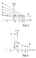
- FIG. 5 shows a graph of the extinction ratio of a peak detector according to the present invention versus temperature, when operated with a fixed resistor in place of a thermistor;
- FIG. 6 shows a graph of the extinction ratio of a peak detector according to the present invention versus temperature
- FIG. 7 shows a graph of the extinction ratio of a peak detector versus temperature employing a range of resistor values
- FIG. 8 shows a graph of the resistor values versus temperature, derived from FIG. 7 .
- FIG. 1 shows, in block diagram form, a peak detector 10 according to the present invention.
- the peak detector 10 receives an input signal v(t) and generates an output signal v o (t).
- the peak detector 10 comprises an input port 12 , an exponential operator 14 , an averaging circuit 16 , a temperature compensator 18 and an output port 20 .
- the input signal v(t) is applied at the input port 12 .
- the input signal v(t) comprises an alternating signal.
- the input signal v(t) is an approximately periodic small amplitude signal. Given its approximately periodic nature, the average value of the amplitude of v(t) is constant with respect to time.
- the input port 12 is connected to the exponential operator 14 .
- the exponential operator 14 modulates the input signal v(t) with an exponential function, such that the upper portion of the periodic signal is amplified to an exponentially greater degree than the lower portion of the signal. Moreover, within the upper portion of the input signal v(t), the higher amplitude portion will be amplified to an exponentially greater degree than the lower amplitude portion of the signal. In a graphical sense, the top portion of the input signal v(t) is ‘stretched’ upwards by the exponential operator. The exponential operator 14 produces an exponentially modulated signal 15 .
- the averaging circuit 16 determines the average amplitude of the exponentially modulated signal 15 . Because the input signal v(t) has been exponentially modulated by the exponential operator 14 , the average value of the exponentially modulated signal 15 is no longer constant. In the periodic input signal v(t) an upper and lower maximum amplitude corresponding to a peak in the signal have the same magnitude and offset each other in the determination of the average value of the input signal v(t). In the exponentially modulated signal 15 an upper maximum amplitude is exponentially larger in magnitude than a lower maximum amplitude, thereby causing a higher average value of the exponentially modulated signal 15 . Accordingly, the average value of the exponentially modulated signal 15 will track peaks in the input signal v(t).
- the averaging circuit 16 is coupled to a temperature compensator 18 .
- the operating temperature of the peak detector 10 and its environment may experience wide variations. The change in operating temperature can result in problems with drift in the components or elements comprising the exponential operator 14 or the averaging circuit 16 . Accordingly, the temperature compensator 18 causes the averaging circuit 16 to eliminate temperature-dependent characteristics from the average signal, leaving an output signal v o (t). The output signal v o (t) appears at the output port 20 .
- FIG. 2 shows in block diagram form a peak detector 10 according to the present invention.
- the peak detector 10 comprises the input port 12 , the output port 20 , the exponential operator 14 , the averaging circuit 16 and the temperature compensator 18 .
- the exponential operator 14 comprises a semiconductor junction circuit 22 and a biasing network 24 .
- the exponential modulation of the input signal v(t) is implemented by the semiconductor junction circuit 22 , which includes an semiconductor element with a current-voltage characteristic that includes an exponential region.
- the biasing network 24 sources a biasing current through the semiconductor junction circuit 22 so as to ensure the semiconductor element is forward biased and operating within the exponential region of its current-voltage characteristic. Without the biasing network 24 , the input signal v(t) would need to provide sufficient voltage to forward bias the semiconductor element and cause it to conduct. Because a small amplitude input signal v(t) would not have sufficient voltage to overcome the threshold voltage for operating the semiconductor element and signal information would be lost. Accordingly, the biasing network 24 is necessary for the operation of the peak detector 10 with small amplitude signals.
- FIG. 3 shows a graph 25 of the current-voltage characteristic of a semiconductor junction, and more particularly, a diode.
- the graph 25 displays the forward-bias region of operation.
- the curve 26 depicts the exponential relationship between the current through the diode I D and the voltage across the diode terminals V D .
- the graph 25 also depicts the diode current i(t) produced by a sinusoidal input signal v(t).
- the sinusoidal input signal v(t) has a peak voltage V pk and an average voltage V avg .
- the average voltage V avg is a constant value that does not vary with changes in V pk .
- the diode current i(t) is an exponential function of the input signal v(t), the relationship being defined by the exponential curve 26 .
- the average current I avg is offset from the current corresponding to the average voltage V avg of the input signal v(t) by an offset current I off .
- the offset current I off is a function of the peak value V pk of the input signal v(t), meaning that the average current I avg will vary with changes in V pk . Accordingly, the peak value of a signal can be detected using the average value of an exponential modulation of the signal.
- I D is the current through the diode
- V D is the voltage across the diode
- I s is the reverse saturation current
- V t is the threshold voltage of the semiconductor junction.
- An input signal v(t) may be represented by a sinusoidal source with a frequency of ⁇ and an amplitude of V pk ,
- I _ D 1 2 ⁇ I s ⁇ e V D + V p ⁇ ⁇ k V t + 1 2 ⁇ I s ⁇ e V D - V p ⁇ ⁇ k V t - I s ( 4 )
- the non-linearity of the transfer curve means that the exponential of the first term of Equation (4) is much greater than the exponential of the second term, such that the second term may be ignored.
- FIG. 4 depicts an electrical schematic of an implementation of the peak detector 10 of FIG. 2 .
- the peak detector 10 includes the input port 12 , the output port 20 , the semiconductor junction circuit 22 , the biasing network 24 and the temperature compensator 18 .
- the averaging circuit 16 (FIG. 2) is implemented by an integrator 30 and further includes an inverter with offset 32 .
- the peak detector 10 also includes a coupling capacitor C 1 between the input port 12 and the semiconductor junction 22 to remove DC components of the input signal v(t).
- the semiconductor junction circuit 22 comprises four diodes D 1 , D 2 , D 3 and D 4 and a capacitor C 2 .
- the first diode D 1 and second diode D 2 are connected in parallel, with their anodes coupled to the input port 12 through coupling capacitor C 1 .
- the cathodes of the first and second diodes D 1 , D 2 are coupled to ground through capacitor C 2 .
- the anodes of the third and fourth diodes D 3 , D 4 are connected to the cathodes of the first and second diodes D 1 , D 2 .
- the cathode of the third diode D 3 is connected to ground and the cathode of the fourth diode D 4 is connected to the output port 20 .
- the biasing network 30 comprises two biasing resistors R 1 a, R 1 b and a capacitor C 4 .
- the two biasing resistors R 1 a, R 1 b are connected in series, with the first biasing resistor R 1 a connected to the anodes of the first and second diodes D 1 , D 2 and with the second biasing resistor R 1 b connected to the positive DC voltage supply V cc .
- the capacitor C 4 is connected between ground and the node between the two biasing resistors R 1 a, R 1 b, so as to shunt any AC signals to ground.
- the integrator 30 comprises an operational amplifier A 1 configured as an integrator using a resistor RX and a capacitor C 3 .
- the resistor R 6 couples the inverting input of the operational amplifier A 1 to the anodes of the first and second diodes D 1 , D 2 of the semiconductor junction circuit 22 .
- the capacitor C 3 is configured in a feedback loop, coupling the output of the operational amplifier A 1 to the inverting input of the operational amplifier A 1 .
- a diode D 5 couples the output of the operational amplifier A 1 to the output port 20 .
- the peak detector 10 further includes the inverting offset stage 32 .
- the inverting offset stage 32 includes an operational amplifier A 2 and three resistors R 3 , R 4 , R 5 .
- Resistor R 3 is connected between the output port 34 and the inverting input of the operational amplifier A 2 .
- Resistor R 5 couples the inverting input of the operational amplifier A 2 to ground.
- Resistor R 4 is connected in a feedback loop between the output of the operational amplifier A 2 and the inverting input of the operational amplifier A 2 .
- the output of the operational amplifier A 2 is connected to the non-inverting input of the operational amplifier A 1 of the integrator 30 .
- the non-inverting input of the operational amplifier A 2 is connected to the cathodes of the first and second diodes D 1 , D 2 .
- the temperature compensator 18 comprises a thermistor R 7 connected between the output port 20 and ground.
- an input signal v(t) is applied at the input port 12 .
- the coupling capacitor C 1 removes any DC component from the input signal v(t), and passes through an approximately periodic small-amplitude AC signal.
- the biasing network 24 supplies a DC current through the biasing resistors R 1 b, R 1 a to the anode of the first and second diodes D 1 , D 2 .
- AC signals developed in the first biasing resistor R 1 a are shunted to ground through the capacitor C 4 .
- the capacitor C 4 does not pass DC signals, so the total DC current passes through the two biasing resistors R 1 a, R 1 b. Note that all the DC current must flow through the semiconductor junction circuit 22 , because the DC current cannot pass through the coupling capacitor C 1 , the feedback capacitor C 3 and the high impedance of the inverting input to the operational amplifier A 1 .
- the diodes D 1 , D 2 may be provided in a common device package to ensure their properties are as identical as possible. This DC current ensures the semiconductor junctions of the first and second diodes D 1 , D 2 are forward-biased and operating in the exponential region of their current-voltage characteristics.
- the AC input signal v(t) sourced through the coupling capacitor C 1 modulates the DC biasing voltage established by the biasing network, such that the current through the first and second diodes D 1 , D 2 has an AC and a DC component. Due to the capacitor C 2 and the input impedance of the operational amplifier A 2 , the DC current in the first and second diodes D 1 , D 2 must pass through the third and fourth diodes D 3 , D 4 . The AC signal at the centre of the four-diode network is shunted to ground through the capacitor C 2 .
- I D3 and I D4 are purely DC signals due to the capacitor C 2 , which shunts any AC signals to ground.
- Equation (7) can be written as:
- V D3 ⁇ overscore (V) ⁇ D1 +V pk
- V D4 ⁇ overscore (V) ⁇ D1 ⁇ V pk (10)
- the AC voltage appearing at the anodes of the first and second diodes D 1 , D 2 corresponds to the exponentially modulated input signal 15 .
- the exponentially modulated input signal 15 is coupled to the integrator 30 through the resistor R 6 .
- the integrator 30 also has an offset as a result of the connection of the non-inverting input of the operational amplifier A 1 with the output of the inverting offset stage 32 .
- the AC characteristic of the integrator 30 is that of a low pass filter so it is the average value of the voltage at the anodes of the first and second diodes D 1 , D 2 that serves as an input into the integrator 30 .
- v o1 ⁇ ( t ) v o2 ⁇ ( t ) + A int ⁇ ⁇ 0 t ⁇ [ v o2 ⁇ ( ⁇ ) - v i ⁇ ⁇ n ⁇ ( t ) ] ⁇ ⁇ ⁇ ( 11 )
- v o1 (t) is the output of the operational amplifier A 1
- v in (t) is the input voltage from the anodes of the first and second diodes D 1 , D 2
- v o2 (t) is the a, offset voltage at the non-inverting input of the operational amplifier A 1
- the diode D 5 limits the output of the integrator 30 to positive values. The voltage drop across the diode D 5 may be ignored in analysis of the operation of the integrator 30 as any introduced offset voltage will decay to zero in steady-state.
- the gain factor A int determines the rate at which the integrator 30 will reach steady state.
- the integrator 30 reaches steady state when the average input voltage V in equals the offset voltage v o2 .
- the DC signal at the centre of the four-diode network of the semiconductor junction circuit 22 serves as the non-inverted input to the inverter with offset 32 .
- the function of the inverter with offset 32 is to compensate for the DC signal introduced by the biasing network 24 and to adjust the proportionality of the output signal v o (t) to a desired relationship with the peak value of the input signal V pk .
- the output v o2 (offset voltage) of the operational amplifier A 2 reaches steady state when it equals the average input voltage V in .
- the average input voltage can be expressed in terms of the diode voltage V D3 of the third diode D 3 by the relationship:
- V in V D3 + ⁇ overscore (V) ⁇ D1 (14)
- the diode voltage V D3 of the third diode D 3 is the sum of the average input voltage V in and the peak voltage of the input signal V pk .
- the output voltage v o (t) is therefore established as a DC signal corresponding to twice the peak value V pk of the input signal v(t).
- the output voltage v o (t) may be taken across an output resistor connected between the output port 20 and ground.
- the selection of the thermistor R 7 as the appropriate temperature compensator is based upon the operation of the peak detector 10 with a fixed resistor in place of the thermistor R 7 . With a fixed resistor in place, the peak detector 10 is operated with a range of input signals v(t) and over a range of operating temperatures. Mapping the output signal v o (t) under these various operating conditions results in a set of curves that depict the temperature-dependent characteristics of the peak detector 10 . A thermistor is then selected such that its characteristic variation matches, as closely as possible, the temperature-dependent variations in the peak detector 10 . Temperature-dependent changes in the output signal v o (t) are thereby cancelled or reduced, improving the extinction ratio of the peak detector 10 and, thus, its bit error rate.
- FIG. 5 shows a graph 60 of the extinction ratio for the peak detector 10 for three values of a fixed resistor in place of thermistor R 7 over a range of operating ambient temperatures. Measurements are made and extinction ratios are calculated at ⁇ 5° C., 10° C., 25° C., 40° C., 55° C. and 70° C.
- the component values of the three resistors R 7 are 30 Ohms, 50 Ohms and 500 Ohms.
- the 30 Ohm resistor results in the higher extinction ratio curve 50 ; the 50 Ohm resistor results in the middle extinction ratio curve 52 ; and the 500 Ohms resistor results in the lower extinction ratio curve 54 .
- a thermistor with a negative coefficient has a resistance that decreases in response to increasing temperature in a non-linear relationship. Accordingly, the thermistor R 7 may compensate for temperature-dependent variations in the extinction ratio.
- thermistor R 7 To determine an appropriate thermistor R 7 , a family of curves representing the extinction ration versus temperature relationship for a range of fixed resistor values is plotted. Reference is made to FIG. 7, which shows a graph of extinction ratio versus temperature for resistors R A , R B , R C , R D and R E . The graph results in five curves. By selecting a desired constant extinction ratio line 64 , one obtains intersection points A, B, C, D and E indicating the resistor value necessary at respective temperatures T A , T B , T C , T D and T E to achieve the desired extinction ratio.
- FIG. 8 shows a graph of the intersection points A, B, C, D and E as a function of resistance and temperature.
- the graph results in a curve 66 of a relationship between resistance and temperature. This relationship is the desired characteristic of the thermistor R 7 . Accordingly, a thermistor R 7 is selected to match, as closely as possible, the curve 66 .
- FIG. 6 shows a graph 62 of the extinction ratio for the peak detector 10 over a range of temperatures.
- the graph 62 includes a sloped curve 56 depicting the relationship between temperature and extinction ratio when a fixed resistor is used in place of thermistor R 7 .
- the sloped curve 56 demonstrates that the extinction ratio deteriorates at higher operating temperatures to unacceptably low levels.
- the graph 62 further includes a substantially flat curve 58 depicting the relationship between temperature and extinction ratio when the peak detector 10 is operated with the thermistor R 7 in place.
- the substantially flat curve 58 demonstrates that the non-linear characteristics of the thermistor R 7 compensate for non-linear temperature variations in the peak detector 10 to result in a substantially constant extinction ratio at an acceptably high level.
Landscapes
- Physics & Mathematics (AREA)
- General Physics & Mathematics (AREA)
- Measurement Of Current Or Voltage (AREA)
Abstract
Description


Claims (23)
Priority Applications (1)
| Application Number | Priority Date | Filing Date | Title |
|---|---|---|---|
| US09/975,965 US6489812B1 (en) | 2001-07-31 | 2001-10-15 | Temperature-compensated small signal peak detector |
Applications Claiming Priority (2)
| Application Number | Priority Date | Filing Date | Title |
|---|---|---|---|
| US30857401P | 2001-07-31 | 2001-07-31 | |
| US09/975,965 US6489812B1 (en) | 2001-07-31 | 2001-10-15 | Temperature-compensated small signal peak detector |
Publications (1)
| Publication Number | Publication Date |
|---|---|
| US6489812B1 true US6489812B1 (en) | 2002-12-03 |
Family
ID=26976312
Family Applications (1)
| Application Number | Title | Priority Date | Filing Date |
|---|---|---|---|
| US09/975,965 Expired - Lifetime US6489812B1 (en) | 2001-07-31 | 2001-10-15 | Temperature-compensated small signal peak detector |
Country Status (1)
| Country | Link |
|---|---|
| US (1) | US6489812B1 (en) |
Cited By (5)
| Publication number | Priority date | Publication date | Assignee | Title |
|---|---|---|---|---|
| US20040085129A1 (en) * | 2002-10-30 | 2004-05-06 | Shuyun Zhang | Power controller circuit for a power amplifier stage |
| US6762627B1 (en) | 2003-03-31 | 2004-07-13 | Micrel, Incorporated | Switched capacitor peak detector with variable time constant asymmetrical filtering |
| US20070257873A1 (en) * | 2004-10-04 | 2007-11-08 | Koninklijke Philips Electronics, N.V. | Brightness control of a lighting unit of a matrix display device |
| US9077445B2 (en) | 2013-07-10 | 2015-07-07 | Qualcomm Incorporated | Temperature compensated RF peak detector |
| CN109324225A (en) * | 2018-11-15 | 2019-02-12 | 国网山东省电力公司电力科学研究院 | A High Precision Current Sampling System for CVT Online Monitoring |
Citations (4)
| Publication number | Priority date | Publication date | Assignee | Title |
|---|---|---|---|---|
| US3700920A (en) * | 1971-05-06 | 1972-10-24 | Bendix Corp | Frequency independent peak detector |
| US5585748A (en) * | 1994-07-01 | 1996-12-17 | Nippondenso Co., Ltd. | Voltage-frequency converter circuit with temperature compensation |
| US6064238A (en) | 1998-10-21 | 2000-05-16 | Nortel Networks Corporation | Low amplitude peak detector |
| US6233440B1 (en) * | 1998-08-05 | 2001-05-15 | Triquint Semiconductor, Inc. | RF power amplifier with variable bias current |
-
2001
- 2001-10-15 US US09/975,965 patent/US6489812B1/en not_active Expired - Lifetime
Patent Citations (4)
| Publication number | Priority date | Publication date | Assignee | Title |
|---|---|---|---|---|
| US3700920A (en) * | 1971-05-06 | 1972-10-24 | Bendix Corp | Frequency independent peak detector |
| US5585748A (en) * | 1994-07-01 | 1996-12-17 | Nippondenso Co., Ltd. | Voltage-frequency converter circuit with temperature compensation |
| US6233440B1 (en) * | 1998-08-05 | 2001-05-15 | Triquint Semiconductor, Inc. | RF power amplifier with variable bias current |
| US6064238A (en) | 1998-10-21 | 2000-05-16 | Nortel Networks Corporation | Low amplitude peak detector |
Cited By (8)
| Publication number | Priority date | Publication date | Assignee | Title |
|---|---|---|---|---|
| US20040085129A1 (en) * | 2002-10-30 | 2004-05-06 | Shuyun Zhang | Power controller circuit for a power amplifier stage |
| WO2004042918A1 (en) * | 2002-10-30 | 2004-05-21 | Analog Devices, Inc. | Power controller circuit for a power amplifier stage |
| US6747516B2 (en) * | 2002-10-30 | 2004-06-08 | Analog Devices, Inc. | Power controller circuit for a power amplifier stage |
| US6762627B1 (en) | 2003-03-31 | 2004-07-13 | Micrel, Incorporated | Switched capacitor peak detector with variable time constant asymmetrical filtering |
| US20070257873A1 (en) * | 2004-10-04 | 2007-11-08 | Koninklijke Philips Electronics, N.V. | Brightness control of a lighting unit of a matrix display device |
| US9077445B2 (en) | 2013-07-10 | 2015-07-07 | Qualcomm Incorporated | Temperature compensated RF peak detector |
| CN109324225A (en) * | 2018-11-15 | 2019-02-12 | 国网山东省电力公司电力科学研究院 | A High Precision Current Sampling System for CVT Online Monitoring |
| CN109324225B (en) * | 2018-11-15 | 2021-05-28 | 国网山东省电力公司电力科学研究院 | A High Precision Current Sampling System for CVT Online Monitoring |
Similar Documents
| Publication | Publication Date | Title |
|---|---|---|
| US6373236B1 (en) | Temperature compensated power detector | |
| CA1085462A (en) | Automatic bias control circuit for injection lasers | |
| KR101056003B1 (en) | Extended Range RMS-DC Converters | |
| JPH0440105A (en) | Linear amplifier circuit | |
| US6291984B1 (en) | Dual mode diode power sensor with square law and linear operating regions | |
| EP3729108B1 (en) | Power detector for radiofrequency power amplifier circuits | |
| US4970456A (en) | Temperature compensated power detector | |
| US6407603B2 (en) | Analog voltage isolation circuit | |
| US6489812B1 (en) | Temperature-compensated small signal peak detector | |
| CN1154183A (en) | Offset-compensated linear RF detector | |
| US4709154A (en) | Opto-electrical signal converter with stabilization | |
| US5732332A (en) | Transmitter having temperature-compensated detector | |
| US6429638B1 (en) | N-diode peak detector | |
| US7622981B2 (en) | Square cell having wide dynamic range and power detector implementing same | |
| JP3404209B2 (en) | Transimpedance amplifier circuit | |
| US3100876A (en) | Transistor amplifier having low output noise | |
| US6968249B2 (en) | Current measuring circuit for measuring drive current to load | |
| JPH10221385A (en) | Temperature compensation circuit | |
| US20040263250A1 (en) | Circuit arrangement having a transimpedance amplifier connected to a current limiter circuit | |
| EP0618452B1 (en) | An average power detector circuit | |
| Aparici | A wide dynamic range square-law diode detector (for radioastronomy) | |
| JP2680807B2 (en) | Amplifier circuit for diode detection output | |
| JP5003245B2 (en) | Voltage generator | |
| JPH10284961A (en) | Voltage control type controller | |
| JPS5947356B2 (en) | Logarithmic conversion circuit for resistance change sensor |
Legal Events
| Date | Code | Title | Description |
|---|---|---|---|
| AS | Assignment |
Owner name: NORTEL NETWORKS LIMITED, CANADA Free format text: ASSIGNMENT OF ASSIGNORS INTEREST;ASSIGNORS:SAVARD, CHRISTIAN S.;DOUNETAS, JACK;BANIC, DEJAN;REEL/FRAME:013160/0902 Effective date: 20010711 |
|
| STCF | Information on status: patent grant |
Free format text: PATENTED CASE |
|
| FPAY | Fee payment |
Year of fee payment: 4 |
|
| AS | Assignment |
Owner name: CIENA LUXEMBOURG S.A.R.L.,LUXEMBOURG Free format text: ASSIGNMENT OF ASSIGNORS INTEREST;ASSIGNOR:NORTEL NETWORKS LIMITED;REEL/FRAME:024213/0653 Effective date: 20100319 Owner name: CIENA LUXEMBOURG S.A.R.L., LUXEMBOURG Free format text: ASSIGNMENT OF ASSIGNORS INTEREST;ASSIGNOR:NORTEL NETWORKS LIMITED;REEL/FRAME:024213/0653 Effective date: 20100319 |
|
| AS | Assignment |
Owner name: CIENA CORPORATION,MARYLAND Free format text: ASSIGNMENT OF ASSIGNORS INTEREST;ASSIGNOR:CIENA LUXEMBOURG S.A.R.L.;REEL/FRAME:024252/0060 Effective date: 20100319 Owner name: CIENA CORPORATION, MARYLAND Free format text: ASSIGNMENT OF ASSIGNORS INTEREST;ASSIGNOR:CIENA LUXEMBOURG S.A.R.L.;REEL/FRAME:024252/0060 Effective date: 20100319 |
|
| FPAY | Fee payment |
Year of fee payment: 8 |
|
| FPAY | Fee payment |
Year of fee payment: 12 |
|
| AS | Assignment |
Owner name: DEUTSCHE BANK AG NEW YORK BRANCH, NEW YORK Free format text: SECURITY INTEREST;ASSIGNOR:CIENA CORPORATION;REEL/FRAME:033329/0417 Effective date: 20140715 |
|
| AS | Assignment |
Owner name: BANK OF AMERICA, N.A., AS ADMINISTRATIVE AGENT, NORTH CAROLINA Free format text: PATENT SECURITY AGREEMENT;ASSIGNOR:CIENA CORPORATION;REEL/FRAME:033347/0260 Effective date: 20140715 Owner name: BANK OF AMERICA, N.A., AS ADMINISTRATIVE AGENT, NO Free format text: PATENT SECURITY AGREEMENT;ASSIGNOR:CIENA CORPORATION;REEL/FRAME:033347/0260 Effective date: 20140715 |
|
| AS | Assignment |
Owner name: CIENA CORPORATION, MARYLAND Free format text: RELEASE BY SECURED PARTY;ASSIGNOR:DEUTSCHE BANK AG NEW YORK BRANCH;REEL/FRAME:050938/0389 Effective date: 20191028 |
|
| AS | Assignment |
Owner name: BANK OF AMERICA, N.A., AS COLLATERAL AGENT, ILLINO Free format text: PATENT SECURITY AGREEMENT;ASSIGNOR:CIENA CORPORATION;REEL/FRAME:050969/0001 Effective date: 20191028 Owner name: BANK OF AMERICA, N.A., AS COLLATERAL AGENT, ILLINOIS Free format text: PATENT SECURITY AGREEMENT;ASSIGNOR:CIENA CORPORATION;REEL/FRAME:050969/0001 Effective date: 20191028 |
|
| AS | Assignment |
Owner name: CIENA CORPORATION, MARYLAND Free format text: RELEASE BY SECURED PARTY;ASSIGNOR:BANK OF AMERICA, N.A.;REEL/FRAME:065630/0232 Effective date: 20231024 |