US6480053B1 - Semiconductor device having an internal power supply circuit - Google Patents
Semiconductor device having an internal power supply circuit Download PDFInfo
- Publication number
- US6480053B1 US6480053B1 US09/587,474 US58747400A US6480053B1 US 6480053 B1 US6480053 B1 US 6480053B1 US 58747400 A US58747400 A US 58747400A US 6480053 B1 US6480053 B1 US 6480053B1
- Authority
- US
- United States
- Prior art keywords
- voltage
- circuit
- power supply
- internal power
- test mode
- Prior art date
- Legal status (The legal status is an assumption and is not a legal conclusion. Google has not performed a legal analysis and makes no representation as to the accuracy of the status listed.)
- Expired - Lifetime
Links
Images


Classifications
-
- G—PHYSICS
- G11—INFORMATION STORAGE
- G11C—STATIC STORES
- G11C11/00—Digital stores characterised by the use of particular electric or magnetic storage elements; Storage elements therefor
- G11C11/21—Digital stores characterised by the use of particular electric or magnetic storage elements; Storage elements therefor using electric elements
- G11C11/34—Digital stores characterised by the use of particular electric or magnetic storage elements; Storage elements therefor using electric elements using semiconductor devices
- G11C11/40—Digital stores characterised by the use of particular electric or magnetic storage elements; Storage elements therefor using electric elements using semiconductor devices using transistors
- G11C11/401—Digital stores characterised by the use of particular electric or magnetic storage elements; Storage elements therefor using electric elements using semiconductor devices using transistors forming cells needing refreshing or charge regeneration, i.e. dynamic cells
- G11C11/4063—Auxiliary circuits, e.g. for addressing, decoding, driving, writing, sensing or timing
- G11C11/407—Auxiliary circuits, e.g. for addressing, decoding, driving, writing, sensing or timing for memory cells of the field-effect type
- G11C11/4074—Power supply or voltage generation circuits, e.g. bias voltage generators, substrate voltage generators, back-up power, power control circuits
-
- G—PHYSICS
- G11—INFORMATION STORAGE
- G11C—STATIC STORES
- G11C29/00—Checking stores for correct operation ; Subsequent repair; Testing stores during standby or offline operation
- G11C29/04—Detection or location of defective memory elements, e.g. cell constructio details, timing of test signals
- G11C29/08—Functional testing, e.g. testing during refresh, power-on self testing [POST] or distributed testing
- G11C29/12—Built-in arrangements for testing, e.g. built-in self testing [BIST] or interconnection details
- G11C29/12005—Built-in arrangements for testing, e.g. built-in self testing [BIST] or interconnection details comprising voltage or current generators
-
- G—PHYSICS
- G05—CONTROLLING; REGULATING
- G05F—SYSTEMS FOR REGULATING ELECTRIC OR MAGNETIC VARIABLES
- G05F1/00—Automatic systems in which deviations of an electric quantity from one or more predetermined values are detected at the output of the system and fed back to a device within the system to restore the detected quantity to its predetermined value or values, i.e. retroactive systems
- G05F1/10—Regulating voltage or current
- G05F1/46—Regulating voltage or current wherein the variable actually regulated by the final control device is DC
- G05F1/462—Regulating voltage or current wherein the variable actually regulated by the final control device is DC as a function of the requirements of the load, e.g. delay, temperature, specific voltage/current characteristic
- G05F1/465—Internal voltage generators for integrated circuits, e.g. step down generators
-
- H—ELECTRICITY
- H03—ELECTRONIC CIRCUITRY
- H03K—PULSE TECHNIQUE
- H03K17/00—Electronic switching or gating, i.e. not by contact-making and –breaking
- H03K17/51—Electronic switching or gating, i.e. not by contact-making and –breaking characterised by the components used
- H03K17/56—Electronic switching or gating, i.e. not by contact-making and –breaking characterised by the components used by the use, as active elements, of semiconductor devices
- H03K17/687—Electronic switching or gating, i.e. not by contact-making and –breaking characterised by the components used by the use, as active elements, of semiconductor devices the devices being field-effect transistors
- H03K17/693—Switching arrangements with several input- or output-terminals, e.g. multiplexers, distributors
Definitions
- This invention relates to a semiconductor device having an internal power supply circuit, which can change an internal-power-supply-voltage.
- a substrate voltage detecting circuit is used especially to supply a stationary and stable substrate voltage to a cell array portion of a dynamic memory having a triple well.
- a voltage conversion circuit comprising a reference voltage generating means for generating a plurality of reference voltages at different levels out of an externally supplied power supply voltage, a selection means for selecting one of said plurality of reference voltages in response to an externally given control signal and an outputting means for supplying the selected reference voltage to said internal circuit.
- the object of the present invention is to provide a semiconductor device having an internal power supply circuit that can change an internal-power-supply-voltage so that an accelerated test can be implemented effectively.
- a semiconductor device having an internal power supply circuit comprises: a substrate voltage detecting circuit which detects a substrate voltage of the semiconductor device having an internal power supply circuit and outputs the first level signal when the substrate voltage exceeds a reference voltage; a control circuit which lowers said substrate voltage when the output signal of the substrate voltage detecting circuit is switched to said first level; and a voltage setting circuit which inputs the first signal indicating a test mode and sets said reference voltage of said substrate voltage detecting circuit either lower or higher than that of normal operation.
- This semiconductor device has a substrate voltage control circuit that inputs the second signal indicating a test mode and increases said substrate voltage
- the substrate voltage control circuit comprises a flip flop circuit that inputs said second signal, an output signal of said substrate voltage detecting circuit and a signal initializing a contact voltage when the voltage is supplied, a voltage conversion circuit that converts the voltage of the output signal given by the flip flop circuit, a resistance connected between said substrate and the ground, and transistors that are connected in series to said resistance and input the output of said voltage conversion circuit to the gates thereof, and is constituted so that in receiving said second signal, said flip flop circuit may be set, and in receiving the output signal of said substrate voltage detecting circuit, said flip flop circuit may be reset, enabling the substrate voltage to increase.
- a semiconductor device having an internal power supply circuit comprises: a reference voltage generation circuit which generates a plurality of output signals of reference voltage; a selection circuit which makes a selection of said output signals in accordance with the first signals indicating a test mode; a voltage comparison circuit which compares the output signals of said selection circuit and the internal-power-supply-voltage; and an internal power supply control circuit which controls said internal-power-supply-voltage to the reference voltage in accordance with the comparison results given by the voltage comparison circuit.
- the semiconductor device having this internal power supply circuit has a transistor that is connected between said internal-power-supply-voltage and the ground, and that inputs the second signals indicating a test mode via the gates thereof, and said test mode lowers the internal-power-supply-voltage
- said second signals go high for a fixed period of time and cause said transistors to turn on for a fixed period of time and accordingly, the internal-power-supply-voltage to be able to be effectively lowered.
- the present invention can change the internal-power-supply-voltage through the use of the first or second signals and set a substrate voltage or the internal-power-supply-voltage at a plurality of voltage, acceleration of tests can be effectively be realized.
- FIG. 1 is a circuit diagram showing a substrate voltage detecting circuit of the semiconductor device having an internal power supply circuit, relating to the first embodiment of the present invention.
- FIG. 2 is a circuit diagram showing the substrate voltage control circuit of the above device.
- FIG. 3 is a timing chart showing the operation of said substrate voltage detecting circuit.
- FIG. 4 is a timing chart showing the operation of the circuit when a substrate voltage is set low.
- FIG. 5 is a timing chart showing the operation of the circuit when a substrate voltage is set high.
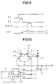
- FIG. 6 is a circuit diagram showing the semiconductor device having an internal power supply circuit, relating to the second embodiment of the present invention.
- FIG. 7 is a timing chart showing the operation of said circuit when an internal power-supply-voltage is set high.
- FIG. 8 is a timing chart showing the operation of said circuit when an internal-power-supply-voltage is set low.
- FIGS. 1 and 2 illustrate a semiconductor device having an internal power supply circuit of the present invention and FIG. 1 shows a substrate voltage detecting circuit 100 and FIG. 2 shows a substrate voltage control circuit 101 , respectively.
- the substrate voltage detecting circuit 100 shown in FIG. 1 comprises a plurality (three in the drawing) of P-channel transistors 1 of Group A, to whose gate a GND level is given, and a plurality (three in the drawing) of P-channel transistors 2 of Group B, to whose gate a substrate voltage VBB is given, and a plurality (two in the drawing) of inverters 3 .
- the inverter 3 at the last stage gives an output signal SUBUP. While the P-channel transistors 1 are connected in series between the voltage supply VCC and the node C, the P-channel transistors 2 are connected in series between the node C and the N-channel transistor 4 .
- the inverters 3 are connected in series between the node C and the output terminal of the output signal SUBUP.
- the N-channel transistor 4 is connected between the ground and the P-channel transistor 2 that is located closest to the ground, and a signal ⁇ 1 (the first signal) is inputted to the gate of the N-channel transistor 4 .
- the N-channel transistor 5 is connected between the node that is located between the P-channel transistor 2 closest to the node C and the P-channel transistor 2 at the next stage, out of the P-channel transistors 2 of Group B, and the ground, and a signal ⁇ 2 (the first signal) is inputted to the gate of the N-channel transistor 5 .
- the N-channel transistor 6 is connected between the node located between the P-channel transistor 2 closest to the ground side and the P-channel transistor 2 at the next stage, out of the P-channel transistors 2 of Group B, and the ground, and an output signal of the NOR circuit 7 which conducts NOR logical operation of the signals ⁇ 1 and ⁇ 2 is inputted to the gate of the N-channel transistor 6 .
- the output terminal (not shown) of the output signal SUBUP is connected to a control circuit that lowers a substrate voltage, and when the SUBUP signal is at an H level, the control circuit that lowers a substrate voltage is powered and lowers a substrate voltage.
- the gate voltage determines the amount of electric current passing through the P-channel transistors 1 and 2 , of Groups A and B, shown in FIG. 1 .
- the changes in the substrate voltage affect the current performance of the P-channel transistors 2 of Group B and accordingly the voltage of the node C changes.
- the signal SUBUP that controls the substrate voltage is generated. More specifically, when the substrate voltage goes up, the current performance of the P-channel transistors 2 of Group B goes down and the voltage at the node C goes up. In contrast with this, when the substrate voltage goes down, the current performance of the P-channel transistors 2 of Group B goes up and the voltage at the node C goes down.
- balance between the P-channel transistors 1 and 2 , of Groups A and B determines the voltage at the node C.
- the voltage at the node C is outputted as the detection signal SUBUP through the inverter 3 at the next stage. More specifically, when the substrate voltage exceeds a desired voltage, the P-channel transistors 1 and 2 , of Groups A and B adjust themselves in size so that the output signal, SUBUP, may change from an L output to an H output.
- the output signals, SUBUP are input to the control circuit that lowers the substrate voltage, and when SUBUP changes to an H level, this control circuit is powered and lowers the substrate voltage to a desired voltage.
- the N-channel transistors from 4 to 7 which characterize the present invention, have a function of changing the substrate voltage where the current performance of the P-channel transistors 1 and 2 , of Groups B and A is balanced, by modifying the effective number of the P-channel transistors 2 of Group B.
- the substrate voltage can be altered when the output signal, SUBUP, changes from an L output to an H output.
- the substrate voltage control circuit 101 is furnished.
- the substrate voltage control circuit 101 is used to increase the substrate voltage by design.
- This substrate voltage control circuit 101 comprises a flip flop circuit 10 that inputs a test mode input signal ⁇ 3 , a substrate voltage detecting signal SUBUP that detects the above-mentioned substrate voltage, and a signal PONA that initializes a contact voltage at the time of voltage supply, a voltage conversion circuit 11 that converts a voltage of the output signal of the flip flop circuit 10 .
- the flip flop circuit 10 includes a 2 input NAND circuit 14 a and 3 input NAND circuit 14 b , and at the input terminals which is one of 2 input NAND circuit 14 a , which is one of the NAND circuits of the flip flop circuit 10 ,the second signal ⁇ 3 indicating a test mode is inputted via an inverter 13 and at the other input terminal thereof the output of the other circuit, 3 input NAND circuit 14 b is inputted.
- 3 input NAND circuit 14 b which is the other circuit of NAND circuits
- the output signal SUBUP of the substrate voltage detecting circuit 100 is inputted via the inverter 13 and at the other two input terminals of 3 input NAND circuit 14 b the output of 2 input NAND circuit 14 a and the signal PONA are inputted.
- the voltage conversion circuit 11 comprises an inverter 15 , P-channel transistors 16 and 17 , and N-channel transistors 18 and 19 .
- the substrate is connected to GND via the resistance 20 and the N-channel transistor 12 and the gate of the N-channel transistor 12 is connected to the flip flop circuit 10 via the voltage conversion circuit 11 .
- the input signal ⁇ 3 is given so that this control circuit may be powered only when entering a test mode that makes a preset value of the substrate voltage exceed a voltage of normal operation.
- the output signal SUBUP is at an L level.
- the current performance of the P-channel transistors 2 of Group B becomes below that of the P-channel transistors 1 of Group A and as a result, the voltage at the node C goes up and exceeds the threshold of the inverter 3 at the next stage, changing the output signal SUBUP to an H level and operating the control circuit that makes the substrate voltage as low as the desired voltage.
- this control circuit makes the substrate voltage as low as the desired voltage V 3 , the voltage at the node C goes down below the threshold of the inverter 3 at the next stage, changing the output signal SUBUP to an L level and susupending the control circuit.
- the signal ⁇ 1 When entering the test mode 1 , the signal ⁇ 1 is changed to an H level, turning on the transistor 4 and turning off the transistors 5 and 6 .
- the electric current passing through the P-channel transistors 1 of Group A goes to the GND via three P-channel transistors 2 of Group B and the N-channel transistor 4 .
- the output signal SUBUP outputs at an H level when the substrate voltage is at V 3 at the time of normal operation, the substrate voltage control circuit is in motion and the substrate voltage becomes lower than that of normal operation.
- the node C When the substrate voltage is reduced to V 2 , the node C has a voltage that becomes below the threshold of the inverter 3 at the next stage, and the output signal SUBUP is changed to an L level, suspending the substrate voltage control circuit. Consequently the substrate voltage becomes stable at V 2 , lower than that of normal operation V 3 .
- the operation when the substrate voltage is set higher than that of normal operation will be explained with reference to the timing chart of FIG. 5 .
- the input signal ⁇ 2 is changed to an H level, turning on the transistor 5 and turning off the transistors 4 and 6 .
- the electric current passing through Group A goes to GND via one P-channel transistor 2 of Group B and the N-channel transistor 5 .
- the current performance of the P-channel transistors 2 of Group B exceeds that of normal operation and so, the node C becomes stable at a voltage lower than that of normal operation. Consequently, a reference voltage, which changes the output signal SUBUP to an H level, becomes V 2 higher than that of normal operation.
- the signal ⁇ 3 is produced from the signal ⁇ 2 .
- This signal ⁇ 3 is a signal that sets the control circuit, shown in FIG. 2, which increases the substrate voltage.
- the signal ⁇ 3 sets the flip flop circuit 10 and turns on the N-channel transistor 12 connecting between GND and the substrate voltage VBB via the resistance 20 .
- the electric current passes from GND to the substrate voltage and the substrate voltage exceeds the substrate voltage V 3 at normal operation.
- the substrate voltage detecting circuit 100 inputs a SUBUP signal.
- the signal resets the RS flip flop circuit 10 and turns off the N-channel transistor 12 , stopping the flow of the electric current into the substrate voltage.
- the substrate voltage may exceed the desired voltage V 1 , but by the signal SUBUP the control circuit that lowers the substrate voltage operates, the substrate voltage being stable at the desired voltage V 1 .
- the substrate voltage can be made either higher or lower than that of normal operation through the use of the test modes, and so by changing the substrate voltage when hold tests in a selection process are conducted, the tests can be accelerated and selection time can be shorted.
- test-mode-based signals are input to the substrate voltage detecting circuit and the substrate voltage is changed by the use of the test modes, but it is also possible to realize the test-mode-based changes of the internal-power-supply-voltage by the use of the reference voltage generating circuit having the other internal power supply circuit.
- the reference voltage generating circuit 21 shown in FIG. 6 generates three different reference voltages, V 4 , V 5 and V 6 (V 4 >V 6 >V 5 ).
- V 4 , V 5 , and V 6 are input to the voltage comparison circuit 22 , which compares the voltage with the internal-power-supply-voltage VINT, via a selection circuit comprised of the N-channel transistors 23 , 24 and 25 , respectively, which respectively receive as inputs the input signals ⁇ 4 and ⁇ 5 and the output signal of the NOR logical circuit 26 via their gates.
- the voltage comparison circuit 22 includes the P-channel transistors 30 and 31 and the N-channel transistors 28 and 29 that are connected between the voltage supply and the ground voltage, and their output signals are input to the gate of the P-channel transistor 32 , connected between the voltage supply and the internal-power-supply-voltage VINT and the ground is connected N-channel transistor 27 .
- a signal ⁇ 6 indicating a second test mode is inputted to the gate of this transistor.
- the input signals ⁇ 4 and ⁇ 5 are at an L level at the time of normal operation and the transistor 25 that receives the output of the NOR logical circuit 26 as an input signal is on and the voltage comparison circuit 22 controls the internal-power-supply-voltage VINT, by comparing the reference voltage V 6 and the internal-power-supply-voltage VINT.
- the input signal ⁇ 4 is changed to an H level, shown in FIG. 7 .
- This turns on the N-channel transistor 23 and turns off the N-channel transistors 24 and 25 .
- the internal-power-supply-voltage is compared with the reference voltage V 4 , which is higher than that of normal operation. As a result, the internal-power-supply-voltage rises to the value V 4 and is kept stable at this level.
- the input signal ⁇ 5 is changed to an H level, shown in FIG. 8 . This turns on the N-channel transistor 24 and off the N-channel transistors 23 and 25 . Thus, the internal-power-supply-voltage is compared with the reference voltage V 5 , which is lower than that of normal operation.
- the signal ⁇ 6 receives the signal ⁇ 5 and is temporarily changed to an H level.
- the input signal ⁇ 6 is input to the gate of the N-channel transistor 27 and when the input signal ⁇ 6 is changed to an H level, it turns on the N-channel transistor 27 .
- This allows internal-power-supply-voltage VINT to fall to the value V 5 . It is, of course, necessary to set the circuit so that the input signal ⁇ 6 may remain at an H level long enough for the internal-power-supply-voltage VINT to be lowered from the voltage V 6 at normal operation, to the desired voltage V 5 .
- test modes can carry out the operation to change the internal-power-supply-voltage.
- the present invention also makes it possible to conduct bump tests that changes voltage during the tests other than the acceleration of the tests by the internal power supply.
- the test modes can be used to make the substrate voltage both higher and lower than that of normal operation, and accordingly when hold tests are conducted during a selection process, changing the substrate voltage can lead to acceleration of the tests and cut-down of the selection time.
Landscapes
- Engineering & Computer Science (AREA)
- Microelectronics & Electronic Packaging (AREA)
- Radar, Positioning & Navigation (AREA)
- Physics & Mathematics (AREA)
- Electromagnetism (AREA)
- General Physics & Mathematics (AREA)
- Automation & Control Theory (AREA)
- Computer Hardware Design (AREA)
- Dram (AREA)
- Tests Of Electronic Circuits (AREA)
- Semiconductor Integrated Circuits (AREA)
- Control Of Voltage And Current In General (AREA)
- For Increasing The Reliability Of Semiconductor Memories (AREA)
Abstract
Description
Claims (4)
Applications Claiming Priority (2)
| Application Number | Priority Date | Filing Date | Title |
|---|---|---|---|
| JP16027899A JP3262103B2 (en) | 1999-06-07 | 1999-06-07 | Semiconductor device having internal power supply circuit |
| JP11-160278 | 1999-06-07 |
Publications (1)
| Publication Number | Publication Date |
|---|---|
| US6480053B1 true US6480053B1 (en) | 2002-11-12 |
Family
ID=15711546
Family Applications (1)
| Application Number | Title | Priority Date | Filing Date |
|---|---|---|---|
| US09/587,474 Expired - Lifetime US6480053B1 (en) | 1999-06-07 | 2000-06-05 | Semiconductor device having an internal power supply circuit |
Country Status (3)
| Country | Link |
|---|---|
| US (1) | US6480053B1 (en) |
| JP (1) | JP3262103B2 (en) |
| KR (1) | KR100387192B1 (en) |
Cited By (3)
| Publication number | Priority date | Publication date | Assignee | Title |
|---|---|---|---|---|
| US20040109368A1 (en) * | 2002-12-03 | 2004-06-10 | Matsushita Electric Industrial Co., Ltd. | Semiconductor integrated circuit device |
| US20100097867A1 (en) * | 2008-10-22 | 2010-04-22 | Samsung Electronics Co., Ltd. | Internal source voltage generating circuit of semiconductor memory device |
| US20120155211A1 (en) * | 2009-09-04 | 2012-06-21 | Panasonic Corporation | Semiconductor integrated circuit |
Families Citing this family (3)
| Publication number | Priority date | Publication date | Assignee | Title |
|---|---|---|---|---|
| KR100452323B1 (en) * | 2002-07-02 | 2004-10-12 | 삼성전자주식회사 | Circuit and method for selecting reference voltage in semiconductor memory device therefor |
| KR100452326B1 (en) * | 2002-07-04 | 2004-10-12 | 삼성전자주식회사 | Method and circuit for selecting mode of operation voltage in semiconductor memory device thereof |
| JP4996215B2 (en) * | 2006-11-28 | 2012-08-08 | ルネサスエレクトロニクス株式会社 | Semiconductor device test method |
Citations (12)
| Publication number | Priority date | Publication date | Assignee | Title |
|---|---|---|---|---|
| US4706013A (en) * | 1986-11-20 | 1987-11-10 | Industrial Technology Research Institute | Matching current source |
| US4763021A (en) * | 1987-07-06 | 1988-08-09 | Unisys Corporation | CMOS input buffer receiver circuit with ultra stable switchpoint |
| US4864216A (en) * | 1989-01-19 | 1989-09-05 | Hewlett-Packard Company | Light emitting diode array current power supply |
| JPH0415949A (en) | 1990-05-09 | 1992-01-21 | Mitsubishi Electric Corp | semiconductor equipment |
| US5317254A (en) * | 1992-09-17 | 1994-05-31 | Micro Control Company | Bipolar power supply |
| JPH07105160A (en) | 1993-10-05 | 1995-04-21 | Mitsubishi Chem Corp | Optical information processing element |
| US5455534A (en) * | 1992-02-14 | 1995-10-03 | Kabushiki Kaisha Toshiba | Semiconductor device for liquid crystal panel driving power supply |
| JPH09145804A (en) | 1995-11-28 | 1997-06-06 | Mitsubishi Electric Corp | Potential detection circuit and semiconductor integrated circuit |
| JPH09153300A (en) | 1995-11-29 | 1997-06-10 | Mitsubishi Electric Corp | Semiconductor device |
| US5689460A (en) * | 1994-08-04 | 1997-11-18 | Mitsubishi Denki Kabushiki Kaisha | Semiconductor memory device with a voltage down converter stably generating an internal down-converted voltage |
| KR19980018101A (en) | 1996-08-02 | 1998-06-05 | 사와무라 시꼬 | Internal power circuit |
| JPH1153894A (en) | 1997-08-04 | 1999-02-26 | Hitachi Ltd | Inspection method and semiconductor integrated circuit device |
Family Cites Families (1)
| Publication number | Priority date | Publication date | Assignee | Title |
|---|---|---|---|---|
| JP7105160B2 (en) | 2018-09-26 | 2022-07-22 | 株式会社やまびこ | stratified scavenging engine and portable work machine |
-
1999
- 1999-06-07 JP JP16027899A patent/JP3262103B2/en not_active Expired - Fee Related
-
2000
- 2000-06-05 KR KR10-2000-0030804A patent/KR100387192B1/en not_active Expired - Fee Related
- 2000-06-05 US US09/587,474 patent/US6480053B1/en not_active Expired - Lifetime
Patent Citations (12)
| Publication number | Priority date | Publication date | Assignee | Title |
|---|---|---|---|---|
| US4706013A (en) * | 1986-11-20 | 1987-11-10 | Industrial Technology Research Institute | Matching current source |
| US4763021A (en) * | 1987-07-06 | 1988-08-09 | Unisys Corporation | CMOS input buffer receiver circuit with ultra stable switchpoint |
| US4864216A (en) * | 1989-01-19 | 1989-09-05 | Hewlett-Packard Company | Light emitting diode array current power supply |
| JPH0415949A (en) | 1990-05-09 | 1992-01-21 | Mitsubishi Electric Corp | semiconductor equipment |
| US5455534A (en) * | 1992-02-14 | 1995-10-03 | Kabushiki Kaisha Toshiba | Semiconductor device for liquid crystal panel driving power supply |
| US5317254A (en) * | 1992-09-17 | 1994-05-31 | Micro Control Company | Bipolar power supply |
| JPH07105160A (en) | 1993-10-05 | 1995-04-21 | Mitsubishi Chem Corp | Optical information processing element |
| US5689460A (en) * | 1994-08-04 | 1997-11-18 | Mitsubishi Denki Kabushiki Kaisha | Semiconductor memory device with a voltage down converter stably generating an internal down-converted voltage |
| JPH09145804A (en) | 1995-11-28 | 1997-06-06 | Mitsubishi Electric Corp | Potential detection circuit and semiconductor integrated circuit |
| JPH09153300A (en) | 1995-11-29 | 1997-06-10 | Mitsubishi Electric Corp | Semiconductor device |
| KR19980018101A (en) | 1996-08-02 | 1998-06-05 | 사와무라 시꼬 | Internal power circuit |
| JPH1153894A (en) | 1997-08-04 | 1999-02-26 | Hitachi Ltd | Inspection method and semiconductor integrated circuit device |
Cited By (7)
| Publication number | Priority date | Publication date | Assignee | Title |
|---|---|---|---|---|
| US20040109368A1 (en) * | 2002-12-03 | 2004-06-10 | Matsushita Electric Industrial Co., Ltd. | Semiconductor integrated circuit device |
| US7102413B2 (en) * | 2002-12-03 | 2006-09-05 | Matsushita Electric Industrial Co., Ltd. | Semiconductor integrated circuit device |
| CN100375194C (en) * | 2002-12-03 | 2008-03-12 | 松下电器产业株式会社 | Semiconductor integrated circuit device |
| US20100097867A1 (en) * | 2008-10-22 | 2010-04-22 | Samsung Electronics Co., Ltd. | Internal source voltage generating circuit of semiconductor memory device |
| US8120971B2 (en) * | 2008-10-22 | 2012-02-21 | Samsung Electronics Co., Ltd. | Internal source voltage generating circuit of semiconductor memory device |
| US20120155211A1 (en) * | 2009-09-04 | 2012-06-21 | Panasonic Corporation | Semiconductor integrated circuit |
| US8520463B2 (en) * | 2009-09-04 | 2013-08-27 | Panasonic Corporation | Semiconductor integrated circuit |
Also Published As
| Publication number | Publication date |
|---|---|
| KR20010049488A (en) | 2001-06-15 |
| JP2000346914A (en) | 2000-12-15 |
| KR100387192B1 (en) | 2003-06-11 |
| JP3262103B2 (en) | 2002-03-04 |
Similar Documents
| Publication | Publication Date | Title |
|---|---|---|
| JP2662345B2 (en) | Internal power supply voltage generation circuit | |
| US7205682B2 (en) | Internal power supply circuit | |
| US6424585B1 (en) | Semiconductor memory device with a voltage down converter stably generating an internal down-converted voltage | |
| JP2994540B2 (en) | Fuse programmable step-down circuit | |
| US6876585B2 (en) | Circuit and method for selecting reference voltages in semiconductor memory device | |
| EP0399240A2 (en) | Semiconductor memory device | |
| US6867641B2 (en) | Internal voltage generator for semiconductor device | |
| US7126872B2 (en) | Semiconductor integrated circuit | |
| EP0205258A2 (en) | Semiconductor integrated circuit having a function for switching the operational modes of an internal circuit | |
| US6456513B2 (en) | Voltage conversion circuit and control circuit therefor | |
| JPH06194424A (en) | Semiconductor apparatus | |
| US6480053B1 (en) | Semiconductor device having an internal power supply circuit | |
| KR100267011B1 (en) | Internal power supply voltage generation circuit of semiconductor memory device | |
| US20210203316A1 (en) | Delay circuits, and related semiconductor devices and methods | |
| US8553487B2 (en) | Internal power supply circuit, semiconductor device, and manufacturing method of semiconductor device | |
| US5786719A (en) | Mode setting circuit and mode setting apparatus used to select a particular semiconductor function | |
| US6614674B2 (en) | Regulator circuit for independent adjustment of pumps in multiple modes of operation | |
| JP2001035199A (en) | Semiconductor device | |
| JPH1092199A (en) | Internal voltage generation circuit | |
| US6738280B2 (en) | Read only memory | |
| JPH0621377A (en) | Semiconductor storage device | |
| KR100817080B1 (en) | A semiconductor memory device capable of independently controlling internal power supply voltages and a method of using the device | |
| US20030151961A1 (en) | Semiconductor memory device having internal circuit screening function | |
| KR100689804B1 (en) | High Voltage Generation Circuit of Semiconductor Memory Device | |
| JPH04311898A (en) | Semiconductor device |
Legal Events
| Date | Code | Title | Description |
|---|---|---|---|
| AS | Assignment |
Owner name: NEC CORPORATION, JAPAN Free format text: ASSIGNMENT OF ASSIGNORS INTEREST;ASSIGNOR:TERAMOTO, KAZUHIRO;REEL/FRAME:010849/0595 Effective date: 20000529 |
|
| STCF | Information on status: patent grant |
Free format text: PATENTED CASE |
|
| AS | Assignment |
Owner name: NEC ELECTRONICS CORPORATION, JAPAN Free format text: ASSIGNMENT OF ASSIGNORS INTEREST;ASSIGNOR:NEC CORPORATION;REEL/FRAME:013717/0650 Effective date: 20030110 |
|
| FPAY | Fee payment |
Year of fee payment: 4 |
|
| AS | Assignment |
Owner name: ELPIDA MEMORY, INC., JAPAN Free format text: ASSIGNMENT OF ASSIGNORS INTEREST;ASSIGNORS:NEC CORPORATION;NEC ELECTRONICS CORPORATION;REEL/FRAME:018545/0737 Effective date: 20060531 |
|
| FPAY | Fee payment |
Year of fee payment: 8 |
|
| AS | Assignment |
Owner name: ELPIDA MEMORY INC., JAPAN Free format text: SECURITY AGREEMENT;ASSIGNOR:PS4 LUXCO S.A.R.L.;REEL/FRAME:032414/0261 Effective date: 20130726 |
|
| FPAY | Fee payment |
Year of fee payment: 12 |
|
| AS | Assignment |
Owner name: PS4 LUXCO S.A.R.L., LUXEMBOURG Free format text: ASSIGNMENT OF ASSIGNORS INTEREST;ASSIGNOR:ELPIDA MEMORY, INC.;REEL/FRAME:032899/0588 Effective date: 20130726 |
|
| AS | Assignment |
Owner name: PS5 LUXCO S.A.R.L., LUXEMBOURG Free format text: ASSIGNMENT OF ASSIGNORS INTEREST;ASSIGNOR:PS4 LUXCO S.A.R.L.;REEL/FRAME:039818/0506 Effective date: 20130829 Owner name: LONGITUDE SEMICONDUCTOR S.A.R.L., LUXEMBOURG Free format text: CHANGE OF NAME;ASSIGNOR:PS5 LUXCO S.A.R.L.;REEL/FRAME:039793/0880 Effective date: 20131112 |
|
| AS | Assignment |
Owner name: LONGITUDE LICENSING LIMITED, IRELAND Free format text: ASSIGNMENT OF ASSIGNORS INTEREST;ASSIGNOR:LONGITUDE SEMICONDUCTOR S.A.R.L.;REEL/FRAME:046867/0248 Effective date: 20180731 |