US6434686B1 - Address generating circuit - Google Patents
Address generating circuit Download PDFInfo
- Publication number
- US6434686B1 US6434686B1 US09/237,804 US23780499A US6434686B1 US 6434686 B1 US6434686 B1 US 6434686B1 US 23780499 A US23780499 A US 23780499A US 6434686 B1 US6434686 B1 US 6434686B1
- Authority
- US
- United States
- Prior art keywords
- data
- address
- read
- counter
- bits
- Prior art date
- Legal status (The legal status is an assumption and is not a legal conclusion. Google has not performed a legal analysis and makes no representation as to the accuracy of the status listed.)
- Expired - Lifetime
Links
Images


Classifications
-
- G—PHYSICS
- G06—COMPUTING OR CALCULATING; COUNTING
- G06F—ELECTRIC DIGITAL DATA PROCESSING
- G06F7/00—Methods or arrangements for processing data by operating upon the order or content of the data handled
- G06F7/76—Arrangements for rearranging, permuting or selecting data according to predetermined rules, independently of the content of the data
- G06F7/78—Arrangements for rearranging, permuting or selecting data according to predetermined rules, independently of the content of the data for changing the order of data flow, e.g. matrix transposition or LIFO buffers; Overflow or underflow handling therefor
- G06F7/785—Arrangements for rearranging, permuting or selecting data according to predetermined rules, independently of the content of the data for changing the order of data flow, e.g. matrix transposition or LIFO buffers; Overflow or underflow handling therefor having a sequence of storage locations each being individually accessible for both enqueue and dequeue operations, e.g. using a RAM
-
- G—PHYSICS
- G06—COMPUTING OR CALCULATING; COUNTING
- G06F—ELECTRIC DIGITAL DATA PROCESSING
- G06F17/00—Digital computing or data processing equipment or methods, specially adapted for specific functions
- G06F17/10—Complex mathematical operations
- G06F17/14—Fourier, Walsh or analogous domain transformations, e.g. Laplace, Hilbert, Karhunen-Loeve, transforms
- G06F17/147—Discrete orthonormal transforms, e.g. discrete cosine transform, discrete sine transform, and variations therefrom, e.g. modified discrete cosine transform, integer transforms approximating the discrete cosine transform
Definitions
- the invention relates to an address generating circuit for generating an access address to a memory for storing data, and more particularly to an address generating circuit suitable to read data, which was written in the memory, with its order changed.
- audio data and image data are encoded and compressed when stored or transmitted, then expanded and decoded when reproduced or received.
- a speech signal is converted into digital data (A/D conversion), which is then divided into three bands such as low, middle, and high (frequency bands) by a digital filter called QMF (Quadrature Mirror Filter).
- the obtained data is subjected to MDCT (Modified Discrete Cosine Transform) processing, quantizing processing, or the like and written on the MD.
- MDCT Modified Discrete Cosine Transform
- IMDCT Inverse MDCT
- IQMF Inverse QMF
- a memory is required in order to store data being processed.
- the memory temporarily stores data being sent from the preceding filter and reads it before the MDCT processing is performed.
- MDCT and IMDCT process data by dividing it into 1SG (sound group) for every 11.6 msec.
- This 1SG corresponds to 1024 words, but MDCT and IMDCT process 1024+192 words in order to overlap slightly data across the boundary of the sound groups. Therefore, IMDCT outputs for example 1024+192 words of data for every 1SG. And, 1024 words of data is supplied to IQMR for every 1SG.
- IMDCT separately outputs data of an L (left) channel and data of a R (right) channel. Specifically, for 1SG of data, data of the L channel is output, then data of the R channel is output. Meanwhile, data of the L channel and that of the R channel are alternately output to IQMF.
- the provision of the capacities for writing and reading for 1SG of data allows to write and read without any problem by switching a writing area and a reading area for every period of 1SG.
- the memory capacity be made as small as possible. Since reading can be made without writing 1SG of data in the memory, the memory capacity may be made small by a device able to manage the memory.
- the invention relates to an address generating circuit for generating an access address to a memory for storing a predetermined amount of data comprising a counter of a predetermined number of bits and which counts prescribed clocks to determine output as an access address, wherein the position of a least significant bit (LSB) of output from the counter is counted in a state shifted by a predetermined number of bits at intervals of predetermined time, and output from the counter is determined as an address.
- LSB least significant bit
- the invention also relates to an address generating circuit for generating a writing address to and a reading address from a memory for storing a predetermined amount of data comprising a write address counter with a predetermined number of bits and which counts a first clock and determines output as a write address; and a read address counter with a predetermined number of bits which counts a second clock and determines output as a read address, wherein the positions of least significant bits (LSB) of output from both counters is shifted by the same number of bits at intervals of predetermined time, the position of a least significant bit of output from the read address counter prior to shifting is corresponded with the shift position of the write address counter after shifting and counted by both the counters. Counting is made by both the counters in this state, and the counted outputs are determined as a write address and a read address.
- LSB least significant bits
- the present invention sequentially writes into areas from which reading is completed. Therefore, total memory capacity can be used efficiently and a need for excessively large capacity can be eliminated.
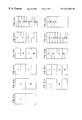
- FIG. 1 is a block diagram showing the configuration of an embodiment of the present invention
- FIG. 2 is a diagram showing writing into a memory
- FIGS. 3 ( a ), 3 ( b ), 3 ( c ), 3 ( d ), 3 ( e ), 3 ( f ), 3 ( g ), 3 ( h ), 3 ( i ), 3 ( j ), 3 ( k ) are diagrams showing a procedure to write into a memory.
- FIG. 1 is a block diagram showing the configuration of the present embodiment, in which data from IMDCT is written as input data into a memory 10 .
- Data read from the memory 10 is sent to IQMF.
- the memory 10 has a capacity of 1024 words and 0-1023 addresses.
- the address for writing input data into the memory 10 is determined by an address signal from a write address counter 12 .
- the write address counter 12 is a 10-bit counter of a 9 , a 8 , a 7 , . . . a 1 , a 0 and counts a write clock WCK to generate 0-1023 addresses.
- the read address to the memory 10 is determined according to an address signal from a read address counter 14 .
- the read address counter 14 is also a 10-bit counter of a 9 , a 8 , a 7 , . . . a 1 , a 0 and counts a read clock RCK to generate 0-1023 addresses.
- the write address counter 12 and the read address counter 14 an change the position of LSB (least significant bit). Specifically, when shift signals SF 1 , SF 2 are entered the write address counter 12 and the read address counter 14 , they are counted with the position of LSB shifted by 3 bits. For example, after a 9 , a 8 , a 7 , a 6 , a 5 , a 4 , a 3 , a 2 , a 1 , a 0 come a 6 , a 5 , a 4 , a 3 , a 2 , a 1 , a 0 , a 9 , a 8 , a 7 . Thus, a 7 becomes LSB, and the write clock WCK or the read clock RCK is counted up.
- the read address counter 14 shifts its inner bits by 3 bits. Specifically, the order is changed to a 6 , a 5 , a 4 , a 3 , a 2 a, a 1 , a 0 , a 9 , a 8 , a 7 , and bit a 7 is determined as LSB to count up.
- the address proceeds by 128, and the words are read one by one in order of the low range, middle range, high range 1 and high range 2 of the L channel and the low range, middle range, high range 1 and high range 2 of the R channel.
- the writing address counter 12 When such writing and reading are performed for a period of 1SG, the writing address counter 12 displaces the bit position by 3 bits. In other words, the write address counter 12 has the same write address as the above-described read address, or as follows.
- the bit position of the read address is shifted by 3 bits after a lapse of 0.5SG. Therefore, it becomes a 3 , a 2 a, a 1 , a 0 , a 9 , a 8 , a 7 , a 6 , a 5 , a 4 . Accordingly, reading is performed successively from the head of the respective areas in which data is written as described above.
- the memory 10 can have a capacity for 1SG only to deal with writing and reading of data.
- two types of data of L and R channels are shown for simplification.
- Data of L and R channels are written in this order, and L and R are successively read for words one by one. Addresses are 0 to 7, and the write address counter 12 and the read address counter 14 are 3 bits of a 2 , a 1 , a 0 .
- the write address counter 12 is used in order of a 2 , a 1 , a 0 to complete writing 0.5SG of data.
- data of the L channel is written at the upper half of the memory 10 as shown in FIG. 3 ( a ).
- reading is started according to the read address counter 14 .
- the read address counter 14 counts in order of a 1 , a 0 , a 2 .
- reading is alternately made from the L and R channels for words one by one as 000, 100, 001, 101, . . .
- memory 10 When writing 1SG of data is complete, memory 10 is as shown in FIG. 3 ( b ). At this point, reading is complete for half of each area of the L and R channels as shown in FIG. 3 ( c ).
- LSB of the write address counter 12 is shifted by 1 bit as a 1 , a 0 , a 2 , which is the same as the above-described read address. Therefore, for a period of 0.5SG after that, data of the L channel is written in the area from which reading has been completed. In other words, data is written in the areas L as shown in FIG. 3 ( d ).
- the position of LSB of the read address counter 14 is shifted.
- the order of bits in the read address counter 14 is a 0 , a 2 , a 1 . Reading from the areas indicated as L and R in FIG. 3 ( g ) is then started.
- writing is complete as shown in FIG. 3 ( j ).
- reading of data from the upper half is complete as shown in FIG. 3 ( k ).
- the order of bits of the write address counter 12 is changed to a 2 , a 1 , a 0 , and writing is started in the order shown in FIG. 3 ( a ).
- the capacity of the memory 10 may correspond with the amount of data input during the period of 1SG.
- reading was switched for every word. Therefore, when the read unit is divided into a single word unit, the next reading is made continuously. By the division of the access address up to this stage, one cycle of the address shift is completed. In other words, the write area and the read area are divided, and when reading becomes continuous, one cycle is completed.
- data can be read or written with a memory of reduced capacity according to the present invention.
Landscapes
- Physics & Mathematics (AREA)
- Engineering & Computer Science (AREA)
- General Physics & Mathematics (AREA)
- Mathematical Physics (AREA)
- Theoretical Computer Science (AREA)
- Mathematical Analysis (AREA)
- Mathematical Optimization (AREA)
- Pure & Applied Mathematics (AREA)
- Computational Mathematics (AREA)
- Data Mining & Analysis (AREA)
- General Engineering & Computer Science (AREA)
- Algebra (AREA)
- Databases & Information Systems (AREA)
- Software Systems (AREA)
- Discrete Mathematics (AREA)
- Memory System (AREA)
- Television Signal Processing For Recording (AREA)
Abstract
Description
Claims (5)
Applications Claiming Priority (2)
| Application Number | Priority Date | Filing Date | Title |
|---|---|---|---|
| JP10-020056 | 1998-01-30 | ||
| JP02005698A JP3639424B2 (en) | 1998-01-30 | 1998-01-30 | Address generation circuit |
Publications (1)
| Publication Number | Publication Date |
|---|---|
| US6434686B1 true US6434686B1 (en) | 2002-08-13 |
Family
ID=12016430
Family Applications (1)
| Application Number | Title | Priority Date | Filing Date |
|---|---|---|---|
| US09/237,804 Expired - Lifetime US6434686B1 (en) | 1998-01-30 | 1999-01-27 | Address generating circuit |
Country Status (2)
| Country | Link |
|---|---|
| US (1) | US6434686B1 (en) |
| JP (1) | JP3639424B2 (en) |
Cited By (4)
| Publication number | Priority date | Publication date | Assignee | Title |
|---|---|---|---|---|
| US20080005519A1 (en) * | 2002-08-28 | 2008-01-03 | Micron Technology, Inc. | Multi-bank memory accesses using posted writes |
| US20100191918A1 (en) * | 2009-01-23 | 2010-07-29 | Korea Advanced Institute Of Science & Technology | Cache Controller Device, Interfacing Method and Programming Method Using the Same |
| US10747725B2 (en) | 2015-07-14 | 2020-08-18 | Fujitsu Limited | Compressing method, compressing apparatus, and computer-readable recording medium |
| CN111915477A (en) * | 2020-08-08 | 2020-11-10 | 湖南润泽医疗影像科技有限公司 | Address rotation method for color ultrasonic Doppler transposition storage |
Citations (4)
| Publication number | Priority date | Publication date | Assignee | Title |
|---|---|---|---|---|
| US5138501A (en) * | 1989-03-17 | 1992-08-11 | Sharp Kabushiki Kaisha | Magnetic recorder/reproducer for recording digital signal on a plurality of tracks of magnetic recording media and reproducing the same |
| US5469269A (en) * | 1991-01-31 | 1995-11-21 | Samsung Electronics Co., Ltd. | High speed optical information system and method |
| US5488658A (en) * | 1993-04-15 | 1996-01-30 | Matsushita Electric Industrial Co., Ltd. | Video signal scrambling and descrambling apparatus |
| US5842169A (en) * | 1995-02-28 | 1998-11-24 | Sanyo Electric Co., Ltd. | Read/write control method and circuit for a sound recording/reproducing device |
-
1998
- 1998-01-30 JP JP02005698A patent/JP3639424B2/en not_active Expired - Fee Related
-
1999
- 1999-01-27 US US09/237,804 patent/US6434686B1/en not_active Expired - Lifetime
Patent Citations (4)
| Publication number | Priority date | Publication date | Assignee | Title |
|---|---|---|---|---|
| US5138501A (en) * | 1989-03-17 | 1992-08-11 | Sharp Kabushiki Kaisha | Magnetic recorder/reproducer for recording digital signal on a plurality of tracks of magnetic recording media and reproducing the same |
| US5469269A (en) * | 1991-01-31 | 1995-11-21 | Samsung Electronics Co., Ltd. | High speed optical information system and method |
| US5488658A (en) * | 1993-04-15 | 1996-01-30 | Matsushita Electric Industrial Co., Ltd. | Video signal scrambling and descrambling apparatus |
| US5842169A (en) * | 1995-02-28 | 1998-11-24 | Sanyo Electric Co., Ltd. | Read/write control method and circuit for a sound recording/reproducing device |
Cited By (8)
| Publication number | Priority date | Publication date | Assignee | Title |
|---|---|---|---|---|
| US20080005519A1 (en) * | 2002-08-28 | 2008-01-03 | Micron Technology, Inc. | Multi-bank memory accesses using posted writes |
| US7916554B2 (en) * | 2002-08-28 | 2011-03-29 | Round Rock Research, Llc | Multi-bank memory accesses using posted writes |
| US20110167237A1 (en) * | 2002-08-28 | 2011-07-07 | Round Rock Research, Llc | Multi-bank memory accesses using posted writes |
| US8154932B2 (en) | 2002-08-28 | 2012-04-10 | Round Rock Research, Llc | Increasing efficiency of memory accesses by selectively introducing a relative delay between the time that write addresses are provided to the memory and the time that write data is provided to the memory |
| US8687436B2 (en) | 2002-08-28 | 2014-04-01 | Round Rock Research, Llc | Increasing efficiency of memory accesses by selectively introducing a relative delay between the time that write addresses are provided to the memory and the time that write data is provided to the memory |
| US20100191918A1 (en) * | 2009-01-23 | 2010-07-29 | Korea Advanced Institute Of Science & Technology | Cache Controller Device, Interfacing Method and Programming Method Using the Same |
| US10747725B2 (en) | 2015-07-14 | 2020-08-18 | Fujitsu Limited | Compressing method, compressing apparatus, and computer-readable recording medium |
| CN111915477A (en) * | 2020-08-08 | 2020-11-10 | 湖南润泽医疗影像科技有限公司 | Address rotation method for color ultrasonic Doppler transposition storage |
Also Published As
| Publication number | Publication date |
|---|---|
| JPH11219316A (en) | 1999-08-10 |
| JP3639424B2 (en) | 2005-04-20 |
Similar Documents
| Publication | Publication Date | Title |
|---|---|---|
| US5913229A (en) | Buffer memory controller storing and extracting data of varying bit lengths | |
| KR100278891B1 (en) | Compressed code decoding device and speech decoding device | |
| JPH02500634A (en) | Digital encoding/decoding method and device | |
| US5570308A (en) | Method of processing digital audio signals of different sampling rates | |
| US6434686B1 (en) | Address generating circuit | |
| GB2434727A (en) | Bit order reversal in Direct Stream Digital data transmission | |
| KR0171851B1 (en) | Multi-Sound Playback Apparatus and Method Using Semiconductor Memory Card | |
| EP0632458B1 (en) | Parallel data outputting storage circuit | |
| US5646906A (en) | Method & Apparatus for real-time processing of moving picture signals using flash memories | |
| EP0679987A2 (en) | Digital data formatting/deformatting circuits | |
| US6260122B1 (en) | Memory device | |
| US20040117542A1 (en) | LIFO type data storage device incorporating two random access memories | |
| USRE36026E (en) | Programmable device for storing digital video lines | |
| KR0115141Y1 (en) | Recording/reproducing apparatus for audio signal | |
| JPH0566673B2 (en) | ||
| JPS59193513A (en) | Interleave circuit | |
| KR100209884B1 (en) | High speed selection reproducing apparatus and method providing multi-output | |
| JPH1098397A (en) | Interleaver | |
| JPH0769720B2 (en) | Voice recording / playback device | |
| JP3682863B2 (en) | Speech decoding method and speech decoding apparatus | |
| JPS61271671A (en) | Processing device for error information | |
| JPS6034126B2 (en) | Digital signal function conversion circuit | |
| JPS59223845A (en) | Shift register circuit using ram | |
| JPH088865A (en) | Voice data processor | |
| JPS6141296A (en) | Exchange switch system |
Legal Events
| Date | Code | Title | Description |
|---|---|---|---|
| AS | Assignment |
Owner name: SANYO ELECTRIC CO., LTD., JAPAN Free format text: ASSIGNMENT OF ASSIGNORS INTEREST;ASSIGNORS:MATSUI, MASARU;FUMA, MASATO;REEL/FRAME:009728/0024 Effective date: 19981216 |
|
| STCF | Information on status: patent grant |
Free format text: PATENTED CASE |
|
| FEPP | Fee payment procedure |
Free format text: PAYOR NUMBER ASSIGNED (ORIGINAL EVENT CODE: ASPN); ENTITY STATUS OF PATENT OWNER: LARGE ENTITY |
|
| FPAY | Fee payment |
Year of fee payment: 4 |
|
| FPAY | Fee payment |
Year of fee payment: 8 |
|
| FEPP | Fee payment procedure |
Free format text: PAYOR NUMBER ASSIGNED (ORIGINAL EVENT CODE: ASPN); ENTITY STATUS OF PATENT OWNER: LARGE ENTITY |
|
| AS | Assignment |
Owner name: SEMICONDUCTOR COMPONENTS INDUSTRIES, LLC, ARIZONA Free format text: ASSIGNMENT OF ASSIGNORS INTEREST;ASSIGNOR:SANYO ELECTRIC CO., LTD.;REEL/FRAME:026594/0385 Effective date: 20110101 |
|
| FPAY | Fee payment |
Year of fee payment: 12 |
|
| AS | Assignment |
Owner name: SEMICONDUCTOR COMPONENTS INDUSTRIES, LLC, ARIZONA Free format text: CORRECTIVE ASSIGNMENT TO CORRECT THE INCORRECT #12/577882 PREVIOUSLY RECORDED ON REEL 026594 FRAME 0385. ASSIGNOR(S) HEREBY CONFIRMS THE ASSIGNMENT;ASSIGNOR:SANYO ELECTRIC CO., LTD;REEL/FRAME:032836/0342 Effective date: 20110101 |
|
| AS | Assignment |
Owner name: DEUTSCHE BANK AG NEW YORK BRANCH, NEW YORK Free format text: SECURITY INTEREST;ASSIGNOR:SEMICONDUCTOR COMPONENTS INDUSTRIES, LLC;REEL/FRAME:038620/0087 Effective date: 20160415 |
|
| AS | Assignment |
Owner name: DEUTSCHE BANK AG NEW YORK BRANCH, AS COLLATERAL AG Free format text: CORRECTIVE ASSIGNMENT TO CORRECT THE INCORRECT PATENT NUMBER 5859768 AND TO RECITE COLLATERAL AGENT ROLE OF RECEIVING PARTY IN THE SECURITY INTEREST PREVIOUSLY RECORDED ON REEL 038620 FRAME 0087. ASSIGNOR(S) HEREBY CONFIRMS THE SECURITY INTEREST;ASSIGNOR:SEMICONDUCTOR COMPONENTS INDUSTRIES, LLC;REEL/FRAME:039853/0001 Effective date: 20160415 Owner name: DEUTSCHE BANK AG NEW YORK BRANCH, AS COLLATERAL AGENT, NEW YORK Free format text: CORRECTIVE ASSIGNMENT TO CORRECT THE INCORRECT PATENT NUMBER 5859768 AND TO RECITE COLLATERAL AGENT ROLE OF RECEIVING PARTY IN THE SECURITY INTEREST PREVIOUSLY RECORDED ON REEL 038620 FRAME 0087. ASSIGNOR(S) HEREBY CONFIRMS THE SECURITY INTEREST;ASSIGNOR:SEMICONDUCTOR COMPONENTS INDUSTRIES, LLC;REEL/FRAME:039853/0001 Effective date: 20160415 |
|
| AS | Assignment |
Owner name: FAIRCHILD SEMICONDUCTOR CORPORATION, ARIZONA Free format text: RELEASE OF SECURITY INTEREST IN PATENTS RECORDED AT REEL 038620, FRAME 0087;ASSIGNOR:DEUTSCHE BANK AG NEW YORK BRANCH, AS COLLATERAL AGENT;REEL/FRAME:064070/0001 Effective date: 20230622 Owner name: SEMICONDUCTOR COMPONENTS INDUSTRIES, LLC, ARIZONA Free format text: RELEASE OF SECURITY INTEREST IN PATENTS RECORDED AT REEL 038620, FRAME 0087;ASSIGNOR:DEUTSCHE BANK AG NEW YORK BRANCH, AS COLLATERAL AGENT;REEL/FRAME:064070/0001 Effective date: 20230622 |