US6379873B1 - Method and apparatus for the construction of photosensitive waveguides - Google Patents
Method and apparatus for the construction of photosensitive waveguides Download PDFInfo
- Publication number
- US6379873B1 US6379873B1 US09/029,407 US2940798A US6379873B1 US 6379873 B1 US6379873 B1 US 6379873B1 US 2940798 A US2940798 A US 2940798A US 6379873 B1 US6379873 B1 US 6379873B1
- Authority
- US
- United States
- Prior art keywords
- film
- refractive index
- pecvd
- substrate
- change
- Prior art date
- Legal status (The legal status is an assumption and is not a legal conclusion. Google has not performed a legal analysis and makes no representation as to the accuracy of the status listed.)
- Expired - Fee Related
Links
Images


Classifications
-
- C—CHEMISTRY; METALLURGY
- C23—COATING METALLIC MATERIAL; COATING MATERIAL WITH METALLIC MATERIAL; CHEMICAL SURFACE TREATMENT; DIFFUSION TREATMENT OF METALLIC MATERIAL; COATING BY VACUUM EVAPORATION, BY SPUTTERING, BY ION IMPLANTATION OR BY CHEMICAL VAPOUR DEPOSITION, IN GENERAL; INHIBITING CORROSION OF METALLIC MATERIAL OR INCRUSTATION IN GENERAL
- C23C—COATING METALLIC MATERIAL; COATING MATERIAL WITH METALLIC MATERIAL; SURFACE TREATMENT OF METALLIC MATERIAL BY DIFFUSION INTO THE SURFACE, BY CHEMICAL CONVERSION OR SUBSTITUTION; COATING BY VACUUM EVAPORATION, BY SPUTTERING, BY ION IMPLANTATION OR BY CHEMICAL VAPOUR DEPOSITION, IN GENERAL
- C23C16/00—Chemical coating by decomposition of gaseous compounds, without leaving reaction products of surface material in the coating, i.e. chemical vapour deposition [CVD] processes
- C23C16/22—Chemical coating by decomposition of gaseous compounds, without leaving reaction products of surface material in the coating, i.e. chemical vapour deposition [CVD] processes characterised by the deposition of inorganic material, other than metallic material
- C23C16/30—Deposition of compounds, mixtures or solid solutions, e.g. borides, carbides, nitrides
- C23C16/40—Oxides
- C23C16/401—Oxides containing silicon
-
- C—CHEMISTRY; METALLURGY
- C23—COATING METALLIC MATERIAL; COATING MATERIAL WITH METALLIC MATERIAL; CHEMICAL SURFACE TREATMENT; DIFFUSION TREATMENT OF METALLIC MATERIAL; COATING BY VACUUM EVAPORATION, BY SPUTTERING, BY ION IMPLANTATION OR BY CHEMICAL VAPOUR DEPOSITION, IN GENERAL; INHIBITING CORROSION OF METALLIC MATERIAL OR INCRUSTATION IN GENERAL
- C23C—COATING METALLIC MATERIAL; COATING MATERIAL WITH METALLIC MATERIAL; SURFACE TREATMENT OF METALLIC MATERIAL BY DIFFUSION INTO THE SURFACE, BY CHEMICAL CONVERSION OR SUBSTITUTION; COATING BY VACUUM EVAPORATION, BY SPUTTERING, BY ION IMPLANTATION OR BY CHEMICAL VAPOUR DEPOSITION, IN GENERAL
- C23C16/00—Chemical coating by decomposition of gaseous compounds, without leaving reaction products of surface material in the coating, i.e. chemical vapour deposition [CVD] processes
- C23C16/44—Chemical coating by decomposition of gaseous compounds, without leaving reaction products of surface material in the coating, i.e. chemical vapour deposition [CVD] processes characterised by the method of coating
- C23C16/50—Chemical coating by decomposition of gaseous compounds, without leaving reaction products of surface material in the coating, i.e. chemical vapour deposition [CVD] processes characterised by the method of coating using electric discharges
- C23C16/505—Chemical coating by decomposition of gaseous compounds, without leaving reaction products of surface material in the coating, i.e. chemical vapour deposition [CVD] processes characterised by the method of coating using electric discharges using radio frequency discharges
- C23C16/509—Chemical coating by decomposition of gaseous compounds, without leaving reaction products of surface material in the coating, i.e. chemical vapour deposition [CVD] processes characterised by the method of coating using electric discharges using radio frequency discharges using internal electrodes
- C23C16/5096—Flat-bed apparatus
-
- C—CHEMISTRY; METALLURGY
- C23—COATING METALLIC MATERIAL; COATING MATERIAL WITH METALLIC MATERIAL; CHEMICAL SURFACE TREATMENT; DIFFUSION TREATMENT OF METALLIC MATERIAL; COATING BY VACUUM EVAPORATION, BY SPUTTERING, BY ION IMPLANTATION OR BY CHEMICAL VAPOUR DEPOSITION, IN GENERAL; INHIBITING CORROSION OF METALLIC MATERIAL OR INCRUSTATION IN GENERAL
- C23C—COATING METALLIC MATERIAL; COATING MATERIAL WITH METALLIC MATERIAL; SURFACE TREATMENT OF METALLIC MATERIAL BY DIFFUSION INTO THE SURFACE, BY CHEMICAL CONVERSION OR SUBSTITUTION; COATING BY VACUUM EVAPORATION, BY SPUTTERING, BY ION IMPLANTATION OR BY CHEMICAL VAPOUR DEPOSITION, IN GENERAL
- C23C16/00—Chemical coating by decomposition of gaseous compounds, without leaving reaction products of surface material in the coating, i.e. chemical vapour deposition [CVD] processes
- C23C16/44—Chemical coating by decomposition of gaseous compounds, without leaving reaction products of surface material in the coating, i.e. chemical vapour deposition [CVD] processes characterised by the method of coating
- C23C16/52—Controlling or regulating the coating process
-
- G—PHYSICS
- G02—OPTICS
- G02B—OPTICAL ELEMENTS, SYSTEMS OR APPARATUS
- G02B6/00—Light guides; Structural details of arrangements comprising light guides and other optical elements, e.g. couplings
- G02B6/10—Light guides; Structural details of arrangements comprising light guides and other optical elements, e.g. couplings of the optical waveguide type
- G02B6/12—Light guides; Structural details of arrangements comprising light guides and other optical elements, e.g. couplings of the optical waveguide type of the integrated circuit kind
- G02B6/13—Integrated optical circuits characterised by the manufacturing method
- G02B6/132—Integrated optical circuits characterised by the manufacturing method by deposition of thin films
-
- Y—GENERAL TAGGING OF NEW TECHNOLOGICAL DEVELOPMENTS; GENERAL TAGGING OF CROSS-SECTIONAL TECHNOLOGIES SPANNING OVER SEVERAL SECTIONS OF THE IPC; TECHNICAL SUBJECTS COVERED BY FORMER USPC CROSS-REFERENCE ART COLLECTIONS [XRACs] AND DIGESTS
- Y10—TECHNICAL SUBJECTS COVERED BY FORMER USPC
- Y10S—TECHNICAL SUBJECTS COVERED BY FORMER USPC CROSS-REFERENCE ART COLLECTIONS [XRACs] AND DIGESTS
- Y10S430/00—Radiation imagery chemistry: process, composition, or product thereof
- Y10S430/136—Coating process making radiation sensitive element
Definitions
- the present invention relates to improvements in the control of refractive index of films on substrates, and, more particularly, to a method, apparatus and means of fabrication of photosensitive germanium-doped silica films which change their refractive index upon UV irradiation.
- the present invention also relates to the fabrication of photosensitive Germanium-doped silica files using plasma enhanced chemical vapour deposition (PECVD).
- PECVD plasma enhanced chemical vapour deposition
- prior known germanium doped planar structures have been formed by flame hydrolysis and need to be hydrogen loaded for up to 2 weeks to become reasonably photosensitive.
- the hydrogen loading introduces unwanted side effects, such as transient behaviour due to gas out diffusion and increased absorption at 1.5 ⁇ m.
- An alternative deposition technique which is able to produce photosensitive films without hydrogen loading, is Plasma Enhanced Chemical Vapour Deposition (PECVD).
- PECVD Plasma Enhanced Chemical Vapour Deposition
- a UV-induced positive refractive index change of 0.0025 has been reported for germanium-doped PECVD silica films without utilising hydrogen loading.
- These “positive” photosensitive Ge-doped films are deposited by standard high pressure (>50 Pa) PECVD and suffer from a high scattering loss, which makes this material less suitable for the fabrication of planar waveguide devices.
- a method of fabricating a photosensitive germanium-doped silica film of a wafer, substrate or the like which is adapted to change its refractive index by a predetermined magnitude and sign upon UV irradiation comprising the selection of deposition conditions for plasma enhanced chemical vapour deposition (PECVD) that result in the formation of a non-porous film.
- PECVD plasma enhanced chemical vapour deposition
- the PECVD process is operated so as to control the structure of said film and to produce a film which is adopted to increase its refractive index upon UV irradiation.
- PECVD process is controlled so as to produce a film which is adopted to decrease its refractive index upon UV irradiation.
- the PECVD should be carried out with the level of ion bombardment on the film surface during the deposition necessary for the formation of non-porous silica.
- the value of the change in refractive index can be adjusted by separately or simultaneously varying the level of ion bombardment and/or the temperature of the wafer, substrate or the like or the level of dopants.
- GeH 4 can be used as source material for germanium doping and preferably the PECVD process is carried out in a high plasma density hollow cathode deposition system comprising two opposing RF powered electrodes which operate to produce a high density plasma between them due to an “electron mirror” effect.
- the electrode opposing the wafer holding electrode can be partly screed to produce advantageous effects.
- the wafer holding electrode can be partly screened with a thin solid round plate having a diameter less than the diameter of the electrode and placed parallel to it and separated from it by a distance smaller than half of the inter-electrode distance.
- a photosensitive germanium-doped silica film on a wafer, substrate or the like which is adapted to change its refractive index upon UV irradiation, said film formed by plasma enhanced chemical vapour deposition (PECVD) of the film.
- PECVD plasma enhanced chemical vapour deposition
- the PECVD process is operated so as to control the structure of said film and to produce either an increase or decrease in refractive meter upon UV irradiation.
- the PECVD process is preferably carried out with the level of ion bombardment on the film surface during the deposition necessary for the formation of non-porous silica and the value of the change in refractive index is adjusted by separately or simultaneously varying the level of ion bombardment and/or the temperature of said wafer, substrate or the like or additionally varying the level of germanium doping.
- GeH 4 is used as source material for germanium doping.
- the PECVD process can be carried out in a high plasma density hollow cathode deposition system comprising two opposing RF powered electrodes which operate to produce a high density plasma between them due to an “electron mirror” effect.
- One electrode can be partially screened to produce advantageous effects.
- the partial screening can be done with a thin solid round plate having a diameter less than the diameter of the electrode and placed parallel to it and separated from it by a distance smaller than half of the inter-electrode distance.
- a method of fabricating a photosensitive germanium doped silica film on a substrate the film adapted to change its refractive index upon UV irradiation comprising utilising a plasma enhanced chemical vapour deposition (PECVD) of said film utilising a level of bombardment of the substrate surface sufficient to cause the formation of substantially non-porous silica.
- PECVD plasma enhanced chemical vapour deposition
- a method of fabricating a photosensitive germanium doped silica film on a substrate which is adapted to change its refractive index upon UV radiation comprising plasma enhanced chemical vapour deposition (PECVD) of said film utilising a hollow cathode deposition system.
- PECVD plasma enhanced chemical vapour deposition
- the degree of change in refractive index is determined by varying one or more of:
- the invention also has application in changing the refractive index in respect of one birefringent axis with respect to a second birefringent axis.
- an optical waveguide comprising a photosensitive germanium doped silica film on a substrate, said waveguide adapted to change its refractive index upon UV irradiation, said film being formed from substantially non-porous deposition of said film.
- the deposition can be via plasma enhanced deposition of said film utilising a hollow cathode deposition system and the degree of change in the refractive index is determined by variation of one or more of:
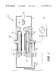
- FIG. 1 is a side section schematic view of a chamber suitable for performing PECVD according to embodiments of the invention
- FIG. 2 illustrates a graph of Ge content against RF power for devices manufactured according to embodiments of the invention
- FIG. 3 illustrates a graph of refractive index as a function of RF power for devices manufactured according to embodiments of the invention
- FIG. 4 illustrates a graph of change in refractive index for varying levels of RF power for samples constructed in accordance with the present invention
- FIG. 5 illustrates a graph of the measured P-etch rate for samples constructed in accordance wih the present invention
- FIG. 6 illustrates a schematic cross section of the construction of an alternative embodiment of the present invention
- FIGS. 7 a and 7 b illustrate graphs of change in refractive index for various levels of luminance for an alternative embodiment
- FIG. 8 illustrates a graph of relative birefringence for various levels of fluence for an alterntive embodiment of the present invention.
- a first embodiment of the present invention relies upon the utilisation of plasma enhanced chemical vapour deposition (PECVD).
- PECVD plasma enhanced chemical vapour deposition
- a vacuum chamber assembly 10 including a top electrode 11 and a bottom electrode 12 connected as shown to RF source 13 which comprised a 13.56 MHz RF source.
- RF source 13 which comprised a 13.56 MHz RF source.
- the chamber 14 is evacuated via pump port 15 and gases such as oxygen 16 , silane and germane 17 are introduced via corresponding ports so as to cause controlled deposition on wafers or substrates located in the RF field induced plasma located between electrodes 11 , 12 .
- a first wafer (W 1 ) 18 is mounted on top electrode 11 so as to be at a target potential.
- a second wafer 19 was also mounted near to but spaced apart from bottom electrode 12 .
- the spacing can be performed by ceramic supports 20 so as to electrically isolate wafer 19 .
- germanium doped silicon films produced by the PECVD process under the conditions specified resulted in the refractive index of the films being selectively controlled by irradiation (typically with a laser) by UV radiation. Conditions can therefore be utilised to produce controlled changes in refractive index of an irradiated portion of a wafer relative to the non-irradiated portions of the wafer. Particular examples of this behaviour will not be described in more detail.
- Ge-doped silica films were deposited on 2 inch diameter silicon substrates utilising a high plasma density hollow cathode reactor from mixtures of silane (SiH 4 ), germane (GeH 4 ) and oxygen.
- a suitable dual opposing target hollow cathode reactor was constructed in accordance with the known design as described in: “Hollow Cathode Etching and Deposition”, Journal of Vacuum Science and Technology, 1988, A6 at pages 1837-1844.
- the film was deposited on one wafer 18 clamped in the “face down” position to the top electrode. In one run, however, two wafers were deposited simultaneously.
- the first wafer w 1 18 was clamped to the top electrode in the normal manner, while the second wafer w 2 19 , was placed on the bottom electrode, but supported slightly above it on three small ceramic spacers e.g. 20 .
- the purpose of the spacers was to reduce the level of ion bombardment on water w 2 by reducing its voltage from the bias voltage of the electrode 12 to a potential close to the floating potential of the RF plasma glow. The reduction of ion bombardment is believed to result in increased porosity in the films thereby increasing scattering losses.
- the presence of wafer w 2 20 also altered the deposition conditions of wafer w 1 18 so that the film properties of w 1 , with and without wafer w 2 were observably different.
- the OH content and bond structure of the deposited films were determined by Fourier Transform Infrared Spectroscopy (FTIR), and the Ge content by Wavelength Dispersive X-ray Spectroscopy (WDS).
- FTIR Fourier Transform Infrared Spectroscopy
- WDS Wavelength Dispersive X-ray Spectroscopy
- the degree of the film porosity was estimated by measuring its etching rate in standard “P-solution”.
- the film stress was also calculated from the substrate curvature, as measured by stylus profilometry.
- the deposited films were subsequently UV exposed using a 193 nm excimer laser with a fluence of 10 kJ/cm 2 .
- the film refractive index, both before and after UV exposure, was measured using the known prism coupling technique at 633 nm wavelength with measurement repeatability within ⁇ 0.00015.
- the points 30 , 31 and 32 represent values measured for a system 10 utilising a single wafer 18 and no secondary wafer 19 and RF power values of 300, 450 and 600 watts respectively.
- the points 35 and 36 represent values measured for a dual wafer system at 600 watts where point 35 represents the measured value for wafer w 1 18 and the point 36 represents the measured value for the wafer w 2 19 . It can be seen that both the Ge was found to decrease with power for the single wafer deposition. In the case of dual wafers w 1 and w 2 , the Ge content of each wafer was found to be about the same but it was found to be approximately 4 times higher then the case of single wafer deposition at the same power.
- FIG. 3 shows the measured film refractive index as a function of RP power.
- the points marked 30 - 36 represent the data for the two wafers w 1 and w 2 as described previously.
- the results for the single wafer case 30 - 32 show the refractive index decreasing with power.
- the refractive indices in the dual wafer case of both w 1 35 and w 2 36 are higher than the case of one wafer deposition 32 .
- the change in refractive index after UV irradiation is shown in FIG. 4 . Both increases 36 and decreases 35 in refractive index are observed for the two wafer case.
- FIG. 5 there is illustrated a graph of the measured P-etch rate for the various samples 30 - 36 . The measured results were found to confirm the above comments.
- FIG. 7 a there is illustrated the consequential change in UV induced refractive index for various levels of accumulative fluence (kJ per cm 2 ) for the case of 25 mol. % of GeO 2 . All measurements were taken utilising an energy density of exposure of 0.33 watts per cm 2 for all exposures except for the exposure 50 . It can be noted from FIG. 7 a that the change in refractive index was found to vary with the cumulative fluence from initial positive value to negative values as indicated.
- FIG. 7 b there is illustrated the 15 mol. % of GeO 2 case for various cumulative fluences. It can be seen in comparing FIGS. 7 a and 7 b that the levels of refractive index change exhibit a dependence on the level of GeO 2 in the sample. Again, the point 51 of FIG. 7 b was derived from a UV light energy density of 1.4 watts/cm 2 .
- FIGS. 7 a and 7 b illustrate that the absolute value of the refractive index change is dependent on the total fluence in addition to the TV power density. Further, larger refractive index changes have been observed for the higher Ge content sample thus implying its higher photosensitivity compared to the lower Ge content sample. Photosensitivity further appears to increase with Ge content.
- FIG. 7 a and FIG. 7 b were obtained for TE polarised light injected into the waveguide.
- the TE polarised light is where the electric field vector is parallel to the substrate.
- FIG. 8 there is illustrated the birefringence, being the difference between the refractive indices for TE and TM polarised light, with the TM electric filed vector being perpendicular to the substrate, as a function of fluence.
- the measured results comprising curve 60 being measured for a wafer having 25 mol. % GeO 2 and the curve 61 representing those values measured for a wafer having 15 mol. % GeO 2 . It can be seen that the birefringence was found to vary both with the cumulative fluence and the degree of concentration of GeO 2 .
Landscapes
- Chemical & Material Sciences (AREA)
- Engineering & Computer Science (AREA)
- Physics & Mathematics (AREA)
- Materials Engineering (AREA)
- General Chemical & Material Sciences (AREA)
- Chemical Kinetics & Catalysis (AREA)
- Mechanical Engineering (AREA)
- Metallurgy (AREA)
- Organic Chemistry (AREA)
- Microelectronics & Electronic Packaging (AREA)
- General Physics & Mathematics (AREA)
- Optics & Photonics (AREA)
- Plasma & Fusion (AREA)
- Inorganic Chemistry (AREA)
- Optical Integrated Circuits (AREA)
Abstract
There is disclosed a method of constructing photosensitive waveguides on silicon wafers through the utilization of a Plasma Enhanced Vapor Deposition (PECVD) system. The deposition is utilized to vary the refractive index of resulting structures when they have been subject to Ultra Violet (UV) post processing.
Description
The present invention relates to improvements in the control of refractive index of films on substrates, and, more particularly, to a method, apparatus and means of fabrication of photosensitive germanium-doped silica films which change their refractive index upon UV irradiation.
Even more particularly the present invention also relates to the fabrication of photosensitive Germanium-doped silica files using plasma enhanced chemical vapour deposition (PECVD).
Photosensitivity in germanosilicate optical-fibres was first observed over 15 years ago. However it was the demonstration UV-written gratings which revived interest in this area. This was followed by writing reflection gratings in the telecommunications window of 1550 nm. These results have stimulated major activity worldwide in this area because such grating devices have a potential major impact on future telecommunications systems.
By coupling UV photosensitivity with planar silica waveguide technology, a very wide range of devices becomes possible and a high degree of integration can be achieved, bringing the benefits of device stability and compactness not available in fibres.
However, prior known germanium doped planar structures have been formed by flame hydrolysis and need to be hydrogen loaded for up to 2 weeks to become reasonably photosensitive. The hydrogen loading introduces unwanted side effects, such as transient behaviour due to gas out diffusion and increased absorption at 1.5 μm. An alternative deposition technique, which is able to produce photosensitive films without hydrogen loading, is Plasma Enhanced Chemical Vapour Deposition (PECVD). A UV-induced positive refractive index change of 0.0025 has been reported for germanium-doped PECVD silica films without utilising hydrogen loading. These “positive” photosensitive Ge-doped films, however, are deposited by standard high pressure (>50 Pa) PECVD and suffer from a high scattering loss, which makes this material less suitable for the fabrication of planar waveguide devices.
There is therefore a general need for an improved form of silica waveguide which does not suffer, to the same degree, the aforementioned problems.
In accordance with a first aspect of the present invention there is provided a method of fabricating a photosensitive germanium-doped silica film of a wafer, substrate or the like which is adapted to change its refractive index by a predetermined magnitude and sign upon UV irradiation, said method comprising the selection of deposition conditions for plasma enhanced chemical vapour deposition (PECVD) that result in the formation of a non-porous film.
Preferably the PECVD process is operated so as to control the structure of said film and to produce a film which is adopted to increase its refractive index upon UV irradiation. Alternatively, PECVD process is controlled so as to produce a film which is adopted to decrease its refractive index upon UV irradiation.
The PECVD should be carried out with the level of ion bombardment on the film surface during the deposition necessary for the formation of non-porous silica. The value of the change in refractive index can be adjusted by separately or simultaneously varying the level of ion bombardment and/or the temperature of the wafer, substrate or the like or the level of dopants.
GeH4 can be used as source material for germanium doping and preferably the PECVD process is carried out in a high plasma density hollow cathode deposition system comprising two opposing RF powered electrodes which operate to produce a high density plasma between them due to an “electron mirror” effect. The electrode opposing the wafer holding electrode can be partly screed to produce advantageous effects. The wafer holding electrode can be partly screened with a thin solid round plate having a diameter less than the diameter of the electrode and placed parallel to it and separated from it by a distance smaller than half of the inter-electrode distance.
In a second aspect of the present invention there is provided a photosensitive germanium-doped silica film on a wafer, substrate or the like which is adapted to change its refractive index upon UV irradiation, said film formed by plasma enhanced chemical vapour deposition (PECVD) of the film.
Preferably the PECVD process is operated so as to control the structure of said film and to produce either an increase or decrease in refractive meter upon UV irradiation.
The PECVD process is preferably carried out with the level of ion bombardment on the film surface during the deposition necessary for the formation of non-porous silica and the value of the change in refractive index is adjusted by separately or simultaneously varying the level of ion bombardment and/or the temperature of said wafer, substrate or the like or additionally varying the level of germanium doping.
Preferably GeH4 is used as source material for germanium doping.
The PECVD process can be carried out in a high plasma density hollow cathode deposition system comprising two opposing RF powered electrodes which operate to produce a high density plasma between them due to an “electron mirror” effect. One electrode can be partially screened to produce advantageous effects.
The partial screening can be done with a thin solid round plate having a diameter less than the diameter of the electrode and placed parallel to it and separated from it by a distance smaller than half of the inter-electrode distance.
In yet another aspect of the invention there is provided a method of forming an optical signal processing element on a substrate according to the method described above.
In accordance with a further aspect of the present invention there is provided a method of fabricating a photosensitive germanium doped silica film on a substrate the film adapted to change its refractive index upon UV irradiation, the method comprising utilising a plasma enhanced chemical vapour deposition (PECVD) of said film utilising a level of bombardment of the substrate surface sufficient to cause the formation of substantially non-porous silica.
In accordance with a further aspect of the present invention there is provided a method of fabricating a photosensitive germanium doped silica film on a substrate which is adapted to change its refractive index upon UV radiation, said method comprising plasma enhanced chemical vapour deposition (PECVD) of said film utilising a hollow cathode deposition system.
Preferably, the degree of change in refractive index is determined by varying one or more of:
(a) the level of germanium doping
(b) the level of ion bombardment of said substrate
(c) the degree of UV irradiation of said substrate
The invention also has application in changing the refractive index in respect of one birefringent axis with respect to a second birefringent axis.
In accordance with a further aspect of the present invention there is provided an optical waveguide comprising a photosensitive germanium doped silica film on a substrate, said waveguide adapted to change its refractive index upon UV irradiation, said film being formed from substantially non-porous deposition of said film. The deposition can be via plasma enhanced deposition of said film utilising a hollow cathode deposition system and the degree of change in the refractive index is determined by variation of one or more of:
(a) the level of germanium doping
(b) the degree of UV irradiation of said substrate.
Notwithstanding any other forms which may fall within the scope of the present invention, preferred forms of the invention will now be described, by way of example only, with reference to the accompanying drawings in which:
FIG. 1 is a side section schematic view of a chamber suitable for performing PECVD according to embodiments of the invention;
FIG. 2 illustrates a graph of Ge content against RF power for devices manufactured according to embodiments of the invention;
FIG. 3 illustrates a graph of refractive index as a function of RF power for devices manufactured according to embodiments of the invention;
FIG. 4 illustrates a graph of change in refractive index for varying levels of RF power for samples constructed in accordance with the present invention;
FIG. 5 illustrates a graph of the measured P-etch rate for samples constructed in accordance wih the present invention;
FIG. 6 illustrates a schematic cross section of the construction of an alternative embodiment of the present invention;
FIGS. 7a and 7 b illustrate graphs of change in refractive index for various levels of luminance for an alternative embodiment; and
FIG. 8 illustrates a graph of relative birefringence for various levels of fluence for an alterntive embodiment of the present invention.
A first embodiment of the present invention relies upon the utilisation of plasma enhanced chemical vapour deposition (PECVD).
With reference to FIG. 1 there is shown a vacuum chamber assembly 10 including a top electrode 11 and a bottom electrode 12 connected as shown to RF source 13 which comprised a 13.56 MHz RF source. In use for the purposes PECVD, the chamber 14 is evacuated via pump port 15 and gases such as oxygen 16, silane and germane 17 are introduced via corresponding ports so as to cause controlled deposition on wafers or substrates located in the RF field induced plasma located between electrodes 11, 12.
In this instance a first wafer (W1) 18 is mounted on top electrode 11 so as to be at a target potential.
In alternative experiments a second wafer 19, denoted W2, was also mounted near to but spaced apart from bottom electrode 12. The spacing can be performed by ceramic supports 20 so as to electrically isolate wafer 19.
Subsequent utilisation of the PECVD process in the example hereinafter disclosed resulted in the substrates 19,20 coated with a germanium doped silica film. Examples which are described in more detail below of germanium doped silicon films produced by the PECVD process under the conditions specified resulted in the refractive index of the films being selectively controlled by irradiation (typically with a laser) by UV radiation. Conditions can therefore be utilised to produce controlled changes in refractive index of an irradiated portion of a wafer relative to the non-irradiated portions of the wafer. Particular examples of this behaviour will not be described in more detail.
In a first example, Ge-doped silica films were deposited on 2 inch diameter silicon substrates utilising a high plasma density hollow cathode reactor from mixtures of silane (SiH4), germane (GeH4) and oxygen. A suitable dual opposing target hollow cathode reactor was constructed in accordance with the known design as described in: “Hollow Cathode Etching and Deposition”, Journal of Vacuum Science and Technology, 1988, A6 at pages 1837-1844.
A series of deposition runs, with varying RF power densities, were carried out at a process pressure of 2 Pa and a GeH4 flow rate of 6 sccm. The SiH4 flow rate was fixed at 20 sccm and the O2 flow rate was determined to give a SiH4/O2 ratio of approximately 6. No electrode cooling was used. In most of the deposition runs the film was deposited on one wafer 18 clamped in the “face down” position to the top electrode. In one run, however, two wafers were deposited simultaneously. The first wafer w1 18, was clamped to the top electrode in the normal manner, while the second wafer w2 19, was placed on the bottom electrode, but supported slightly above it on three small ceramic spacers e.g. 20. The purpose of the spacers was to reduce the level of ion bombardment on water w2 by reducing its voltage from the bias voltage of the electrode 12 to a potential close to the floating potential of the RF plasma glow. The reduction of ion bombardment is believed to result in increased porosity in the films thereby increasing scattering losses. In practice it was found that the presence of wafer w2 20 also altered the deposition conditions of wafer w1 18 so that the film properties of w1, with and without wafer w2 were observably different.
The OH content and bond structure of the deposited films were determined by Fourier Transform Infrared Spectroscopy (FTIR), and the Ge content by Wavelength Dispersive X-ray Spectroscopy (WDS). The degree of the film porosity was estimated by measuring its etching rate in standard “P-solution”. The film stress was also calculated from the substrate curvature, as measured by stylus profilometry.
In initial experiments, the deposited films were subsequently UV exposed using a 193 nm excimer laser with a fluence of 10 kJ/cm2. The film refractive index, both before and after UV exposure, was measured using the known prism coupling technique at 633 nm wavelength with measurement repeatability within ±0.00015.
Referring now to FIG. 2, there is shown the Ge content in example films utilised, as a function of the RF power level. The points 30, 31 and 32 represent values measured for a system 10 utilising a single wafer 18 and no secondary wafer 19 and RF power values of 300, 450 and 600 watts respectively. The points 35 and 36 represent values measured for a dual wafer system at 600 watts where point 35 represents the measured value for wafer w1 18 and the point 36 represents the measured value for the wafer w2 19. It can be seen that both the Ge was found to decrease with power for the single wafer deposition. In the case of dual wafers w1 and w2, the Ge content of each wafer was found to be about the same but it was found to be approximately 4 times higher then the case of single wafer deposition at the same power.
FIG. 3 shows the measured film refractive index as a function of RP power. The points marked 30-36 represent the data for the two wafers w1 and w2 as described previously. The results for the single wafer case 30-32 show the refractive index decreasing with power. Also, for the same power level of 600W, the refractive indices in the dual wafer case of both w1 35 and w2 36 are higher than the case of one wafer deposition 32. The change in refractive index after UV irradiation is shown in FIG. 4. Both increases 36 and decreases 35 in refractive index are observed for the two wafer case. Those samples w1 35 placed directly on the electrodes, and thus subjected to ion bombardment during deposition, exhibited a negative refractive index change. It was found that the refractive index decrease for w1 35 (deposited simultaneously with w2 36) was of the order of −0.006. At the same time w2 36, which was separated from the electrode and was receiving decreased ion bombardment, exhibited a positive refractive index change after UV irradiation.
Subsequent scanning electron microscope (SEM) analysis of the silica surface of the wafers w1, w2 after etching in standard P-solution (HF(60%):HNO3(70%).30H2O) for samples deposited in the presence of, and in the absence of, ion bombardment respectively, showed a marked roughness of wafer sample surface for the wafer w2 not subjected to substantial ion bombardment. The roughness being consistent with the P-etch rate being approximately four times higher for the wafer w2 in comparison with the wafer w1. This is consistent with the wafers w2, deposited without ion bombardment, having a significantly higher degree of porosity.
In FIG. 5 there is illustrated a graph of the measured P-etch rate for the various samples 30-36. The measured results were found to confirm the above comments.
Further experiments were then carried out. In a second series of experiments, wafers were initially constructed in accordance with the cross section 40 as illustrated in FIG. 6 with the silica wafer 41 first having a 10 μm layer of SiO 2 42 laid down as an undoped silica buffer layer. Once layer 42 is prepared, a 3 μm Ge doped silica layer 43 was subsequently formed in accordance with the aforementioned technique. In a first series of experiments, the GeO2 content was controlled to be 15 mol. % and in a second series of experiments, the GeO2 content was found to be 25 mol. %. The samples were then UV irradiated at various levels and the results plotted. The UV light energy density projected on the surface was normally kept at 0.33 watts per cm2 for all exposures except one exposure where it was increased to 1.4 watts per cm2.
Referring now to FIG. 7a, there is illustrated the consequential change in UV induced refractive index for various levels of accumulative fluence (kJ per cm2) for the case of 25 mol. % of GeO2. All measurements were taken utilising an energy density of exposure of 0.33 watts per cm2 for all exposures except for the exposure 50. It can be noted from FIG. 7a that the change in refractive index was found to vary with the cumulative fluence from initial positive value to negative values as indicated.
Referring now to FIG. 7b, there is illustrated the 15 mol. % of GeO2 case for various cumulative fluences. It can be seen in comparing FIGS. 7a and 7 b that the levels of refractive index change exhibit a dependence on the level of GeO2 in the sample. Again, the point 51 of FIG. 7b was derived from a UV light energy density of 1.4 watts/cm2.
FIGS. 7a and 7 b illustrate that the absolute value of the refractive index change is dependent on the total fluence in addition to the TV power density. Further, larger refractive index changes have been observed for the higher Ge content sample thus implying its higher photosensitivity compared to the lower Ge content sample. Photosensitivity further appears to increase with Ge content.
The results of FIG. 7a and FIG. 7b were obtained for TE polarised light injected into the waveguide. The TE polarised light is where the electric field vector is parallel to the substrate. In FIG. 8, there is illustrated the birefringence, being the difference between the refractive indices for TE and TM polarised light, with the TM electric filed vector being perpendicular to the substrate, as a function of fluence. The measured results comprising curve 60 being measured for a wafer having 25 mol. % GeO2 and the curve 61 representing those values measured for a wafer having 15 mol. % GeO2. It can be seen that the birefringence was found to vary both with the cumulative fluence and the degree of concentration of GeO2.
In general, it is thought that the increase in RF power coupled into the discharge leads to an increase in both the wafer temperature and the level of ion bombardment on the film surface, due to the increase in both ion flux and average energy of ions impinging on the surface. Further, a simultaneous increase in the temperature of the wafer and the level of ion bombardment on the film surface causes a decrease in both the Ge content (and hence refractive index) and the OH content.
It would be appreciated by a person skilled in the art that numerous variations and/or modifications may be made to the present invention as shown in the specific embodiments without departing from the spirit or scope of the invention as broadly described. The methods presented can readily be utilised in the construction of waveguide structures having predetermined refractive index profiles in accordance with requirement. The present embodiments are, therefore, to be considered in all respects to be illustrative and not restrictive.
Claims (29)
1. A method of fabricating a photosensitive germanium-doped silica film on a substrate by plasma enhanced chemical vapour deposition (PECVD), said film being arranged to undergo a change in refractive index by a predetermined magnitude and sign upon UV irradiation, said method comprising:
performing the PECVD under deposition conditions that enable the film to form as a non-porous film and to undergo the change in refractive index.
2. A method as claimed in claim 1 , wherein the step of performing the PECVD includes employing a level of ion bombardment of the film surface during deposition to form the non-porous film.
3. A method as claimed in claim 2 , wherein GeH4 is used as a source material to dope the film with germanium.
4. A method as claimed in claim 2 , further comprising carrying out the PECVD process in a high plasma density hollow cathode deposition system comprising two opposing RF-powered electrodes which operate to produce a high density plasma between them due to an “electron mirror” effect.
5. A method as claimed in claim 1 wherein said film is germanium doped utilizing GeH4 as a source material.
6. A method as claimed in claim 1 wherein the PECVD process is carried out in a high plasma density hollow cathode deposition system comprising two opposing RF powered electrodes which operate to produce a high density plasma between them due to an “electron mirror” effect.
7. A method as claimed in claim 6 wherein the electrode opposing the wafer holding electrode is partly screened.
8. A method as claimed in claim 7 wherein said wafer holding electrode is partly screened with a thin solid round plate having a diameter less than the diameter of the electrode and placed parallel to it and separated from it by a distance smaller than half of the inter-electrode distance.
9. A method as claimed in claim 1 wherein said change in refractive index is in respect of one birefringent axis relative to a second birefringent axis.
10. A method of fabricating a photosensitive germanium-doped silica film on a substrate by plasma enhanced chemical vapour deposition (PECVD), said film being arranged to undergo a decrease in refractive index by a predetermined magnitude, said method comprising:
performing the PECVD under deposition conditions that enable the film to undergo the decrease in refractive index.
11. A method as claimed in claim 10 , wherein said decrease in refractive index is in respect of one birefringent axis relative to a second birefringent axis.
12. A method as claimed in claim 10 , wherein GeH4 is used as a source material to dope the film with germanium.
13. A method as claimed in claim 10 , further comprising carrying out the PECVD process in a high plasma density hollow cathode deposition system comprising two opposing RF-powered electrodes which operate to produce a high density plasma between them due to an “electron mirror” effect.
14. A photosensitive germanium-doped silica film on a wafer, substrate or the like which is adapted to change its refractive index upon UV irradiation, said film formed by plasma enhanced chemical vapour deposition (PECVD) of the film wherein deposition conditions of the PECVD are chosen in a manner such as to control the magnitude and sign oil the UV-induced refractive index change of the film, wherein the PECVD process is operated so as to control the structure of said film so as to form a film of non-porous silica.
15. A film as claimed in claim 14 wherein the deposition conditions of the PECVD are chosen in a manner such as to produce a film which is adapted to decrease its refractive index upon UV irradiation.
16. A film as claimed in claim 14 wherein a level of ion bombardment on the film surface during the deposition necessary for the formation of non-porous silica is chosen.
17. A film as claimed in claim 14 wherein a level of ion bombardment and/or the temperature of said wafer, substrate or the like are chosen separately or simultaneously in a manner such as to control the magnitude and sign of the refractive index change.
18. A film as claimed in claim 14 wherein said film is germanium doped utilizing GeH4 as a source material.
19. A film as claimed in claim 14 wherein the PECVD process is carried out in a high plasma density hollow cathode deposition system comprising two opposing RF powered electrodes which operate to produce a high density plasma between them due to an “electron mirror” effect.
20. A film as claimed in claim 19 , wherein an electrode opposing a substrate-holding electrode is partly screened.
21. A film as claimed in claim 19 , wherein a substrate-holding electrode is partly screened with a thin solid round plate having a diameter less than the diameter of the electrode and placed parallel to and separated from the substrate-holding electrode by a distance smaller than half of an inter-electrode distance.
22. A film as claimed in claim 14 wherein said film is capable of forming an optical signal processing element on said substrate.
23. A film as claimed in claim 14 wherein said change in refractive index is in respect of one birefringent axis of the film relative to a second birefringent axis of the film.
24. A method of fabricating a photosensitive germanium-doped silica film on a substrate by plasma enhanced chemical vapour deposition (PECVD) in a hollow cathode deposition system, said film being a arranged to undergo a change in refractive index by a predetermined magnitude and sign upon UV irradiation, the method comprising:
performing the PECVD under deposition conditions that enable the film to undergo the change in refractive index, wherein the predetermined magnitude of change in refractive index is produced by varying one or more of:
(a) the level of ion bombardment of said substrate; and
(b) the degree of UV irradiation of said substrate.
25. A method as claimed in claim 24 wherein the PECVD plasma is created by two opposing RF powered electrodes which operate to produce a high density plasma between them.
26. A method as claimed in claim 25 wherein one of said electrodes is partially screened.
27. A method as claimed in claim 25 wherein said substrate is substantially at the potential of a corresponding one of said electrodes.
28. A method as claimed in claim 25 wherein said substrate is substantially at the potential of said plasma.
29. A method as claimed in claim 24 wherein said change is in respect of one birefringent axis with respect to a second birefringent axis.
Applications Claiming Priority (3)
| Application Number | Priority Date | Filing Date | Title |
|---|---|---|---|
| AUPN5268 | 1995-09-07 | ||
| AUPN5268A AUPN526895A0 (en) | 1995-09-07 | 1995-09-07 | Improvements in control of refractive index |
| PCT/AU1996/000563 WO1997009645A1 (en) | 1995-09-07 | 1996-09-06 | A method and apparatus for the construction of photosensitive waveguides |
Publications (1)
| Publication Number | Publication Date |
|---|---|
| US6379873B1 true US6379873B1 (en) | 2002-04-30 |
Family
ID=3789597
Family Applications (1)
| Application Number | Title | Priority Date | Filing Date |
|---|---|---|---|
| US09/029,407 Expired - Fee Related US6379873B1 (en) | 1995-09-07 | 1996-09-06 | Method and apparatus for the construction of photosensitive waveguides |
Country Status (6)
| Country | Link |
|---|---|
| US (1) | US6379873B1 (en) |
| EP (1) | EP0871910A4 (en) |
| JP (1) | JP2000511149A (en) |
| AU (1) | AUPN526895A0 (en) |
| CA (1) | CA2231373A1 (en) |
| WO (1) | WO1997009645A1 (en) |
Cited By (2)
| Publication number | Priority date | Publication date | Assignee | Title |
|---|---|---|---|---|
| US6528338B2 (en) | 2001-03-13 | 2003-03-04 | Redfern Integrated Optics Pty Ltd | Silica-based optical device fabrication |
| US6768856B2 (en) * | 2001-02-09 | 2004-07-27 | Corning Incorporated | High germanium content waveguide materials |
Families Citing this family (2)
| Publication number | Priority date | Publication date | Assignee | Title |
|---|---|---|---|---|
| AUPP930799A0 (en) * | 1999-03-18 | 1999-04-15 | University Of Sydney, The | Optical planar waveguide device and method of its fabrication |
| WO2002073257A1 (en) * | 2001-03-13 | 2002-09-19 | Redfern Integrated Optics Pty Ltd | Silica-based optical device fabrication |
Citations (7)
| Publication number | Priority date | Publication date | Assignee | Title |
|---|---|---|---|---|
| US4339173A (en) * | 1975-09-08 | 1982-07-13 | Corning Glass Works | Optical waveguide containing P2 O5 and GeO2 |
| US4450787A (en) * | 1982-06-03 | 1984-05-29 | Rca Corporation | Glow discharge plasma deposition of thin films |
| EP0478984A1 (en) * | 1990-10-05 | 1992-04-08 | International Business Machines Corporation | Plasma enhanced chemical vapor processing system using hollow cathode effect |
| US5230753A (en) * | 1991-12-03 | 1993-07-27 | Princeton University | Photostable amorphous silicon-germanium alloys |
| AU3529295A (en) | 1994-09-23 | 1996-04-09 | British Telecommunications Public Limited Company | Planar waveguides |
| US5506925A (en) * | 1995-02-28 | 1996-04-09 | At&T Corp. | Radiolytic modification of birefringence in silica planar waveguide structures |
| US5701378A (en) * | 1995-07-04 | 1997-12-23 | Pirelli General Plc | Optical structures with two optical guidance paths |
-
1995
- 1995-09-07 AU AUPN5268A patent/AUPN526895A0/en not_active Abandoned
-
1996
- 1996-09-06 WO PCT/AU1996/000563 patent/WO1997009645A1/en not_active Application Discontinuation
- 1996-09-06 US US09/029,407 patent/US6379873B1/en not_active Expired - Fee Related
- 1996-09-06 CA CA002231373A patent/CA2231373A1/en not_active Abandoned
- 1996-09-06 EP EP96928290A patent/EP0871910A4/en not_active Withdrawn
- 1996-09-06 JP JP09510710A patent/JP2000511149A/en active Pending
Patent Citations (7)
| Publication number | Priority date | Publication date | Assignee | Title |
|---|---|---|---|---|
| US4339173A (en) * | 1975-09-08 | 1982-07-13 | Corning Glass Works | Optical waveguide containing P2 O5 and GeO2 |
| US4450787A (en) * | 1982-06-03 | 1984-05-29 | Rca Corporation | Glow discharge plasma deposition of thin films |
| EP0478984A1 (en) * | 1990-10-05 | 1992-04-08 | International Business Machines Corporation | Plasma enhanced chemical vapor processing system using hollow cathode effect |
| US5230753A (en) * | 1991-12-03 | 1993-07-27 | Princeton University | Photostable amorphous silicon-germanium alloys |
| AU3529295A (en) | 1994-09-23 | 1996-04-09 | British Telecommunications Public Limited Company | Planar waveguides |
| US5506925A (en) * | 1995-02-28 | 1996-04-09 | At&T Corp. | Radiolytic modification of birefringence in silica planar waveguide structures |
| US5701378A (en) * | 1995-07-04 | 1997-12-23 | Pirelli General Plc | Optical structures with two optical guidance paths |
Non-Patent Citations (4)
| Title |
|---|
| Hubner et al., Proc. SPIE-Int. Soc. Opt. Eng. 1996, vol. 2695, pp. 98-105, UV-Written Y-Splitter in Ge-Doped Silica. |
| International search report dated Nov. 27, 1997. |
| Kirk-Othmer Encyclopedia of Chemical Technology, vol. 23 (4th Ed.) Published by John Wiley & Sons, Inc. (1997). |
| Svalgaard et al, Electronics Letters, Aug. 18, 1994, vol. 30, No. 17, pp. 1401-1403, "Direct UV Writing of Buried Single Mode Channel Waveguides in Ge-Doped Silica Films".* * |
Cited By (2)
| Publication number | Priority date | Publication date | Assignee | Title |
|---|---|---|---|---|
| US6768856B2 (en) * | 2001-02-09 | 2004-07-27 | Corning Incorporated | High germanium content waveguide materials |
| US6528338B2 (en) | 2001-03-13 | 2003-03-04 | Redfern Integrated Optics Pty Ltd | Silica-based optical device fabrication |
Also Published As
| Publication number | Publication date |
|---|---|
| WO1997009645A1 (en) | 1997-03-13 |
| AUPN526895A0 (en) | 1995-09-28 |
| CA2231373A1 (en) | 1997-03-13 |
| JP2000511149A (en) | 2000-08-29 |
| EP0871910A1 (en) | 1998-10-21 |
| EP0871910A4 (en) | 2000-09-20 |
Similar Documents
| Publication | Publication Date | Title |
|---|---|---|
| US20020104821A1 (en) | Reactive ion etching of silica structures | |
| JPH11503840A (en) | Silica-based optical device and method for manufacturing optoelectronic device | |
| JP2003525834A (en) | Radiation transmitting thin film on glass article | |
| US5707692A (en) | Apparatus and method for processing a base substance using plasma and a magnetic field | |
| US6379873B1 (en) | Method and apparatus for the construction of photosensitive waveguides | |
| AU703977B2 (en) | A method and apparatus for the construction of photosensitive waveguides | |
| JP3199829B2 (en) | Manufacturing method of amorphous carbon film | |
| US6528338B2 (en) | Silica-based optical device fabrication | |
| DK172355B1 (en) | Process for the preparation of germanium doped glasses and use of the method | |
| Li et al. | Ge-doped SiO2 thin films produced by helicon activated reactive evaporation | |
| Syms et al. | Near-infrared channel waveguides formed by electron-beam irradiation of silica layers on silicon substrates | |
| Wosinski et al. | Amorphous silicon in nanophotonic technology | |
| Bazylenko et al. | Photosensitivity of Ge-doped silica films deposited in a PECVD hollow cathode reactor | |
| JP3971524B2 (en) | Manufacturing method of optical waveguide | |
| Storgaard-Larsen et al. | Nitrogen doped germania glasses with enhanced optical and mechanical properties | |
| Bulla et al. | Deposition and characterization of silica-based films by helicon-activated reactive evaporation applied to optical waveguide fabrication | |
| Bazylenko et al. | Mechanisms of UV-induced refractive index changes in PECVD silica | |
| JP3445559B2 (en) | Manufacturing method of amorphous carbon film | |
| John et al. | Fabrication and demonstration of a pure silica-core waveguide utilizing a density-based index contrast | |
| JPH09292541A (en) | Production of optical planar device | |
| Boswell et al. | Deposition of silicon dioxide films using the helicon diffusion reactor for integrated optics applications | |
| Ditchfield et al. | Nitrogen Doped Germania Glasses with Enhanced Optical and Mechanical Properties | |
| Luo | Development of an integrated photonic sensor for monitoring hazardous organics | |
| Chang et al. | Fabrication and Characterization of Er doped silicon-rich-silicon nitride (SRSN) microdisks | |
| Bazylenko et al. | Two Types of Photosensitivity Observed in Hollow Cathode PECVD Germanosilica Planar Waveguides. |
Legal Events
| Date | Code | Title | Description |
|---|---|---|---|
| AS | Assignment |
Owner name: UNISEARCH LIMITED, AUSTRALIA Free format text: ASSIGNMENT OF ASSIGNORS INTEREST;ASSIGNORS:BAZYLENKO, MICHAEL;GROSS, MARK;MOSS, DAVID;AND OTHERS;REEL/FRAME:009471/0052;SIGNING DATES FROM 19980303 TO 19980305 |
|
| CC | Certificate of correction | ||
| CC | Certificate of correction | ||
| FPAY | Fee payment |
Year of fee payment: 4 |
|
| REMI | Maintenance fee reminder mailed | ||
| LAPS | Lapse for failure to pay maintenance fees | ||
| STCH | Information on status: patent discontinuation |
Free format text: PATENT EXPIRED DUE TO NONPAYMENT OF MAINTENANCE FEES UNDER 37 CFR 1.362 |
|
| FP | Lapsed due to failure to pay maintenance fee |
Effective date: 20100430 |