US6376896B1 - Semiconductor device having thin film resistor and method of manufacturing the same - Google Patents
Semiconductor device having thin film resistor and method of manufacturing the same Download PDFInfo
- Publication number
- US6376896B1 US6376896B1 US09/323,506 US32350699A US6376896B1 US 6376896 B1 US6376896 B1 US 6376896B1 US 32350699 A US32350699 A US 32350699A US 6376896 B1 US6376896 B1 US 6376896B1
- Authority
- US
- United States
- Prior art keywords
- polycrystal silicon
- film
- resistor
- type
- semiconductor device
- Prior art date
- Legal status (The legal status is an assumption and is not a legal conclusion. Google has not performed a legal analysis and makes no representation as to the accuracy of the status listed.)
- Expired - Lifetime
Links
Images


Classifications
-
- H—ELECTRICITY
- H10—SEMICONDUCTOR DEVICES; ELECTRIC SOLID-STATE DEVICES NOT OTHERWISE PROVIDED FOR
- H10D—INORGANIC ELECTRIC SEMICONDUCTOR DEVICES
- H10D1/00—Resistors, capacitors or inductors
- H10D1/40—Resistors
- H10D1/47—Resistors having no potential barriers
-
- H—ELECTRICITY
- H10—SEMICONDUCTOR DEVICES; ELECTRIC SOLID-STATE DEVICES NOT OTHERWISE PROVIDED FOR
- H10D—INORGANIC ELECTRIC SEMICONDUCTOR DEVICES
- H10D84/00—Integrated devices formed in or on semiconductor substrates that comprise only semiconducting layers, e.g. on Si wafers or on GaAs-on-Si wafers
- H10D84/80—Integrated devices formed in or on semiconductor substrates that comprise only semiconducting layers, e.g. on Si wafers or on GaAs-on-Si wafers characterised by the integration of at least one component covered by groups H10D12/00 or H10D30/00, e.g. integration of IGFETs
- H10D84/811—Combinations of field-effect devices and one or more diodes, capacitors or resistors
Definitions
- the present invention relates to a semiconductor device and, in particular, to a semiconductor device having a ladder resistor circuit using a polycrystal silicon resistor and to a method of manufacturing such semiconductor device.
- the conventional ladder resistor circuit using the n-type polycrystal silicon resistor suffers from such a problem that an area occupied by the ladder resistor circuit is caused to increase because the circuit uses a means for lengthening length of the resistor for the purpose of reducing the divided voltage output error.
- the present invention has an object to provide a ladder resistor circuit which has small divided voltage output error and high accuracy which are not allowed by the conventional ladder resistor circuit using the n-type polycrystal silicon resistor, with a small occupied area.
- the main means applied by the semiconductor device according to the present invention in order to achieve the above-mentioned object is as follows.
- the impurities introduced into a polycrystal silicon resistor in a ladder resistor circuit using a polycrystal silicon resistor are of p-type.
- the p-type impurities introduced into the polycrystal silicon resistor are BF 2 .
- the p-type impurities introduced into the p-type polycrystal silicon resistor are boron.
- the structure is characterized in that the film thickness of the p-type polycrystal silicon resistor is from 500 to 1500 ⁇ .
- the semiconductor device is characterized in that the sheet resistance of the p-type polycrystal silicon resistor is from 1 k ⁇ / to 25 k ⁇ /.
- the semiconductor device is characterized in that the temperature coefficient of the p-type polycrystal silicon resistor is ⁇ 4000 ppm/° C. or lower.
- the semiconductor device is characterized in that the length of the p-type polycrystal silicon resistor is from 10 ⁇ m to 150 ⁇ m.
- a method of manufacturing a semiconductor device comprising the steps of: forming an oxide film on a semiconductor substrate; forming a polycrystal silicon film of 500 ⁇ to 1500 ⁇ in film thickness on the oxide film; doping the polycrystal silicon film region with p-type impurities; forming a region of the polycrystal silicon film by etching the polycrystal silicon film; doping a part of the polycrystal silicon film by 1 ⁇ 10 15 to 5 ⁇ 10 16 atom/cm 2 ; forming an intermediate insulation film on the oxide film and the polycrystal silicon film; defining contact holes in the polycrystal silicon film and the intermediate insulation film on the semiconductor substrate; and providing metal wirings in the contact holes.
- a method of manufacturing a semiconductor device comprising the steps of: forming an oxide film on a semiconductor substrate; forming a first polycrystal silicon film on the oxide film; doping the first polycrystal silicon film region with impurities; forming a region of the first polycrystal silicon film by etching the first polycrystal silicon film; forming an insulation film on the surface of the semiconductor substrate including the upper portion of the first polycrystal silicon film region; forming a second polycrystal silicon film of 500 ⁇ to 1500 ⁇ in film thickness on the insulation film; doping the second polycrystal silicon film with p-type impurities by 1 ⁇ 10 14 to 1 ⁇ 10 15 atom/cm 2 ; forming a region of the second polycrystal silicon film by etching the second polycrystal silicon film; doping a part of the region of the second polycrystal silicon film by 1 ⁇ 10 15 to 5 ⁇ 10 16 atom/cm 2 ; forming an intermediate insulation film on the oxide film and the
- the structure is characterized in that the insulation film comprises an oxide film of 300 ⁇ to 1000 ⁇ in film thickness.
- the insulation film comprises a laminated structure comprised of a thermal oxide film of 300 ⁇ to 700 ⁇ in film thickness, a nitride film of 200 ⁇ to 1000 ⁇ in film thickness and a thermal oxide film of 100 ⁇ or less in film thickness.
- a method of manufacturing a semiconductor device comprising the steps of: forming an oxide film on a semiconductor substrate; forming a first polycrystal silicon film on the oxide film; doping the first polycrystal silicon film region with impurities; forming a region of the first polycrystal silicon film by etching the first polycrystal silicon film; forming an insulation film on the surface of the semiconductor substrate including the upper portion of the first polycrystal silicon film region; forming a second polycrystal silicon film of 500 ⁇ to 1500 ⁇ in film thickness on the insulation film; doping the second polycrystal silicon film with p-type impurities by 1 ⁇ 10 14 to 1 ⁇ 10 15 atom/cm 2 ; forming a region of the second polycrystal silicon film by etching the second polycrystal silicon film; doping the second polycrystal silicon film structuring an n-type polycrystal silicon resistor with n-type impurities by 1 ⁇ 10 15 to 5 ⁇ 10 16 atom/cm 2 ; do
- the method of manufacturing a semiconductor device is characterized in that the n-type impurities with which the polycrystal silicon film region is doped are phosphorus.
- the method of manufacturing a semiconductor device is characterized in that the n-type impurities with which the polycrystal silicon film region is doped are arsenic.
- the method of manufacturing a semiconductor device is characterized in that the p-type impurities with which a part of the region of the second polycrystal silicon film structuring the high resistant element and the second polycrystal silicon film structuring the low resistant element are doped and the p-type impurities with which the diffused region of the MOS transistor having the p-type diffused region is doped are introduced simultaneously.
- the method of manufacturing a semiconductor device is characterized in that the n-type impurities with which the region of the second polycrystal silicon film structuring the n-type polycrystal silicon resistor and the n-type impurities with which the diffused region of the MOS transistor having the n-type diffused region is doped are introduced simultaneously.
- FIG. 1 is a circuit diagram showing a ladder resistor circuit in accordance with one embodiment of the semiconductor device of the present invention.
- FIG. 2 is a schematic sectional view showing a resistor element of a semiconductor device according to the present invention shown in FIG. 1 .
- FIG. 3 is a graph showing a relation between the lengths of polycrystal silicon resistors 1000 ⁇ in film thickness into which BF 2 is introduced in the p-type and phosphorus is introduced in the n-type, and the divided voltage output voltage error of the ladder resistor circuit made up of the respective polycrystal silicon resistors.
- FIG. 4 is a graph showing a relation between the impurity dose amount and the sheet resistance when the impurities are introduced into the polycrystal silicon of 1000 ⁇ in film thickness with the p-type impurities being BF 2 and the n-type impurities being phosphorus.
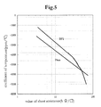
- FIG. 5 is a diagram showing a relation between the sheet resistance and the temperature coefficient when BF 2 is used as the p-type impurities and phosphorus is used as the n-type impurities in the polycrystal silicon of 1000 ⁇ in film thickness.
- FIG. 6 is a sectional view showing a process procedure of the method of manufacturing the resistor element in the semiconductor device of the present invention as shown in FIG. 1 .
- FIG. 7 is a cross-sectional view in the case where the present invention is applied to a semiconductor device including a MOS transistor and a capacitor.
- FIG. 8 is a sectional view showing a process procedure of the manufacturing method in the case where the present invention is applied to a semiconductor device including a MOS transistor and a capacitor.
- FIG. 9 is a sectional view showing a process procedure of a manufacturing method in the case where the present invention is applied to a semiconductor device including a polycrystal silicon resistor that constitutes a component other than the ladder circuit, a MOS transistor and a capacitor.
- FIG. 10 is a process diagram showing a completed product state in the case where the present invention is applied to a semiconductor device including a polycrystal silicon resistor that constitutes a component other than the ladder circuit, a MOS transistor and a capacitor.
- the semiconductor device can realize a ladder resistor circuit small in occupied area, small in divided voltage output error and high in accuracy by use of a polycrystal silicon resistor into which p-type impurities are introduced (hereinafter referred to as a p-type polycrystal silicon resistor).
- FIG. 1 is a circuit diagram showing a ladder resistor circuit in accordance with one embodiment of the semiconductor device of the present invention.
- a voltage V applied between a terminal A 11 and a terminal B 12 is divided by a resistor R 1 and a resistor R 2 to obtain a divided voltage V 0 from a terminal C 13 .
- the divided voltage V 0 is represented by the following expression.
- V 0 ( R 2 / R 1 + R 2 )* V (1)
- the divided voltage output error is represented by the following expression.
- the characteristic required for the polycrystal silicon resistor that constitutes the ladder circuit is that the divided voltage output error of the ladder circuit is small and the integrated area is also small.
- the polycrystal silicon film is thinned, because the variation in the concentration of the low-concentration impurities is reduced, the divided voltage output error of the ladder circuit becomes small, thereby being capable of producing a ladder circuit high in accuracy.
- the polycrystal silicon film is thinned, if the length of the polycrystal silicon resistor into which the impurities are introduced (hereinafter referred to as an n-type polycrystal silicon resistor) is shortened, the divided voltage output error is caused to increase, thereby making it difficult to reduce the integrated area.
- the p-type polycrystal silicon resistor is used, the length of that resistor is shortened so that the integrated area can be reduced. Its example will be described with reference to FIG. 3 .
- FIG. 3 is a graph showing a relation between the lengths of the p-type and n-type polycrystal silicon resistors each constituting a ladder circuit with 1000 ⁇ of film thickness and 10 k ⁇ / in sheet resistance and the divided voltage output error.
- An example is shown in which BF 2 ions are used as the p-type impurities introduced into the p-type polycrystal silicon resistor, and phosphorus is used as the n-type impurities introduced into the n-type polycrystal silicon resistor.
- the film thickness of the polycrystal silicon film of the ladder circuit made up of the n-type polycrystal silicon resistor is thinned to 1000 ⁇ , if the length of the polycrystal silicon resistor becomes 30 ⁇ m or less, the divided voltage output error of 0.5% or less cannot be ensured.
- the ladder circuit made up of the p-type polycrystal silicon resistor can ensure the divided voltage output error of 0.5% or less even if the length of the polycrystal silicon resistor is 10 ⁇ m.
- the divided voltage output error becomes small, which is effective.
- the film thickness of the polycrystal silicon film is thinned, the variation in the film thickness within the substrate and between the substrates increases, as a result of which the variation in the resistance increases. Accordingly, the divided voltage output error becomes large. For that reason, the film thickness is desirably 500 ⁇ to 1500 ⁇ , and its optimum value is 500 ⁇ . Also, as the length of the polycrystal silicon resistor is shortened, an influence of the grain size cannot be ignored, thereby increasing the variation in the resistance. For that reason, since the divided voltage output error increases, it is desirable that the length of the polycrystal silicon resistor is 10 ⁇ m or more, and also since the integrated area is caused to increase, 150 ⁇ m is the limit of polycrystal silicon resistor length.
- FIG. 4 is a graph showing a relation between the impurity dose amount and the sheet resistance when the impurities are introduced into the polycrystal silicon of 1000 ⁇ in film thickness through the ion implanting technique with the p-type impurities being BF 2 and the n-type impurities being phosphorus.
- the impurity dose amount varies “10% of the introduced impurity dose amount. Since the dose amount necessary for producing the polycrystal silicon resistor of 20 k ⁇ / in sheet resistance by using phosphorus is 3.5 ⁇ 10 14 atom/cm 2 , the dose amount varies to the degree of ⁇ 0.35 ⁇ 10 14 atom/cm 2 . That is, in the case where the polycrystal silicon resistor of 20 k ⁇ / in sheet resistance is to be produced by phosphorus, it is proved that the sheet resistance varies within the range of 13 k ⁇ / and 30 k ⁇ /.
- the dose amount necessary for producing the polycrystal silicon resistor of 20 k ⁇ / in sheet resistance by using BF 2 is 1.35 ⁇ 10 14 atom/cm 2
- the dose amount varies to the degree of ⁇ 0.135 ⁇ 10 14 atom/cm 2 . That is, in the case where the polycrystal silicon resistor of 20 k ⁇ / in sheet resistance is to be produced by BF 2 , the sheet resistance varies within the range of 17 k ⁇ / and 25 k ⁇ /. It is apparent from the above that BF 2 more reduces the variation in the concentration of the low concentration impurities as compared with phosphorus. As described above, if the variation in the concentration of the low concentration impurities is reduced, the divided voltage output error of the ladder circuit becomes small. That is, the ladder circuit made up of the p-type polycrystal silicon resistor can elevate the sheet resistance of the polycrystal silicon resistor while maintaining the divided voltage output error to 0.5% or less.
- the variation in the resistance to the temperature of the polycrystal silicon resistor which is of the p-type conductive type and about 5 k ⁇ / to 25 k ⁇ / in sheet resistance is about ⁇ 1700 ppm/° C. to ⁇ 4000 ppm/° C.
- the variation in resistance is smaller than that of the n-type polycrystal silicon resistor with the result that the oscillation frequency fluctuation can be reduced.
- the sheet resistance increases, the variation in the concentration of the low-concentration impurities increases, thereby making the divided voltage output error increase as described above.
- the sheet resistance is 25 k ⁇ / or less.
- the variation in the grain size cannot be ignored if the resistance is small, it is desirable that the sheet resistance is 1 k ⁇ / or more.
- the sheet resistance of the p-type polycrystal silicon resistor is 1 k ⁇ / to 25 k ⁇ / and the variation in the resistance to the temperature of the p-type polycrystal silicon resistor at that time is ⁇ 4000 ppm/° C. or less.
- FIG. 2 is a schematic sectional view showing one embodiment of a semiconductor device manufactured through the manufacturing method according to the present invention.
- FIG. 2 showing the sectional view of the resistant element used in the ladder resistor circuit of the present invention
- a high-resistant polycrystal silicon resistor 102 in the low-concentration impurity region into which BF 2 or as p-type impurities is introduced is formed on a silicon semiconductor substrate 101 through a field oxide film 103 .
- the film thickness of the polycrystal silicon film is 500 ⁇ TO 1500 ⁇ .
- a p-type high-concentration region 108 in which the concentration of the impurities is heightened so as to obtain sufficient contact with an aluminum wiring 105 is provided on both ends of the above resistor.
- a metal electrode 105 is disposed through the contact hole 21 in an intermediate insulation film 104 , on which a protective film 106 is disposed.
- FIG. 6 is a sectional view showing a process procedure of the manufacturing method shown in FIG. 2 in accordance with the present invention.
- FIG. 6 a shows an appearance in which the oxide film 103 is formed on the surface of the silicon substrate 11 , the polycrystal silicon film 102 is coated on the oxide film 103 through the CVD method (Chemical Vapor Deposition) or the sputtering method, and BF 2 which is the p-type impurities is introduced so as to obtain a desired sheet resistance through the ion implantation method.
- CVD method Chemical Vapor Deposition
- sputtering method BF 2 which is the p-type impurities
- the polycrystal silicon film 102 is set at 500 ⁇ to 1500 ⁇ in film thickness, and the p-type impurities BF 2 are introduced in the polycrystal silicon film 102 so as to obtain the sheet resistance of 1 k ⁇ / to 25 k ⁇ /.
- the p-type impurities introduced into the polycrystal silicon resistor 102 may be boron.
- the polycrystal silicon film is 1000 ⁇ in film thickness, and doped with BF 2 of about 1 ⁇ 10 14 to 1 ⁇ 10 15 atom/cm 2 which is the p-type impurities to obtain the sheet resistance of 1 k ⁇ / to 25 k ⁇ /.
- FIG. 6 b shows an appearance in which the polycrystal silicon resistor 102 is patterned through the photolithography method and the dry etching method. At this time, it is necessary that the length of the polycrystal silicon resistor is 10 ⁇ m to 150 ⁇ m.
- FIG. 6 c shows an appearance in which the photoresist 107 is patterned on the polycrystal silicon resistor 102 through the photolithography method in such a manner that a region which becomes the high-impurity concentration region 108 is opened in order to obtain sufficient contact with the aluminum wiring, and BF 2 which is the p-type impurities is introduced with the dose amount of 1 ⁇ 10 15 to 5 ⁇ 10 16 atom/cm 2 through the ion implantation method.
- BF 2 which is the p-type impurities is introduced with the dose amount of 5 ⁇ 10 15 atom/cm 2 in the high-impurity concentration region in order to obtain sufficient contact with the aluminum wiring of the polycrystal silicon resistor.
- FIG. 6 d shows an appearance of the p-type polycrystal silicon resistor 102 thus formed.
- the polycrystal silicon resistor that constitutes the components other than the ladder circuit may not always be made of the p-type polycrystal silicon. Taking the characteristics and the forming process into consideration, the type of polycrystal silicon may be selected. However, the p-type polycrystal silicon resistor is used on a portion requiring high accuracy.
- FIG. 7 is a cross-sectional view of the substrate in the case where the manufacturing method of the present invention is applied to the integrated circuit device including a MOS transistor and a capacitor.
- An n-type well region 210 which is opposite in conductivity to the p-type silicon semiconductor substrate is formed in a p-type silicon semiconductor substrate 201 .
- an n-type diffusion region 208 which is opposite in conductivity to the p-type silicon semiconductor substrate is formed on the p-type silicon semiconductor substrate 201
- a p-type diffusion region 209 which is opposite in conductivity to the well region is formed on the n-type well region 210 , thus forming a MOS transistor having a gate electrode 203 consisting of the respective diffusion layers and the first polycrystal silicon film.
- the p-type silicon semiconductor substrate is produced using the n-type silicon semiconductor substrate, the p-type transistor is produced in the n-type silicon semiconductor substrate, and the n-type transistor is produced in the p-type well region.
- the first polycrystal silicon film constitutes the gate electrode 203 and is formed on a field oxide film 202 as a capacitor electrode 204 .
- a capacitor electrode 207 formed of a second polycrystal silicon resistor into which BF 2 or boron is introduced is formed on the capacitor electrode 204 formed of the first polycrystal silicon film through an insulation film 205 .
- the second polycrystal silicon resistor forms a resistor 206 of the present invention which forms the capacitor electrode 207 and the ladder circuit.
- the gate electrode of FIG. 7 may be made of the second polycrystal silicon.
- the film thickness of the second polycrystal silicon is set at 4000 ⁇
- the film thickness of the second polycrystal silicon is set at 1000 ⁇ .
- FIG. 8 is a sectional view showing a process procedure of the substrate in the case where the manufacturing method of the present invention is applied to the integrated circuit device including a MOS transistor and a capacitor.
- FIG. 8 a shows an appearance in which after a silicon nitride film (Si 9 N 4 ) is patterned on the p-type semiconductor substrate 201 so as to open the n-type well region 210 which is opposite in conductivity to the p-type semiconductor substrate, the surface is doped with phosphorus which is the n-type impurities through the ion implantation method, thus removing the silicon nitride film. Then, the figure shows an appearance in which a separation region and an active region are formed through the Locos method.
- a silicon nitride film Si 9 N 4
- FIG. 8 b after the gate insulation film having, for example, a thickness of 300 ⁇ , has been formed through the thermal oxidizing method, the first polycrystal silicon film which will form the gate electrode 203 and the capacitor electrode 204 is coated on the oxide film through the CVD method or the sputtering method, and doped with phosphorus of high concentration through the ion implantation method or in an impurity diffusion furnace.
- FIG. 8 b shows an appearance in which the gate electrode 203 and the first polycrystal silicon resistor as the capacitor electrode 204 are patterned through the photolithography technique and the dry etching method.
- the film thickness of the gate insulation film is set at about 3 MV/cm.
- the power voltage of which is 30 V the oxide film of 1000 ⁇ or more in film thickness is required.
- FIG. 8 c shows an appearance in which the oxide film 205 which is 100 ⁇ to 300 ⁇ in film thickness is formed on the first polycrystal silicon film, a second polycrystal silicon which will form a second polycrystal silicon resistor 206 and the capacitor electrode 207 is coated on the upper surface through the CVD method or the sputtering method, and doped with BF 2 which is the p-type impurities through the ion implantation method.
- the second polycrystal silicon film is 500 ⁇ to 1500 ⁇ in film thickness and is doped with the p-type impurities of BF 2 to obtain the sheet resistance of 1 k ⁇ / to 25 k ⁇ /.
- the p-type impurities introduced into the polycrystal silicon resistor may be boron.
- the insulation film 205 on the first polycrystal silicon film as the capacitor electrode 204 may be an insulation film which is a laminated structure consisting of, for example, a thermal oxide film (Bottom.Ox) of 300 ⁇ in film thickness, a nitride film 500 ⁇ in film thickness produced through the CVD method and a thermal oxide film (Top. Ox) of about 10 ⁇ in film thickness, for the purpose of forming a high-quality capacitor, other than the thermal oxide film.
- the film thickness of the Bottom. Ox is set at about 300 ⁇ to 700 ⁇
- the film thickness of the nitride film is set at about 200 ⁇ to 1000 ⁇
- the film thickness of the Top. Ox is set at 100 ⁇ or less. It is preferable that the film thickness of the Bottom. Ox and the nitride film is determined according to a required breakdown field.
- FIG. 8 d shows an appearance in which the second polycrystal silicon resistors 206 and 207 are patterned through the photolithography method and the dry etching method. At this time, it is necessary that the length of the polycrystal silicon resistor is 10 ⁇ m to 150 ⁇ m.
- FIG. 8 e shows an appearance in which the photoresist is patterned through the photolithography method in such a manner that a region which becomes the diffusion region 208 of the n-type transistor is opened, and after arsenic which is the n-type impurities is introduced with the dose amount of 3 ⁇ 10 15 to 5 ⁇ 10 19 atom/cm 2 through the ion implantation method, a high-temperature heat treatment is conducted to activate and diffuse the implanted impurities.
- the photoresist 107 is patterned on the polycrystal silicon resistor through the photolithography method in such a manner that a region which will form a p-type high-impurity concentration region 211 and a region which will form the diffusion region 209 of the p-type transistor are opened in order to obtain sufficient contact with an aluminum wiring, thus introducing BF 2 of the p-type impurities through the ion implantation method.
- BF 2 which is the p-type impurities is introduced with the dose amount of 5 ⁇ 10 15 atom/cm 2 in the high-impurity concentration region 211 in order to obtain sufficient contact with the aluminum wiring of the polycrystal silicon resistor.
- FIG. 7 shows an appearance of the p-type polycrystal silicon resistor thus formed.
- the gate electrode shown in FIG. 8 c may be made of the second polycrystal silicon. Also, it is unnecessary to make the second polycrystal silicon equal in film thickness to the first polycrystal silicon, and the resistance can be arbitrarily set according to the film thickness of the polycrystal silicon. For example, the film thickness of the first polycrystal silicon may be set at 4000 ⁇ , and the film thickness of the second polycrystal silicon may be set at 1000 ⁇ .
- FIG. 9 is a sectional view showing a process procedure of the substrate in the case where the manufacturing method of the present invention is applied to the integrated circuit device including a resistor element other than a MOS transistor a capacitor, and a ladder circuit. The processes up to FIG.
- the photoresist is patterned through the photolithography method in such a manner that a region which will form the diffusion region 208 of the n-type transistor and a region which will form an n-type polycrystal silicon resistor 216 are opened, and after arsenic which is the n-type impurities is introduced with the dose amount of 3 ⁇ 10 15 to 5 ⁇ 10 19 atom/cm 2 through the ion implantation method, a high-temperature heat treatment is conducted to activate and diffuse the implanted impurities.
- the photoresist 107 is patterned on the polycrystal silicon resistor through the photolithography method in such a manner that a region which will form the p-type high-impurity concentration region 211 and a region which will form the diffusion region 209 of the p-type transistor are opened in order to obtain sufficient contact with an aluminum wiring, thus introducing BF 2 of the p-type impurities through the ion implantation method.
- BF 2 which is the p-type impurities is introduced with the dose amount of 5 ⁇ 10 15 atom/cm 2 in the high-impurity concentration region 211 in order to obtain sufficient contact with the aluminum wiring of the polycrystal silicon resistor.
- FIG. 10 shows an appearance of three kinds of polycrystal silicon resistor thus formed which are different in sheet resistance.
- the polycrystal silicon resistors 213 , 215 and 216 constituting the ladder circuit may be used for the polycrystal silicon resistor that constitutes a component other than the ladder circuit.
- Ar is ion-implanted with the dose amount of 1E14 to 1E16 atom/cm 2 subsequent to FIG. 8 d .
- the following precesses are identical with FIGS. 9 (A), 9 (B) and FIG. 10 in the stated order.
- the ion-implantation of Ar damages the polycrystal silicon film, and the grain size becomes small with the result that the grain boundaries increase.
- the sheet resistance of the n-type polycrystal silicon resistor into which n-type ions segregated by the grain boundaries are implanted is heightened, but the sheet resistance of the p-type polycrystal silicon resistor into which p-type ions not segregated by the grain boundaries are implanted is not changed. In this way, the sheet resistance of the n-type polycrystal silicon resistor can be changed by changing the doze amount of Ar which is ion-implanted.
- the sheet resistance is higher as compared with the prior art, the length is shortened, and a state in which the temperature coefficient is small can be produced.
- the ladder resistor circuit which is short in the length of the resistor and small in the divided voltage output error can be obtained which could not be obtained by the conventional ladder resistor circuit using the n-type polycrystal silicon resistor. Consequently, a high-accuracy ladder resistor circuit can be realized with a small occupied area, the costs can be reduced and the ladder resistor circuit is applicable to an IC, the chip size of which is restricted. Thus, great advantages can be obtained in many ICs.
Landscapes
- Semiconductor Integrated Circuits (AREA)
Abstract
Description
Claims (5)
Priority Applications (2)
| Application Number | Priority Date | Filing Date | Title |
|---|---|---|---|
| JP11101669A JP2000058755A (en) | 1998-06-02 | 1999-04-08 | Semiconductor device and manufacture of it |
| US09/323,506 US6376896B1 (en) | 1999-04-08 | 1999-06-01 | Semiconductor device having thin film resistor and method of manufacturing the same |
Applications Claiming Priority (2)
| Application Number | Priority Date | Filing Date | Title |
|---|---|---|---|
| JP11101669A JP2000058755A (en) | 1998-06-02 | 1999-04-08 | Semiconductor device and manufacture of it |
| US09/323,506 US6376896B1 (en) | 1999-04-08 | 1999-06-01 | Semiconductor device having thin film resistor and method of manufacturing the same |
Publications (1)
| Publication Number | Publication Date |
|---|---|
| US6376896B1 true US6376896B1 (en) | 2002-04-23 |
Family
ID=26442507
Family Applications (1)
| Application Number | Title | Priority Date | Filing Date |
|---|---|---|---|
| US09/323,506 Expired - Lifetime US6376896B1 (en) | 1998-06-02 | 1999-06-01 | Semiconductor device having thin film resistor and method of manufacturing the same |
Country Status (1)
| Country | Link |
|---|---|
| US (1) | US6376896B1 (en) |
Cited By (3)
| Publication number | Priority date | Publication date | Assignee | Title |
|---|---|---|---|---|
| US6727556B2 (en) * | 2000-08-09 | 2004-04-27 | Seiko Instruments Inc. | Semiconductor device and a method of manufacturing thereof |
| US20060166454A1 (en) * | 2005-01-27 | 2006-07-27 | International Business Machines Corporation | Low tolerance polysilicon resistor for low temperature silicide processing |
| US20110050660A1 (en) * | 2009-09-02 | 2011-03-03 | Kwang-Min Kim | Organic Light Emitting Display Device |
Citations (7)
| Publication number | Priority date | Publication date | Assignee | Title |
|---|---|---|---|---|
| US4210996A (en) * | 1977-05-04 | 1980-07-08 | Nippon Telegraph And Telephone Public Corporation | Trimming method for resistance value of polycrystalline silicon resistors especially used as semiconductor integrated circuit resistors |
| US4496935A (en) * | 1982-02-12 | 1985-01-29 | Matsushita Electric Industrial Co., Ltd. | Analog-digital converter with linear characteristic restoration circuit |
| US5128731A (en) * | 1990-06-13 | 1992-07-07 | Integrated Device Technology, Inc. | Static random access memory cell using a P/N-MOS transistors |
| US5235312A (en) * | 1991-11-18 | 1993-08-10 | Micron Technology, Inc. | Polysilicon resistors and methods of fabrication |
| US5554989A (en) * | 1993-08-06 | 1996-09-10 | Mitsubishi Denki Kabushiki Kaisha | A/D converter having folded arrangement of voltage comparator |
| US5554873A (en) * | 1994-05-23 | 1996-09-10 | Texas Instruments Incorporated | Semiconductor device having polysilicon resistor with low temperature coefficient |
| US5666007A (en) * | 1994-05-09 | 1997-09-09 | National Semiconductor Corporation | Interconnect structures for integrated circuits |
-
1999
- 1999-06-01 US US09/323,506 patent/US6376896B1/en not_active Expired - Lifetime
Patent Citations (7)
| Publication number | Priority date | Publication date | Assignee | Title |
|---|---|---|---|---|
| US4210996A (en) * | 1977-05-04 | 1980-07-08 | Nippon Telegraph And Telephone Public Corporation | Trimming method for resistance value of polycrystalline silicon resistors especially used as semiconductor integrated circuit resistors |
| US4496935A (en) * | 1982-02-12 | 1985-01-29 | Matsushita Electric Industrial Co., Ltd. | Analog-digital converter with linear characteristic restoration circuit |
| US5128731A (en) * | 1990-06-13 | 1992-07-07 | Integrated Device Technology, Inc. | Static random access memory cell using a P/N-MOS transistors |
| US5235312A (en) * | 1991-11-18 | 1993-08-10 | Micron Technology, Inc. | Polysilicon resistors and methods of fabrication |
| US5554989A (en) * | 1993-08-06 | 1996-09-10 | Mitsubishi Denki Kabushiki Kaisha | A/D converter having folded arrangement of voltage comparator |
| US5666007A (en) * | 1994-05-09 | 1997-09-09 | National Semiconductor Corporation | Interconnect structures for integrated circuits |
| US5554873A (en) * | 1994-05-23 | 1996-09-10 | Texas Instruments Incorporated | Semiconductor device having polysilicon resistor with low temperature coefficient |
Cited By (7)
| Publication number | Priority date | Publication date | Assignee | Title |
|---|---|---|---|---|
| US6727556B2 (en) * | 2000-08-09 | 2004-04-27 | Seiko Instruments Inc. | Semiconductor device and a method of manufacturing thereof |
| KR100899489B1 (en) * | 2000-08-09 | 2009-05-27 | 세이코 인스트루 가부시키가이샤 | Semiconductor device and a method of manufacturing thereof |
| US20060166454A1 (en) * | 2005-01-27 | 2006-07-27 | International Business Machines Corporation | Low tolerance polysilicon resistor for low temperature silicide processing |
| US7285472B2 (en) * | 2005-01-27 | 2007-10-23 | International Business Machines Corporation | Low tolerance polysilicon resistor for low temperature silicide processing |
| CN100388463C (en) * | 2005-01-27 | 2008-05-14 | 国际商业机器公司 | Method for manufacturing precision silicon-containing resistor |
| US20110050660A1 (en) * | 2009-09-02 | 2011-03-03 | Kwang-Min Kim | Organic Light Emitting Display Device |
| US8742784B2 (en) | 2009-09-02 | 2014-06-03 | Samsung Display Co., Ltd. | Organic light emitting display device |
Similar Documents
| Publication | Publication Date | Title |
|---|---|---|
| US4965220A (en) | Method of manufacturing a semiconductor integrated circuit device comprising an MOS transistor and a bipolar transistor | |
| US6110772A (en) | Semiconductor integrated circuit and manufacturing method thereof | |
| US5465005A (en) | Polysilicon resistor structure including polysilicon contacts | |
| US4697332A (en) | Method of making tri-well CMOS by self-aligned process | |
| US5393691A (en) | Fabrication of w-polycide-to-poly capacitors with high linearity | |
| US4845532A (en) | Semiconductor devices | |
| KR100251882B1 (en) | Gigaohm Load Resistors for BICMOS Processes | |
| US6653694B1 (en) | Reference voltage semiconductor | |
| US20020084492A1 (en) | Complementary MOS semiconductor device and method of manufacturing the same | |
| US4797372A (en) | Method of making a merge bipolar and complementary metal oxide semiconductor transistor device | |
| US5759887A (en) | Semiconductor device and a method of manufacturing a semiconductor device | |
| US5316960A (en) | C-MOS thin film transistor device manufacturing method | |
| KR960006104B1 (en) | Semiconductor integrated circuit device and manufacturing method thereof | |
| US4965216A (en) | Method of fabricating a bi-CMOS device | |
| WO1990016081A1 (en) | HIGH DENSITY BiCMOS CIRCUITS AND METHODS OF MAKING SAME | |
| KR0178551B1 (en) | Method of manufacturing semiconductor integrated circuit | |
| EP0151347B1 (en) | Integrated circuit having bipolar and field effect devices and method of fabrication | |
| US5691226A (en) | Method of manufacturing BICMOS integrated circuits | |
| US6376896B1 (en) | Semiconductor device having thin film resistor and method of manufacturing the same | |
| KR920010316B1 (en) | Manufacturing method of semiconductor device | |
| US6984869B2 (en) | High performance diode implanted voltage controlled p-type diffusion resistor | |
| JP3054937B2 (en) | Semiconductor device and manufacturing method thereof | |
| JPH11297847A (en) | Semiconductor device and manufacturing method thereof | |
| GB2212327A (en) | Polysilicon emitter transistor fabrication | |
| US6479338B2 (en) | CMOS device and method of manufacturing the same |
Legal Events
| Date | Code | Title | Description |
|---|---|---|---|
| AS | Assignment |
Owner name: SEIKO INSTRUMENTS INC., JAPAN Free format text: ASSIGNMENT OF ASSIGNORS INTEREST;ASSIGNORS:SHIIKI, MIKA;OSANAI, JUN;REEL/FRAME:012502/0475 Effective date: 20011115 |
|
| STCF | Information on status: patent grant |
Free format text: PATENTED CASE |
|
| FPAY | Fee payment |
Year of fee payment: 4 |
|
| FPAY | Fee payment |
Year of fee payment: 8 |
|
| FPAY | Fee payment |
Year of fee payment: 12 |
|
| AS | Assignment |
Owner name: SII SEMICONDUCTOR CORPORATION, JAPAN Free format text: ASSIGNMENT OF ASSIGNORS INTEREST;ASSIGNOR:SEIKO INSTRUMENTS INC.;REEL/FRAME:038058/0892 Effective date: 20160105 |
|
| AS | Assignment |
Owner name: ABLIC INC., JAPAN Free format text: CHANGE OF NAME;ASSIGNOR:SII SEMICONDUCTOR CORPORATION;REEL/FRAME:045567/0927 Effective date: 20180105 |