US6368971B2 - Method of manufacturing bottom electrode of capacitor - Google Patents

Method of manufacturing bottom electrode of capacitor Download PDF

Info

Publication number
US6368971B2
US6368971B2 US09/348,408 US34840899A US6368971B2 US 6368971 B2 US6368971 B2 US 6368971B2 US 34840899 A US34840899 A US 34840899A US 6368971 B2 US6368971 B2 US 6368971B2
Authority
US
United States
Prior art keywords
dielectric layer
forming
layer
trench
node contact
Prior art date
Legal status (The legal status is an assumption and is not a legal conclusion. Google has not performed a legal analysis and makes no representation as to the accuracy of the status listed.)
Expired - Fee Related
Application number
US09/348,408
Other versions
US20010003674A1 (en
Inventor
Sun-Chieh Chien
Chien-Li Kuo
Wei-Wu Liao
Current Assignee (The listed assignees may be inaccurate. Google has not performed a legal analysis and makes no representation or warranty as to the accuracy of the list.)
United Microelectronics Corp
Original Assignee
United Microelectronics Corp
Priority date (The priority date is an assumption and is not a legal conclusion. Google has not performed a legal analysis and makes no representation as to the accuracy of the date listed.)
Filing date
Publication date
Application filed by United Microelectronics Corp filed Critical United Microelectronics Corp
Priority to US09/348,408 priority Critical patent/US6368971B2/en
Assigned to UNITED SILICON INCORPORATED, UNITED MICROELECTRONICS CORP. reassignment UNITED SILICON INCORPORATED ASSIGNMENT OF ASSIGNORS INTEREST (SEE DOCUMENT FOR DETAILS). Assignors: LIAO, WEI-WU, KUO, CHIEN-LI, CHIEN, SUN-CHIEH
Assigned to UNITED MICROELECTRONICS CORP. reassignment UNITED MICROELECTRONICS CORP. ASSIGNMENT OF ASSIGNORS INTEREST (SEE DOCUMENT FOR DETAILS). Assignors: UNITED SILICON INCORPORATED
Publication of US20010003674A1 publication Critical patent/US20010003674A1/en
Application granted granted Critical
Publication of US6368971B2 publication Critical patent/US6368971B2/en
Anticipated expiration legal-status Critical
Expired - Fee Related legal-status Critical Current

Links

Images

Classifications

    • HELECTRICITY
    • H01ELECTRIC ELEMENTS
    • H01LSEMICONDUCTOR DEVICES NOT COVERED BY CLASS H10
    • H01L28/00Passive two-terminal components without a potential-jump or surface barrier for integrated circuits; Details thereof; Multistep manufacturing processes therefor
    • H01L28/40Capacitors
    • H01L28/60Electrodes
    • H01L28/82Electrodes with an enlarged surface, e.g. formed by texturisation
    • H01L28/90Electrodes with an enlarged surface, e.g. formed by texturisation having vertical extensions
    • H01L28/91Electrodes with an enlarged surface, e.g. formed by texturisation having vertical extensions made by depositing layers, e.g. by depositing alternating conductive and insulating layers
    • HELECTRICITY
    • H10SEMICONDUCTOR DEVICES; ELECTRIC SOLID-STATE DEVICES NOT OTHERWISE PROVIDED FOR
    • H10BELECTRONIC MEMORY DEVICES
    • H10B12/00Dynamic random access memory [DRAM] devices
    • H10B12/30DRAM devices comprising one-transistor - one-capacitor [1T-1C] memory cells
    • H10B12/31DRAM devices comprising one-transistor - one-capacitor [1T-1C] memory cells having a storage electrode stacked over the transistor
    • H10B12/315DRAM devices comprising one-transistor - one-capacitor [1T-1C] memory cells having a storage electrode stacked over the transistor with the capacitor higher than a bit line

Definitions

  • FIGS. 2A through 2E are schematic, cross-sectional views of the process for manufacturing a bottom electrode of a capacitor in a preferred embodiment according to the invention.

Landscapes

  • Engineering & Computer Science (AREA)
  • Power Engineering (AREA)
  • Computer Hardware Design (AREA)
  • Microelectronics & Electronic Packaging (AREA)
  • Semiconductor Memories (AREA)
  • Internal Circuitry In Semiconductor Integrated Circuit Devices (AREA)

Abstract

A method of manufacturing a bottom electrode of a capacitor. A substrate has a contact pad formed thereon, a first dielectric layer is formed on the contact pad, and a node contact penetrates through the first dielectric layer and electrically couples to the contact pad. A second dielectric layer is formed on the first dielectric layer and the node contact. A third dielectric layer is formed on the second dielectric layer. A fourth dielectric layer is formed on the third dielectric layer. A trench is formed to penetrate through the fourth, the third and the second dielectric layer and to expose a surface of the node contact. A conductive layer is formed on the fourth dielectric layer and a sidewall and a bottom of the trench. A fifth dielectric layer is formed on the conductive layer, wherein the fifth dielectric layer fills the trench. A portion of the fifth dielectric layer and a portion of the conductive layer are removed until a surface of the fourth dielectric layer is exposed. The remaining fifth dielectric layer and the fourth dielectric layer are removed.

Description

BACKGROUND OF THE INVENTION
1. Field of Invention
The present invention relates to a method of manufacturing a semiconductor device. More particularly, the present invention relates to a method of manufacturing a bottom electrode of a capacitor.
2. Description of Related Art
Dynamic random access memory (DRAM) is applied broadly in the field of integrated circuits devices, and more importantly, in the electronics industry. DRAMs with higher capacitance are necessary for the development of the industry. In order to simplify the circuit constitution and to increase the density of the device, the conventional memory cell composed of three transistors is replaced by a current memory cell which is composed of a transistor series-coupled to a capacitor.
The capacitor is used to store charges that are digital data. The more the capacitance is, the less the loss of digital data is. In addition to increasing the dielectric constant of the capacitor dielectric layer and decreasing the thickness of the capacitor dielectric layer, the area of the capacitor is increased to enhance the capacitance.
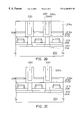
FIG. 1A is schematic, cross-sectional view of a conventional bottom electrode of a DRAM capacitor. As shown in FIG. 1, the method of manufacturing a bottom electrode 114 comprises forming a dielectric layer 106 over a substrate 100 including a dielectric layer 102 and a contact pad 104. The contact pad 104 is electrically coupled to a source/drain region (not shown) formed in the substrate 100. After that, bit lines 108 and a dielectric layer 110 are formed on the dielectric layer 106 in sequence, wherein the dielectric layer 110 fills the spaces between the bit lines 108 and covers the bit lines 108. Thereafter, a photolithography and etching process is performed to define the dielectric layers 108 and 106 and to form a node contact hole 112. The node contact hole 112 penetrates through the dielectric layers 108 and 106 and exposes a portion of the contact pad 104. Then, a polysilicon layer (not shown) is formed over the substrate 100 and fills the node contact hole 112. After that, a portion of the polysilicon layer is removed until the surface of the dielectric layer 108 is exposed and a node contact 112 a is formed in the node contact hole 112. A polysilicon layer (not shown) is formed over the substrate 100. A polysilicon photolithography and etching process is performed to form a bottom electrode 114 electrically coupled to the contact pad 104 through the node contact 112 a.
Since it is difficult to control the polysilicon photolithography and etching process, polysilicon material easily remains on the surface of the dielectric layer 110, which leads to the problem of a short in the capacitor. Moreover, the cross-sectional area of the bottom electrode 114 decreases from the top of the bottom electrode 114 to the bottom of the bottom electrode 114 (as shown in FIG. 1) because the polysilicon photolithography and etching process is difficult to control. Therefore, the bottom electrode will collapse in the subsequent manufacturing process.
SUMMARY OF THE INVENTION
The invention provides a method of manufacturing a bottom electrode of a capacitor. A substrate is provided. The substrate has a contact pad formed thereon, a first dielectric layer formed on the contact pad, and a node contact penetrating through the first dielectric layer and electrically coupled to the contact pad. A second dielectric layer is formed on the first dielectric layer and the node contact. A third dielectric layer is formed on the second dielectric layer. A fourth dielectric layer is formed on the third dielectric layer. A trench is formed to penetrate through the fourth, the third and the second dielectric layer and to expose a surface of the node contact. A conductive layer is formed on the fourth dielectric layer and a sidewall and a bottom of the trench. A fifth dielectric layer is formed on the conductive layer, wherein the fifth dielectric layer fills the trench. A portion of the fifth dielectric layer and a portion of the conductive layer are removed until a surface of the fourth dielectric layer is exposed. The remaining fifth dielectric layer and the fourth dielectric layer are removed.
As embodied and broadly described herein, the invention provides a method of manufacturing a bottom electrode of a capacitor. Since the thickness of the fourth dielectric layer can be varied with the height of the bottom electrode, the structure of the bottom electrode is relatively firm. Therefore, the invention can overcome the problem of the bottom electrode collapsing. Incidentally, in the invention, because the trench is formed in the fourth dielectric layer before the conductive layer is formed, it is unnecessary to perform the polysilicon photolithography and etching process. Hence, the problem due to the difficult-to-control polysilicon photolithography and etching process can be overcome.
It is to be understood that both the foregoing general description and the following detailed description are exemplary, and are intended to provide further explanation of the invention as claimed.
BRIEF DESCRIPTION OF THE DRAWINGS
The accompanying drawings are included to provide a further understanding of the invention, and are incorporated in and constitute a part of this specification. The drawings illustrate embodiments of the invention and, together with the description, serve to explain the principles of the invention. In the drawings,
FIG. 1A is schematic, cross-sectional view of a conventional bottom electrode of a DRAM capacitor; and
FIGS. 2A through 2E are schematic, cross-sectional views of the process for manufacturing a bottom electrode of a capacitor in a preferred embodiment according to the invention.
DESCRIPTION OF THE PREFERRED EMBODIMENTS
FIGS. 2A through 2E are schematic, cross-sectional views of the process for manufacturing a bottom electrode of a capacitor in a preferred embodiment according to the invention.
As shown in FIG. 2A, a substrate 200 having semiconductor devices (not shown) formed therein is provided, wherein the semiconductor devices comprise isolation regions, source/drain region and gate structure. The substrate 200 further comprises a dielectric layer 202 including contact pads 204, a dielectric layer 206, bit lines 208 and a dielectric layer 210 filling the spaces between the bit lines 208. The contact pads 204 are electrically coupled to the source/drain region in the substrate 200. The dielectric layer 210 can be formed from silicon oxide by chemical vapor deposition, for example. A node contact hole 212 is formed to penetrate through the dielectric layers 210 and 206 and exposes a portion of the contact pad 204. A node contact 212 a is formed in the node contact hole 212 and fills the node contact hole 212. The node contact 212 a is electrically coupled to the source/drain region (not shown) through the contact pad 204. The method of forming the node contact 212 a comprises forming a conductive layer (not shown) over the substrate 200, wherein the conductive layer fills the node contact hole 212. A portion of the conductive layer is removed until the surface of the dielectric layer 210 is exposed. The method of removing a portion of the conductive layer can be chemical-mechanical polishing (CMP) or etching back, for example. The material of the node contact 212 a can be polysilicon, for example.
As shown in FIG. 2B, dielectric layers 214, 216 and 218 are formed on the dielectric layer 210 and the node contact 212 a in sequence. The dielectric layer 214 can be formed from silicon oxide by CVD. Preferably, the method of forming the dielectric layer 214 includes low pressure chemical vapor deposition (LPCVD) or plasma-enhanced chemical vapor deposition (PECVD). Moreover, the thickness of the dielectric layer 214 can be varied with the height of the subsequently formed bottom electrode. The dielectric layer 216 serves as a mask layer in subsequent etching process. Additionally, the dielectric layer 216 can be formed from silicon nitride by LPCVD or PECVD and the thickness of the dielectric layer 216 is about 200-500 angstroms, for example. Preferably, the thickness of the dielectric layer 216 is about 300 angstroms. Furthermore, the etching rate of the dielectric layer 218 is different from that of the dielectric layer 216, and the dielectric layer 218 can be formed from silicon oxide by CVD, for example. Preferably, the method of forming the dielectric layer 218 comprises LPCVD or PECVD.
As shown in FIG. 2C, the dielectric layers 218, 218 and 214 are patterned to form a trench 220 penetrating through the dielectric layers 218, 216 and 214. The dielectric layers 218, 216 and 214 penetrated through by the trench 220 are respectively denoted as dielectric layers 218 a, 216 a and 214 a. The trench 220 exposes the surface of the node contact 212 and a portion of the dielectric layer 210. A conductive layer 222 is formed on the dielectric layer 218 a, the sidewall and the bottom surface of the trench 220. The conductive layer 222 can be formed from polysilicon by CVD, for example. A dielectric layer 224 is formed on the conductive layer 222 and fills the trench 220. The dielectric layer 220 can be formed from silicon oxide by CVD, for example.
As shown in FIG. 2D, a portion of the conductive layer 222 and a portion of the dielectric layer 224 are removed until the surface of the dielectric layer 218 a is exposed. Hence, the remaining conductive layer 222 and the remaining dielectric layer 224 are respectively denoted as a conductive layer 222 a and a dielectric layer 224 a. The method of removing the portion of the conductive layer 222 and the portion of the dielectric layer 224 can be CMP or etching back, for example.
As shown in FIG. 2E, the dielectric layers 218 a and 224 a are removed, with the dielectric layer 216 a serving as a mask layer, until a portion of the conductive layer 220 a located at the bottom of the trench 220 is exposed. The conductive layer 222 a forms a crown-type bottom electrode of a capacitor. The crown-type bottom electrode is electrically coupled to the source/drain region in the substrate 200 through the node contact 212 and contact pad 204. The method of removing the dielectric layers 218 a and 224 a can be dry etching or wet etching, for example. In the invention, the crown-type bottom electrode is formed without performing the polysilicon photolithography and etching process, so that the problem of the short caused by the polysilicon remaining on the dielectric layer after the difficult-to-control polysilicon photolithography and etching process is performed can be overcome.
After the crown-type bottom electrode is formed, the subsequent manufacturing processes, such as the performance of the hemispherical grained process and the formations of the capacitor dielectric film and upper electrode, are performed to finish the formation of the capacitor of a DRAM. The subsequent manufacturing processes are well known by people skilled in the art, so that those processes will not be further described here.
Since the thickness of the dielectric layer 214 a can be varied with the height of the bottom electrode, the structure of the bottom electrode is relatively firm. Therefore, the invention can overcome the problem of the bottom electrode collapsing caused by the cross-sectional area of the bottom of the bottom electrode being smaller than that of the upper the bottom electrode. Incidentally, in the invention, because the trench is formed in the dielectric layer before the bottom electrode is formed, it is unnecessary to perform the polysilicon photolithography and etching process. Hence, the problem of polysilicon remaining on the dielectric layer due to the difficult-to-control polysilicon photolithography and etching process can be overcome. Furthermore, the surface area of the bottom electrode in the invention is larger than that of the conventional bottom electrode, so that the capacitance can be greatly increased.
It will be apparent to those skilled in the art that various modifications and variations can be made to the structure of the present invention without departing from the scope or spirit of the invention. In view of the foregoing, it is intended that the present invention cover modifications and variations of this invention provided they fall within the scope of the following claims and their equivalents.

Claims (19)

What is claimed is:
1. A method of manufacturing a bottom electrode of a capacitor formed on a substrate, the substrate having a contact pad formed thereon, a first dielectric layer formed on the contact pad, and a node contact penetrating through the first dielectric layer and electrically coupled to the contact pad, the method comprising the steps of:
forming a second dielectric layer on the first dielectric layer and the node contact;
forming a third dielectric layer on the second dielectric layer;
forming a fourth dielectric layer on the third dielectric layer;
patterning the fourth, the third and the second dielectric layers for forming a trench in the fourth, the third and the second dielectric layers to expose a surface of the node contact, wherein the trench is formed after the node contact is formed;
forming a conductive layer on the fourth dielectric layer for covering a sidewall and a bottom of the trench;
forming a fifth dielectric layer on the conductive layer, wherein the fifth dielectric layer fills the trench;
removing a portion of the fifth dielectric layer and a portion of the conductive layer until a surface of the fourth dielectric layer is exposed; and
removing the remaining fifth dielectric layer and the fourth dielectric layer.
2. The method of claim 1, wherein the etching rate of the third dielectric layer is different from that of the fourth dielectric layer.
3. The method of claim 1, wherein the third dielectric layer can be made of silicon nitride.
4. The method of claim 1, wherein the step of forming the third dielectric layer includes chemical vapor deposition.
5. The method of claim 1, wherein the third dielectric layer is about 300 angstroms thick.
6. The method of claim 1, wherein the fourth dielectric layer can be made of silicon oxide.
7. The method of claim 1, wherein the step of forming the fourth dielectric layer includes chemical vapor deposition.
8. The method of claim 1, wherein the step of removing the portion of the fifth dielectric layer and the portion of the conductive layer includes chemical-mechanical polishing.
9. The method of claim 1, wherein the step of removing the remaining fifth dielectric layer and the fourth dielectric layer includes dry etching.
10. The method of claim 1, wherein the step of removing the remaining fifth dielectric layer and the fourth dielectric layer includes wet etching.
11. A method of manufacturing a bottom electrode of a capacitor formed on a substrate, the substrate having a contact pad formed thereon, a first dielectric layer formed on the contact pad, and a node contact penetrating through the first dielectric layer and electrically coupled to the contact pad, the method comprising the steps of:
forming a second dielectric layer, a mask layer and a third dielectric layer on the first dielectric layer and the node contact in sequence;
forming a trench in the third dielectric layer, the mask layer and the second dielectric layer to expose a surface of the node contact, wherein the trench is formed after the node contact is formed;
forming a conductive layer on a sidewall and a bottom of the trench and forming a fourth dielectric layer on the conductive layer, wherein the fourth dielectric layer fills the trench; and
removing the fourth dielectric layer and the third dielectric layer.
12. The method of claim 11, wherein the etching rate of the mask layer and the third dielectric layer have different etching rates.
13. The method of claim 11, wherein the step of forming the mask layer includes chemical vapor deposition.
14. The method of claim 11, wherein the third dielectric layer is about 300 angstroms thick.
15. The method of claim 11, wherein the third dielectric layer can be made of silicon oxide.
16. The method of claim 11, wherein the step of forming the third dielectric layer includes chemical vapor deposition.
17. The method of claim 11, wherein the step of removing the fourth dielectric layer and the third dielectric layer includes dry etching.
18. The method of claim 11, wherein the step of removing the fourth dielectric layer and the third dielectric layer includes wet etching.
19. A method of manufacturing a bottom electrode of a capacitor formed on a substrate, the substrate having a contact pad formed thereon, a first dielectric layer formed on the contact pad, and a node contact penetrating through the first dielectric layer and electrically coupled to the contact pad, the method comprising the steps of:
forming a second dielectric layer on the first dielectric layer and the node contact;
forming a third dielectric layer on the second dielectric layer;
forming a fourth dielectric layer on the third dielectric layer;
forming a trench through the fourth, the third, and the second dielectric layers to expose the node contact;
forming a conductive layer over the substrate, wherein the conductive layer is conformal to the trench;
forming a fifth dielectric layer on the conductive layer, wherein the fifth dielectric layer fills the trench;
removing a portion of the fifth dielectric layer and a portion of the conductive layer until a surface of the fourth dielectric layer is exposed; and
removing the remaining fifth dielectric layer and the fourth dielectric layer.
US09/348,408 1999-07-07 1999-07-07 Method of manufacturing bottom electrode of capacitor Expired - Fee Related US6368971B2 (en)

Priority Applications (1)

Application Number Priority Date Filing Date Title
US09/348,408 US6368971B2 (en) 1999-07-07 1999-07-07 Method of manufacturing bottom electrode of capacitor

Applications Claiming Priority (1)

Application Number Priority Date Filing Date Title
US09/348,408 US6368971B2 (en) 1999-07-07 1999-07-07 Method of manufacturing bottom electrode of capacitor

Publications (2)

Publication Number Publication Date
US20010003674A1 US20010003674A1 (en) 2001-06-14
US6368971B2 true US6368971B2 (en) 2002-04-09

Family

ID=23367914

Family Applications (1)

Application Number Title Priority Date Filing Date
US09/348,408 Expired - Fee Related US6368971B2 (en) 1999-07-07 1999-07-07 Method of manufacturing bottom electrode of capacitor

Country Status (1)

Country Link
US (1) US6368971B2 (en)

Citations (6)

* Cited by examiner, † Cited by third party
Publication number Priority date Publication date Assignee Title
US5580812A (en) * 1991-09-19 1996-12-03 Fujitsu Limited Semiconductor device have a belt cover film
US5869382A (en) * 1996-07-02 1999-02-09 Sony Corporation Structure of capacitor for dynamic random access memory and method of manufacturing thereof
US5895250A (en) * 1998-06-11 1999-04-20 Vanguard International Semiconductor Corporation Method of forming semicrown-shaped stacked capacitors for dynamic random access memory
US5937294A (en) * 1995-08-11 1999-08-10 Micron Technology, Inc. Method for making a container capacitor with increased surface area
US5985732A (en) * 1996-07-30 1999-11-16 Micron Technology, Inc. Method of forming integrated stacked capacitors with rounded corners
US6037234A (en) * 1997-12-24 2000-03-14 United Semiconductor Corp. Method of fabricating capacitor

Patent Citations (6)

* Cited by examiner, † Cited by third party
Publication number Priority date Publication date Assignee Title
US5580812A (en) * 1991-09-19 1996-12-03 Fujitsu Limited Semiconductor device have a belt cover film
US5937294A (en) * 1995-08-11 1999-08-10 Micron Technology, Inc. Method for making a container capacitor with increased surface area
US5869382A (en) * 1996-07-02 1999-02-09 Sony Corporation Structure of capacitor for dynamic random access memory and method of manufacturing thereof
US5985732A (en) * 1996-07-30 1999-11-16 Micron Technology, Inc. Method of forming integrated stacked capacitors with rounded corners
US6037234A (en) * 1997-12-24 2000-03-14 United Semiconductor Corp. Method of fabricating capacitor
US5895250A (en) * 1998-06-11 1999-04-20 Vanguard International Semiconductor Corporation Method of forming semicrown-shaped stacked capacitors for dynamic random access memory

Also Published As

Publication number Publication date
US20010003674A1 (en) 2001-06-14

Similar Documents

Publication Publication Date Title
US5998257A (en) Semiconductor processing methods of forming integrated circuitry memory devices, methods of forming capacitor containers, methods of making electrical connection to circuit nodes and related integrated circuitry
JP3577197B2 (en) Method for manufacturing semiconductor device
JP4572020B2 (en) Capacitor manufacturing method for integrated circuit device using CMP blocking film
US7410892B2 (en) Methods of fabricating integrated circuit devices having self-aligned contact structures
US6740923B2 (en) Capacitor structure
US6444405B1 (en) Method of forming conductive layers in the trenches or through holes made in an insulating film on a semiconductors substrate
US6177307B1 (en) Process of planarizing crown capacitor for integrated circuit
JPH0997878A (en) Semiconductor device and its manufacture
US6184079B1 (en) Method for fabricating a semiconductor device
US5385858A (en) Method for fabricating semiconductor device having memory cell of stacked capacitor type
US20010039090A1 (en) Structure of capacitor and method for fabricating the same
US6709915B2 (en) Methods of fabricating integrated circuit memory devices
US5952039A (en) Method for manufacturing DRAM capacitor
JP2917912B2 (en) Semiconductor memory device and method of manufacturing the same
US6001682A (en) Method of fabricating cylinder capacitors
US5981337A (en) Method of fabricating stack capacitor
JPH09232542A (en) Semiconductor device and manufacture thereof
US6368971B2 (en) Method of manufacturing bottom electrode of capacitor
US7115497B2 (en) Method for forming storage node contact plug of DRAM (dynamic random access memory)
JP2620529B2 (en) Manufacturing method of Dealam capacitor
US5989954A (en) Method for forming a cylinder capacitor in the dram process
CN114256153A (en) Semiconductor structure forming method and semiconductor structure
US5712812A (en) Semiconductor memory device with stacked capacitor structure
JP2000332213A (en) Manufacture of semiconductor device
US6204108B1 (en) Method of fabricating a dynamic random access memory capacitor

Legal Events

Date Code Title Description
AS Assignment

Owner name: UNITED MICROELECTRONICS CORP., TAIWAN

Free format text: ASSIGNMENT OF ASSIGNORS INTEREST;ASSIGNORS:CHIEN, SUN-CHIEH;KUO, CHIEN-LI;LIAO, WEI-WU;REEL/FRAME:010090/0437;SIGNING DATES FROM 19990617 TO 19990623

Owner name: UNITED SILICON INCORPORATED, TAIWAN

Free format text: ASSIGNMENT OF ASSIGNORS INTEREST;ASSIGNORS:CHIEN, SUN-CHIEH;KUO, CHIEN-LI;LIAO, WEI-WU;REEL/FRAME:010090/0437;SIGNING DATES FROM 19990617 TO 19990623

AS Assignment

Owner name: UNITED MICROELECTRONICS CORP., TAIWAN

Free format text: ASSIGNMENT OF ASSIGNORS INTEREST;ASSIGNOR:UNITED SILICON INCORPORATED;REEL/FRAME:010557/0613

Effective date: 19991227

REMI Maintenance fee reminder mailed
LAPS Lapse for failure to pay maintenance fees
STCH Information on status: patent discontinuation

Free format text: PATENT EXPIRED DUE TO NONPAYMENT OF MAINTENANCE FEES UNDER 37 CFR 1.362

FP Lapsed due to failure to pay maintenance fee

Effective date: 20060409