US6320443B1 - RC delay time stabilizing circuit - Google Patents
RC delay time stabilizing circuit Download PDFInfo
- Publication number
- US6320443B1 US6320443B1 US09/377,165 US37716599A US6320443B1 US 6320443 B1 US6320443 B1 US 6320443B1 US 37716599 A US37716599 A US 37716599A US 6320443 B1 US6320443 B1 US 6320443B1
- Authority
- US
- United States
- Prior art keywords
- output
- delay time
- unit
- output terminal
- delay
- Prior art date
- Legal status (The legal status is an assumption and is not a legal conclusion. Google has not performed a legal analysis and makes no representation as to the accuracy of the status listed.)
- Expired - Fee Related
Links
- 230000000087 stabilizing effect Effects 0.000 title claims abstract description 27
- 230000000737 periodic effect Effects 0.000 claims abstract description 20
- 230000007704 transition Effects 0.000 claims 2
- 230000003111 delayed effect Effects 0.000 claims 1
- 230000007423 decrease Effects 0.000 abstract description 5
- 239000003990 capacitor Substances 0.000 description 16
- 238000010586 diagram Methods 0.000 description 5
- 238000007599 discharging Methods 0.000 description 2
- 230000004048 modification Effects 0.000 description 2
- 238000012986 modification Methods 0.000 description 2
- 239000004065 semiconductor Substances 0.000 description 2
- 230000003247 decreasing effect Effects 0.000 description 1
- 230000001934 delay Effects 0.000 description 1
Images

Classifications
-
- H—ELECTRICITY
- H03—ELECTRONIC CIRCUITRY
- H03K—PULSE TECHNIQUE
- H03K5/00—Manipulating of pulses not covered by one of the other main groups of this subclass
- H03K5/13—Arrangements having a single output and transforming input signals into pulses delivered at desired time intervals
- H03K5/133—Arrangements having a single output and transforming input signals into pulses delivered at desired time intervals using a chain of active delay devices
- H03K5/134—Arrangements having a single output and transforming input signals into pulses delivered at desired time intervals using a chain of active delay devices with field-effect transistors
-
- H—ELECTRICITY
- H03—ELECTRONIC CIRCUITRY
- H03K—PULSE TECHNIQUE
- H03K5/00—Manipulating of pulses not covered by one of the other main groups of this subclass
- H03K5/153—Arrangements in which a pulse is delivered at the instant when a predetermined characteristic of an input signal is present or at a fixed time interval after this instant
- H03K5/1534—Transition or edge detectors
Definitions
- a semiconductor memory device controls delay time by using a RC delay circuit which consists of a resistor and a capacitor in order to maintain the time margin of signals.
- the RC delay circuit charges/discharges an inputted signal to the capacitor through the resistor for thereby delaying the signal.
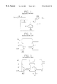
- FIG. 1 illustrates a conventional RC delay circuit.
- the conventional RC delay circuit includes an inverter IN 1 which inverts an input signal IN, a RC delay unit 10 which delays an output from the inverter IN 1 and a NOR gate NR 1 which NORs outputs from the inverter IN 1 and the RC delay unit 10 , the RC delay unit 10 consisting of a resistor R and an n-type MOS capacitor 12 .
- the output signal OUT has the same delay time in each cycle.
- a second cycle of the input signal IN may be inputted to the MOS capacitor 12 when a first cycle of the input signal IN is not fully charged in the capacitor 12 .
- the level of the output signal B of the RC delay unit 10 decreases and accordingly the delay time d 2 of the output signal OUT is reduced.
- the delay time d 2 of the second cycle becomes shorter than the delay time d 1 of the first cycle.
- the conventional RC delay circuit has a problem that the periodic input signal IN is applied, the RC delay time of each cycle may not be identical. Accordingly, the semiconductor memory device can not maintain the time margin of the signals due to the unstable RC delay operation.
- the present invention is directed to a RC delay time stabilizing circuit which obviates the problems and disadvantages due to the conventional art.
- a RC delay time stabilizing circuit which includes an inverter which inverts an input signal, a RC delay unit which is charged/discharged in accordance with an output from the inverter, a pull-up MOS transistor connected between a source voltage terminal and an output terminal of the RC delay unit and having a gate for receiving the input signal, and an output unit which generates an output signal having an identical delay time in accordance with output levels of the inverter and the RC delay unit.
- FIG. 1 is a diagram of a conventional RC delay circuit
- FIG. 2 is a signal wave-form diagram of each unit when a single-cycle input signal is inputted in FIG. 1;
- FIG. 3 is a signal wave-form diagram of each unit when a periodic input signal is inputted in FIG. 1;
- FIG. 4 is a diagram of a RC delay time stabilizing circuit according to the present invention.
- FIG. 5 is a signal wave-form diagram of each unit when a periodic input signal is inputted in FIG. 4 .
- the RC delay time stabilizing circuit of the present invention is provided with an inverter IN 1 inverting an input signal IN, a RC delay unit 10 delaying an output from the inverter IN 1 , a P-type MOS transistor 20 pulling up an output node B of the RC delay unit 10 in accordance with the input signal IN and an output unit 30 receiving outputs from the inverter IN 1 and the RC delay unit 10 and outputting an output signal OUT which uniformly has a RC delay time, the RC delay unit 10 consisting of a resistor R and an N-type MOS capacitor 12 and the MOS transistor 20 being connected between a source voltage Vcc node and an output node B of the RC delay unit 10 .
- the output unit 30 consists of MOS transistors PM 2 , PM 1 , NM 1 which are serially connected between a source voltage Vcc and a ground voltage Vss, and a MOS transistor NM 2 which is connected in parallel to drains of the MOS transistors PM 1 , NM 1 and an output terminal thereof. Further, gates of the MOS transistors PM 1 , NM 1 are connected with an output terminal of the inverter IN 1 , and gates of the MOS transistors PM 2 , NM 2 are respectively connected with an output terminal of the RC delay unit 10 .
- the MOS transistors PM 1 , PM 2 are a P-type, while the MOS transistors NM 1 , NM 2 are an N-type.
- the MOS capacitor 12 of the RC delay unit 10 when then periodic input signal IN is inputted to the MOS capacitor 12 through the inverter IN 1 and the resistor R, the MOS capacitor 12 of the RC delay unit 10 repeatedly performs charging and discharging in accordance with a level of the input signal IN, and the MOS transistor 20 pulls up the output terminal of the RC delay unit 10 in accordance with the input signal IN. Accordingly, the output unit 30 outputs the signal OUT having the same delay time in each cycle of the input signal IN in accordance with the signal A outputted from the inverter IN 1 and the output signal B from the RC delay unit 10 . More specifically, the operation of the circuit according to the embodiment of the present invention will be described as an example of first and second cycles of the input signal IN.
- the output node B of the RC delay unit 10 is pulled up by the turned-on MOS transistor 20 .
- the output node B is charged by the charging operation of the MOS capacitor 12 and the pull-up of the MOS transistor 20 , thereby decreasing the overall charging time.
- the delay time d 2 of the output signal OUT in the second cycle is the same as the delay time d 1 thereof in the first cycle since the output node B has been fully charged.
- the RC delay time stabilizing circuit of the present invention decreases the charging time of the RC delay unit when the periodic signal is inputted, thus maintaining the same delay time in each cycle of the input signal.
Landscapes
- Physics & Mathematics (AREA)
- Nonlinear Science (AREA)
- Pulse Circuits (AREA)
Abstract
Description
Claims (14)
Applications Claiming Priority (4)
| Application Number | Priority Date | Filing Date | Title |
|---|---|---|---|
| KR98-39308 | 1998-09-22 | ||
| KR19980039308 | 1998-09-22 | ||
| KR99-5030 | 1999-02-12 | ||
| KR1019990005030A KR20000022571A (en) | 1998-09-22 | 1999-02-12 | Rc delay time stabilization circuit |
Publications (1)
| Publication Number | Publication Date |
|---|---|
| US6320443B1 true US6320443B1 (en) | 2001-11-20 |
Family
ID=26634142
Family Applications (1)
| Application Number | Title | Priority Date | Filing Date |
|---|---|---|---|
| US09/377,165 Expired - Fee Related US6320443B1 (en) | 1998-09-22 | 1999-08-19 | RC delay time stabilizing circuit |
Country Status (2)
| Country | Link |
|---|---|
| US (1) | US6320443B1 (en) |
| KR (1) | KR20000022571A (en) |
Cited By (6)
| Publication number | Priority date | Publication date | Assignee | Title |
|---|---|---|---|---|
| US20040249991A1 (en) * | 2003-06-03 | 2004-12-09 | Dell Products L.P. | Cable detection using cable capacitance |
| US20070296479A1 (en) * | 2006-06-26 | 2007-12-27 | Nec Elecronics Corporation | Delay circuit |
| US9065324B2 (en) | 2013-10-23 | 2015-06-23 | Taiwan Semiconductor Manufacturing Company, Ltd. | Electronic device with PVT delay compensation and related method |
| US20200350915A1 (en) * | 2019-05-03 | 2020-11-05 | Taiwan Semiconductor Manufacturing Company Ltd. | Logic buffer circuit and method |
| US10998893B2 (en) | 2018-08-01 | 2021-05-04 | Micron Technology, Inc. | Semiconductor device, delay circuit, and related method |
| US11916548B2 (en) * | 2019-05-03 | 2024-02-27 | Taiwan Semiconductor Manufacturing Company, Ltd. | Logic buffer circuit and method |
Families Citing this family (1)
| Publication number | Priority date | Publication date | Assignee | Title |
|---|---|---|---|---|
| KR100897717B1 (en) * | 2002-07-19 | 2009-05-15 | 매그나칩 반도체 유한회사 | Automatic Calibration RC Delay Device |
Citations (8)
| Publication number | Priority date | Publication date | Assignee | Title |
|---|---|---|---|---|
| US4063117A (en) * | 1977-01-07 | 1977-12-13 | National Semiconductor Corporation | Circuit for increasing the output current in MOS transistors |
| US4617529A (en) * | 1984-08-23 | 1986-10-14 | Fujitsu Limited | Ring oscillator with delay element and potential pulling circuit |
| US5068553A (en) * | 1988-10-31 | 1991-11-26 | Texas Instruments Incorporated | Delay stage with reduced Vdd dependence |
| US5654981A (en) * | 1994-05-31 | 1997-08-05 | Texas Instruments Incorporated | Signal transmission system and method of operation |
| US5734284A (en) | 1996-10-11 | 1998-03-31 | Northern Telecom Limited | RC circuit |
| US5986463A (en) * | 1996-05-30 | 1999-11-16 | Nec Corporation | Differential signal generating circuit having current spike suppressing circuit |
| US6060930A (en) * | 1997-11-01 | 2000-05-09 | Lg Semicon Co., Ltd. | Delay circuit |
| US6097231A (en) * | 1998-05-29 | 2000-08-01 | Ramtron International Corporation | CMOS RC equivalent delay circuit |
-
1999
- 1999-02-12 KR KR1019990005030A patent/KR20000022571A/en not_active Ceased
- 1999-08-19 US US09/377,165 patent/US6320443B1/en not_active Expired - Fee Related
Patent Citations (8)
| Publication number | Priority date | Publication date | Assignee | Title |
|---|---|---|---|---|
| US4063117A (en) * | 1977-01-07 | 1977-12-13 | National Semiconductor Corporation | Circuit for increasing the output current in MOS transistors |
| US4617529A (en) * | 1984-08-23 | 1986-10-14 | Fujitsu Limited | Ring oscillator with delay element and potential pulling circuit |
| US5068553A (en) * | 1988-10-31 | 1991-11-26 | Texas Instruments Incorporated | Delay stage with reduced Vdd dependence |
| US5654981A (en) * | 1994-05-31 | 1997-08-05 | Texas Instruments Incorporated | Signal transmission system and method of operation |
| US5986463A (en) * | 1996-05-30 | 1999-11-16 | Nec Corporation | Differential signal generating circuit having current spike suppressing circuit |
| US5734284A (en) | 1996-10-11 | 1998-03-31 | Northern Telecom Limited | RC circuit |
| US6060930A (en) * | 1997-11-01 | 2000-05-09 | Lg Semicon Co., Ltd. | Delay circuit |
| US6097231A (en) * | 1998-05-29 | 2000-08-01 | Ramtron International Corporation | CMOS RC equivalent delay circuit |
Cited By (11)
| Publication number | Priority date | Publication date | Assignee | Title |
|---|---|---|---|---|
| US20040249991A1 (en) * | 2003-06-03 | 2004-12-09 | Dell Products L.P. | Cable detection using cable capacitance |
| US20070296479A1 (en) * | 2006-06-26 | 2007-12-27 | Nec Elecronics Corporation | Delay circuit |
| US7746141B2 (en) * | 2006-06-26 | 2010-06-29 | Nec Electronics Corporation | Delay circuit |
| US9065324B2 (en) | 2013-10-23 | 2015-06-23 | Taiwan Semiconductor Manufacturing Company, Ltd. | Electronic device with PVT delay compensation and related method |
| US10998893B2 (en) | 2018-08-01 | 2021-05-04 | Micron Technology, Inc. | Semiconductor device, delay circuit, and related method |
| US11342906B2 (en) * | 2018-08-01 | 2022-05-24 | Micron Technology, Inc. | Delay circuits, and related semiconductor devices and methods |
| US20200350915A1 (en) * | 2019-05-03 | 2020-11-05 | Taiwan Semiconductor Manufacturing Company Ltd. | Logic buffer circuit and method |
| US10979049B2 (en) * | 2019-05-03 | 2021-04-13 | Taiwan Semiconductor Manufacturing Company Ltd. | Logic buffer circuit and method |
| US20210234541A1 (en) * | 2019-05-03 | 2021-07-29 | Taiwan Semiconductor Manufacturing Company Ltd. | Logic buffer circuit and method |
| US11545977B2 (en) * | 2019-05-03 | 2023-01-03 | Taiwan Semiconductor Manufacturing Company, Ltd. | Logic buffer circuit and method |
| US11916548B2 (en) * | 2019-05-03 | 2024-02-27 | Taiwan Semiconductor Manufacturing Company, Ltd. | Logic buffer circuit and method |
Also Published As
| Publication number | Publication date |
|---|---|
| KR20000022571A (en) | 2000-04-25 |
Similar Documents
| Publication | Publication Date | Title |
|---|---|---|
| EP0254212B1 (en) | Mos semiconductor circuit | |
| US4757214A (en) | Pulse generator circuit | |
| KR100440448B1 (en) | Semiconductor integrated circuit device capable of securing time delay insensitive to temperature variation | |
| US4837466A (en) | Delay circuit | |
| US5097159A (en) | Delay circuit for delaying an output signal relative to an input signal for a specified time interval | |
| US5777497A (en) | CMOS output circuit with precharge circuit | |
| US4431927A (en) | MOS Capacitive bootstrapping trigger circuit for a clock generator | |
| US6320443B1 (en) | RC delay time stabilizing circuit | |
| JPH1022796A (en) | Timing circuit | |
| KR0163447B1 (en) | Data out buffer circuit | |
| US6346841B2 (en) | Pulse generator | |
| US4239991A (en) | Clock voltage generator for semiconductor memory | |
| US5495189A (en) | Non-overlap signal generation circuit | |
| US4392066A (en) | Schmidt trigger circuit | |
| JPH0123003B2 (en) | ||
| US5734282A (en) | Address transition detection circuit | |
| US6873192B2 (en) | Power-up detection apparatus | |
| EP0619652A2 (en) | Data output circuit | |
| KR20000018628A (en) | Output buffer for low noise having load adaptation type | |
| US5815464A (en) | Address transition detection circuit | |
| KR100189746B1 (en) | Signal output circuit for power on reset | |
| KR100313512B1 (en) | Power on detect circuit | |
| KR100245559B1 (en) | Data output buffer circuit | |
| KR0149578B1 (en) | Time delay circuit of semiconductor memory device | |
| JPH09261021A (en) | Signal transition detection circuit |
Legal Events
| Date | Code | Title | Description |
|---|---|---|---|
| AS | Assignment |
Owner name: HYUNDAI MICRO ELECTRONICS CO., LTD., KOREA, REPUBL Free format text: ASSIGNMENT OF ASSIGNORS INTEREST;ASSIGNOR:JEONG, YOUNG-HAN;REEL/FRAME:010191/0532 Effective date: 19990810 |
|
| AS | Assignment |
Owner name: HYUNDAI ELECTRONICS INDUSTRIES CO., LTD., KOREA, R Free format text: MERGER;ASSIGNOR:HYUNDAI MICRO ELECTRONICS CO. LTD.;REEL/FRAME:010985/0001 Effective date: 20000621 |
|
| FEPP | Fee payment procedure |
Free format text: PAYOR NUMBER ASSIGNED (ORIGINAL EVENT CODE: ASPN); ENTITY STATUS OF PATENT OWNER: LARGE ENTITY |
|
| FPAY | Fee payment |
Year of fee payment: 4 |
|
| FPAY | Fee payment |
Year of fee payment: 8 |
|
| FEPP | Fee payment procedure |
Free format text: PAYER NUMBER DE-ASSIGNED (ORIGINAL EVENT CODE: RMPN); ENTITY STATUS OF PATENT OWNER: LARGE ENTITY Free format text: PAYOR NUMBER ASSIGNED (ORIGINAL EVENT CODE: ASPN); ENTITY STATUS OF PATENT OWNER: LARGE ENTITY |
|
| REMI | Maintenance fee reminder mailed | ||
| LAPS | Lapse for failure to pay maintenance fees | ||
| STCH | Information on status: patent discontinuation |
Free format text: PATENT EXPIRED DUE TO NONPAYMENT OF MAINTENANCE FEES UNDER 37 CFR 1.362 |
|
| FP | Lapsed due to failure to pay maintenance fee |
Effective date: 20131120 |