US6313707B1 - Digital phase-locked loop with pulse controlled charge pump - Google Patents
Digital phase-locked loop with pulse controlled charge pump Download PDFInfo
- Publication number
- US6313707B1 US6313707B1 US09/188,194 US18819498A US6313707B1 US 6313707 B1 US6313707 B1 US 6313707B1 US 18819498 A US18819498 A US 18819498A US 6313707 B1 US6313707 B1 US 6313707B1
- Authority
- US
- United States
- Prior art keywords
- current
- capacitor
- controlled oscillator
- pulse
- magnitude
- Prior art date
- Legal status (The legal status is an assumption and is not a legal conclusion. Google has not performed a legal analysis and makes no representation as to the accuracy of the status listed.)
- Expired - Lifetime
Links
Images


Classifications
-
- H—ELECTRICITY
- H03—ELECTRONIC CIRCUITRY
- H03L—AUTOMATIC CONTROL, STARTING, SYNCHRONISATION, OR STABILISATION OF GENERATORS OF ELECTRONIC OSCILLATIONS OR PULSES
- H03L7/00—Automatic control of frequency or phase; Synchronisation
- H03L7/06—Automatic control of frequency or phase; Synchronisation using a reference signal applied to a frequency- or phase-locked loop
- H03L7/08—Details of the phase-locked loop
- H03L7/085—Details of the phase-locked loop concerning mainly the frequency- or phase-detection arrangement including the filtering or amplification of its output signal
- H03L7/089—Details of the phase-locked loop concerning mainly the frequency- or phase-detection arrangement including the filtering or amplification of its output signal the phase or frequency detector generating up-down pulses
- H03L7/0891—Details of the phase-locked loop concerning mainly the frequency- or phase-detection arrangement including the filtering or amplification of its output signal the phase or frequency detector generating up-down pulses the up-down pulses controlling source and sink current generators, e.g. a charge pump
- H03L7/0895—Details of the current generators
- H03L7/0898—Details of the current generators the source or sink current values being variable
-
- H—ELECTRICITY
- H03—ELECTRONIC CIRCUITRY
- H03L—AUTOMATIC CONTROL, STARTING, SYNCHRONISATION, OR STABILISATION OF GENERATORS OF ELECTRONIC OSCILLATIONS OR PULSES
- H03L7/00—Automatic control of frequency or phase; Synchronisation
- H03L7/06—Automatic control of frequency or phase; Synchronisation using a reference signal applied to a frequency- or phase-locked loop
- H03L7/08—Details of the phase-locked loop
- H03L7/10—Details of the phase-locked loop for assuring initial synchronisation or for broadening the capture range
- H03L7/107—Details of the phase-locked loop for assuring initial synchronisation or for broadening the capture range using a variable transfer function for the loop, e.g. low pass filter having a variable bandwidth
- H03L7/1072—Details of the phase-locked loop for assuring initial synchronisation or for broadening the capture range using a variable transfer function for the loop, e.g. low pass filter having a variable bandwidth by changing characteristics of the charge pump, e.g. changing the gain
-
- H—ELECTRICITY
- H03—ELECTRONIC CIRCUITRY
- H03L—AUTOMATIC CONTROL, STARTING, SYNCHRONISATION, OR STABILISATION OF GENERATORS OF ELECTRONIC OSCILLATIONS OR PULSES
- H03L7/00—Automatic control of frequency or phase; Synchronisation
- H03L7/06—Automatic control of frequency or phase; Synchronisation using a reference signal applied to a frequency- or phase-locked loop
- H03L7/08—Details of the phase-locked loop
- H03L7/085—Details of the phase-locked loop concerning mainly the frequency- or phase-detection arrangement including the filtering or amplification of its output signal
- H03L7/089—Details of the phase-locked loop concerning mainly the frequency- or phase-detection arrangement including the filtering or amplification of its output signal the phase or frequency detector generating up-down pulses
- H03L7/0891—Details of the phase-locked loop concerning mainly the frequency- or phase-detection arrangement including the filtering or amplification of its output signal the phase or frequency detector generating up-down pulses the up-down pulses controlling source and sink current generators, e.g. a charge pump
- H03L7/0895—Details of the current generators
- H03L7/0896—Details of the current generators the current generators being controlled by differential up-down pulses
-
- H—ELECTRICITY
- H03—ELECTRONIC CIRCUITRY
- H03L—AUTOMATIC CONTROL, STARTING, SYNCHRONISATION, OR STABILISATION OF GENERATORS OF ELECTRONIC OSCILLATIONS OR PULSES
- H03L7/00—Automatic control of frequency or phase; Synchronisation
- H03L7/06—Automatic control of frequency or phase; Synchronisation using a reference signal applied to a frequency- or phase-locked loop
- H03L7/16—Indirect frequency synthesis, i.e. generating a desired one of a number of predetermined frequencies using a frequency- or phase-locked loop
- H03L7/18—Indirect frequency synthesis, i.e. generating a desired one of a number of predetermined frequencies using a frequency- or phase-locked loop using a frequency divider or counter in the loop
Definitions
- This invention relates generally to the design of phase locked loops. More particularly, it relates to a digital phase locked loop having improved acquisition and jitter characteristics, and/or having a high-current, high-precision charge pump.
- a conventional digital phase locked loop (PLL) 100 as shown in FIG. 1 comprises two main components: a digital phase detector 102 and a controlled oscillator 104 .
- a digital phase detector 102 receives both a reference frequency signal f REF and a variable frequency signal f VAR .
- the reference frequency signal f REF is, e.g., an output of a highly accurate crystal oscillator.
- the variable frequency signal f VAR is typically the output frequency, or the output frequency divided by a frequency divider 106 to provide a slower rate clock signal, allowing the use of a slower rate crystal oscillator or other clock source as the reference frequency signal f REF .
- the digital phase detector 102 compares the phase of the reference frequency signal f REF with that of the variable frequency signal f VAR to determine whether or not the relative phase and frequency of the output signal f OUT of the PLL 100 is higher or lower than expected.
- the digital phase detector 102 activates a slow down signal DN to the controlled oscillator 104 to slow down the frequency and/or shift the phase of the output frequency signal f OUT of the PLL 100 . If, on the other hand, the output frequency and/or phase of the output frequency signal F OUT is too low, the digital phase detector 102 provides a speed up signal UP to the controlled oscillator 104 to speed up the frequency and/or shift the phase of the output frequency signal f OUT of the PLL 100 . Thus, the controlled oscillator 104 adjusts its output frequency signal f OUT in accordance with UP/DN controls provided by the digital phase detector 102 .
- a popular mechanism is the use of a charge pump and a loop filter to transform the UP/DN pulse controls from the digital phase detector 102 into a voltage charged on a capacitor, which then controls the frequency of a voltage controlled oscillator (VCO) in the controlled oscillator 104 .
- VCO voltage controlled oscillator
- instruction signals from the digital phase detector 102 to the digitally controlled oscillator 104 have only two basic modes, i.e., UP and DN (and a third mode of neither up or down, typically represented by the simultaneous activation of both the UP and DN signals).
- the width of the UP and DN control signal pulses to the controlled oscillator 104 are varied based on the phase difference between the reference frequency signal F REF and the variable frequency f VAR .
- resolution in the width of the UP and DN control signal pulses results in a given amount of jitter and requires a given amount of acquisition time to lock phases.
- the resolution of the pulse width of both the UP and DN control signals is minimized, but nevertheless has a finite, digitally derived width limited by the speed of the digital logic for activating and deactivating the UP and DN control signal pulses.
- the digital phase detector 102 when the PLL 100 is locked, the digital phase detector 102 will activate both the UP and DN signals each having a minimum pulse width. Then, if the output frequency signal f OUT as determined by a comparison of the variable frequency signal F VAR to the reference frequency signal f REF falls behind, the digital phase detector 102 will widen the activation pulse of the UP control signal to have an appropriately larger width than the DN control signal. On the other hand, if the output frequency signal F OUT becomes ahead in phase as determined by a comparison of the variable frequency signal F VAR to the reference frequency signal F REF , then the digital phase detector 102 will widen the activation pulse of the DN control signal to be wider than the activation pulse of the UP control signal, which may be at a minimum pulse width.
- jitter and/or acquisition time characteristics of a conventional digital phase locked loop are related to the resolution of the control signals from a phase detector to a digitally controlled oscillator.
- requirements for more stable clock signals derived from digital phase locked loops continue to tighten, there has become a need for more accurate control of a digital phase locked loop to provide improved jitter and/or acquisition time characteristics over conventional digital phase locked loop devices.
- a pulse controlled charge pump having programmable current output comprises a current generator to generate a current pulse having a programmable current level based on a magnitude control input to the pulse controlled charge pump.
- a capacitor is adapted to be charged by the current pulse to the current level.
- a method of controlling a voltage controlled oscillator in accordance with the principles of the present invention comprises charging a capacitor with a current having a programmably variable current magnitude. A voltage level of the charged capacitor is output to the voltage controlled oscillator.
- FIG. 1 shows a conventional digital phase locked loop having a digital phase detector.
- FIGS. 3A and 3B show a schematic diagram of a digital phase detector with adaptive magnitude control as shown in FIG. 2 .
- FIG. 4 is a plot showing simulation waveforms for explaining the operation of the digital phase detector shown in FIGS. 2, 3 A and 3 B.
- FIG. 5 is a block diagram of an embodiment of a digitally controlled oscillator in accordance with the principles of another aspect of the invention.
- FIG. 6 is a block diagram of an embodiment of a pulse controlled charge pump shown in FIG. 5 .
- FIG. 8 is a schematic diagram of an exemplary charge pump mirror shown in FIG. 6 .
- FIG. 9 is a schematic diagram of an exemplary charge pump output unit shown in FIG. 6 .
- FIG. 10 is a schematic diagram of an exemplary bias current generator shown in FIG. 6 .
- the present invention provides another dimension of oscillator control from a digital phase detector by utilizing consecutive phase-frequency comparison results.
- the number of times that the phase comparison provides the same result i.e., the number of consecutive UP control signal pulses from a digital phase detector or the number of consecutive DN control signal pulses from the digital phase detector
- a quantity signal e.g., a magnitude control signal MC
- MC is provided by a digital phase detector to a digitally controlled oscillator, in accordance with the principles of the present invention.
- This magnitude control signal MC adaptively adjusts a step size in the digitally controlled oscillator, e.g., by increasing a pulse current to a charge capacitor driving a voltage controlled oscillator, resulting in a shorter acquisition time and smaller jitter (two very important design parameters for PLLs) as compared to conventional digital PLLs.
- FIG. 2 shows a block diagram of a digital PLL 200 having, in addition to otherwise conventional UP and DN control signals, a magnitude or step size control signal MC provided by a digital phase detector 202 to a digitally controlled oscillator 204 .
- a frequency divider 106 is optionally provided in a feedback path between an output frequency signal F OUT and a variable frequency signal f VAR input to a digital phase detector 202 , and a reference frequency signal F REF is input to the digital phase detector 202 , otherwise as in a conventional digital PLL, e.g., as shown in FIG. 1 .
- the digital phase detector 202 provides UP and DN control signals to a digitally controlled oscillator 204 .
- a digital phase detector 202 in addition to UP and DN control signals, a digital phase detector 202 in accordance with the principles of the present invention further provides a step size or magnitude control signal to the digitally controlled oscillator 204 to set an adjustment step size in the up and down directions for each UP and DN control signal.
- the adjusted size of the phase/frequency for each relative portion of the pulse width of both the UP and DN signals is set according to a desired parameter.
- the output frequency signal f OUT will likely be quite far from the frequency and/or phase of the reference frequency signal F REF .
- a large step size for each pulse width of the UP and/or DN control signals would be desired in the digitally controlled oscillator 204 to take larger and quicker strides toward outputting the ultimate frequency and/or phase from the PLL 200 .
- the digital phase detector 202 senses that the frequency and/or phase is approaching that of the desired frequency and/or phase of the reference frequency signal F REF , the step size of the adjustments in the digitally controlled oscillator 204 can be appropriately reduced for greater accuracy and lower jitter.
- the step size in the digitally controlled oscillator 204 can be set to a minimum by the digital phase detector 202 using the magnitude control signal MC to provide for the lowest jitter possible.
- larger step sizes in the adjustments of the digitally controlled oscillator 204 can be used initially to achieve faster acquisition of the target frequency and/or phase, while smaller step sizes can be subsequently used to provide a lowest possible jitter in the locked output frequency signal f OUT .
- the magnitude control signal may be a serial signal or a parallel signal, and may have virtually any number of values.
- the magnitude control signal may be a single bit line having only two settings, i.e., high for large step size and low for small step size.
- the magnitude control signal may be a multiple bit value passed over either a serial or parallel communication path to the digitally controlled oscillator 204 to provide multiple step size control of the adjustments to the output frequency signal f OUT .
- FIGS. 3A and 3B are a schematic diagram of an exemplary embodiment of the digital phase detector 202 shown in FIG. 2 .
- FIG. 3A shows the generation of the UP and DN control signals as well as other internally used control signals within the digital phase detector 202
- FIG. 3B shows the generation of a magnitude control signal MC, in accordance with the principles of the present invention.
- This embodiment of a digital phase detector 202 takes advantage of the small overlap time of the pulses of the UP/DN control signals to avoid short pulse effects as in a conventional digital phase detector, e.g., as shown in FIG. 1 .
- a buffer 306 provides a buffered clock signal RCK as well as an inverted clock signal /RCK, both based on the input reference frequency signal F REF .
- These buffered clock signals RCK and /RCK are used to clock a series of D type Flip-Flops 321 - 328 shown in FIG. 3 B.
- a three-bit magnitude control signal MC is generated mainly by two rows of D type Flip-Flops 321 - 328 .
- Flip-Flops 321 - 328 are positive edge triggered with synchronous clear when the RB input is at a logic LOW.
- the upper row of D type Flip-Flops 321 - 324 records the number of consecutive UP pulses
- the bottom row of D type Flip-Flops 325 - 328 records the number of consecutive DN pulses.
- the first D type Flip-Flop 321 in the first row inputs the UP control signal and is clocked by the DN and inverted DN signal (i.e., /DN control signal). It is preferable that the width of both the UP and DN control signals be minimized, e.g., to no greater than 0.5 nanoseconds (nS), to correct for the delays caused by the D type Flip-Flops 321 - 328 .
- nS nanoseconds
- f VAR leads f REF
- the UP waveform is a series of minimum width pulses and the DN pulse width is proportional to the amount of time that f VAR leads f REF .
- the width of the DN pulse has been reduced to its minimum and the UP pulse progressively widens as the lag between f VAR and f REF increases.
- the first D type Flip-Flop 325 in the second row inputs the DN control signal and is clocked by the UP and inverted UP signal (i.e., /UP control signal). Moreover, as shown by waveform (g) of FIG. 4, the output signal DX is maintained at a logic HIGH for the period that the phase of the variable frequency signal f VAR precedes that of the reference frequency signal f REF .
- the remaining D type Flip-Flops 322 - 324 and 326 - 328 shown in FIG. 3B are all clocked by the buffered clock signal RCK and the buffered and inverted clock signal /RCK, to form respective shift register chains.
- the length of the shift register chain (e.g., which is 3 as shown in FIG. 3B) can of course be varied according to design needs within the principles of the present invention.
- D type Flip-Flops 321 - 324 form an upper 3 bit shift register.
- UX is maintained at a logic HIGH as shown in waveform (f) of FIG. 4 for a range of 45 to 75 nS.
- the shift resistor signals U 1 to U 3 sequentially follow the UX signal to become respective logic HIGH levels on the rising edge of the reference frequency signal f REF .
- the signal UX becomes a logic LOW
- DX is high
- the logic at the bottom of FIG. 3A clears U 1 to U 3 to a logic LOW, and thus all bits of the upper shift register 322 to 324 are cleared.
- the D type Flip-Flops 326 - 328 form a lower 3 bit shift register.
- the signal DX shown in waveform (g) of FIG. 4 is maintained at a logic HIGH level in a range of 0 to 30 nS. This causes the shift register signals D 1 to D 3 to be sequentially clocked to logic HIGH levels on the rising edge of the reference frequency signal F REF .
- the signal DX becomes a logic LOW level
- UX becomes a logic HIGH
- the logic at the bottom of FIG. 3A clears D 1 to D 3 , and thus all bits of the lower shift register 326 - 328 are cleared.
- variable frequency signal F VAR When the variable frequency signal F VAR is aligned with the reference frequency signal F REF , the UP and DN control signals are both at minimum pulse width, the signals UX and DX both become a logic LOW level, and all of the D type Flip-Flops 321 - 328 in both the upper and lower rows are cleared, as shown in the range 35-40 nS in the waveforms of FIG. 4 .
- the U 1 to U 3 and D 1 to D 3 signals are synchronized by the rising edge of the reference frequency signal F REF and thus are late by a half cycle.
- U 1 to U 3 and D 1 to D 3 signals are logically ORed in bit-wise fashion by NOR gate(s) 312 , and inverted by an inverter if desired, to form a magnitude control signal MC in accordance with the principles of the present invention.
- D type Flip-Flops 322 - 324 and 326 - 328 are shown as forming a shift register, other configurations are within the scope of the present invention. For instance, instead of shift registers measuring the magnitude of the UP or DN control, a bit counter may be implemented in certain applications and appropriately interpreted within the controlled oscillator 104 to adjust a step size.
- a digital phase locked loop includes a digital phase detector which provides a magnitude control signal to adjust the step size of up and down adjustments of the phase/frequency of a digitally controlled oscillator, resulting in a shorter lock-in or acquisition time and a smaller jitter as compared to conventional digital phase locked loop devices.
- a charge pump in the digitally controlled oscillator 104 transforms the UP and DN pulse signals output by the digital phase frequency detector 102 into a pulse current for charging and discharging a capacitor in a related loop filter in the digitally controlled oscillator 104 .
- the pulsed current to the capacitor changes the voltage across the capacitor, which then controls the oscillating frequency of a voltage controlled oscillator (VCO).
- VCO voltage controlled oscillator
- FIGS. 5-10 relate to an embodiment of a pulse controlled charge pump 502 having magnitude control of a current pulse output.
- CMOS designs of charge pumps have some difficulty in providing a high current output with precision.
- the output current usually deviates from the targeted design value by a large percentage particularly because of short-channel effects.
- tight PLL specifications and noise performance requirements demand higher output currents, e.g., in a range of 175 to 2000 microamperes (uA), with high precision and low charge injection.
- Conventional charge pumps do not provide such high output current with the high precision necessary for many of today's applications, particularly when swung through a range of magnitude in accordance with the principles of the present invention.
- FIG. 5 is a block diagram of an embodiment of a digitally controlled oscillator 204 including a pulse controlled charge pump 502 having the unique combination of high-current and high-precision, and programmable magnitude input, in accordance with the principles of another aspect of the invention.
- the disclosed pulse controlled charge pump 502 was implemented using a 0.3 micrometer (um) CMOS process.
- the principles relate equally to any suitable manufacturing processes.
- the pulse controlled charge pump 502 receives the UP and DN signals as well as the magnitude control signal MC from the digital phase frequency detector 202 , and provides a high current, high precision output current pulse CPOUT having programmable range to a voltage controlled oscillator VCO 504 , which outputs the desired output frequency from the PLL 200 .
- VCO 504 voltage controlled oscillator
- the charge pump output CPOUT is a high precision programmable current from 175 uA to 2000 uA, with each subsequent current value being increased by a ratio of about the square root of two.
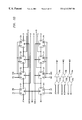
- FIG. 6 is a more detailed block diagram of an embodiment of a pulse controlled charge pump 502 shown in FIG. 5 .
- the pulse controlled charge pump 502 includes a pump current generator and multiplication control 602 , a charge pump current mirror 606 , and a charge pump output unit 608 .
- a bias current generator 604 provides bias current to the charge pump output unit to maintain a base or reference charge on the capacitor to maintain a reference frequency output from the PLL.
- the input signals to the pulse controlled charge pump 502 include the instruction signals UP and DN and their complements, UPB and DNB, respectively, a universal enable signal EN, a reference current input IBIAS (10 uA), and a three bit current magnitude control signal MC[ 2 : 0 ].
- Two bias current input signals IBN and IBP are input to the bias current generator 604 , which replicates the bias currents for each current driver.
- the bias current signals IBN[ 0 : 7 ] and IBP[ 0 : 7 ] output from the bias current generator are provided to the respective current mirrors within each current driver in the charge pump output unit 608 .
- the output from the pulse controlled charge pump 502 is the programmable, magnitude controllable output current pulse CPOUT.
- FIG. 7 is a schematic diagram of an exemplary pump current generator and multiplication control module shown in FIG. 6 .
- the magnitude control signal MC is provided to the first stage, i.e., to the pump current generator and multiplication control 602 .
- the least significant bit (LSB) of the magnitude control signal MC directly controls a current mirror to select a current output level, e.g., 17.5 or 25 uA in the disclosed embodiment.
- the most significant bits determine the number of unit drivers which will be enabled to provide the desired current magnitude.
- the pump current generator and multiplication control 602 receives the reference current IBIAS and the magnitude control signal MC, and outputs a current signal IPO and a plurality of multiplication controls signals X 2 , X 4 , X 8 .
- the current signal IPO is either 17.5 uA or 25 uA in the disclosed example, depending on the status of the LSB of the magnitude control signal. Thus, if the LSB is at a logic low, the current signal will be 17.5 uA, while if it is at a logic high, the current signal will be 25 uA in the disclosed example.
- the multiplication control signals X 2 , X 4 and X 8 are decoded from the most significant bits (MSBs) of the magnitude control signal MC, e.g., MC[ 2 : 1 ].
- MSBs most significant bits
- the multiplication control signal X 2 is enabled, two of the eight available current drivers in charge pump 608 will be enabled. (Additional details regarding the charge pump 608 will be discussed herein below following the discussion of the pump current generator and multiplication control 602 and the charge pump bias 606 .)
- the multiplication control signal X 4 is enabled, four of the current drivers will be enabled, and when the multiplication control signal X 8 is enabled, all eight current drivers will be enabled.
- the LSB of “-0” will select 17.5 uA for output by the current signal IPO. This is scaled by the bias generator 606 and the charge pump 608 to output 175 uA from CPOUT of 608 for each driver in 608 enabled by the magnitude control signal MC.
- the present embodiment implements up to eight current drivers, the use of fewer or more current drivers is within the scope of the present invention.
- FIG. 8 is a schematic diagram of an exemplary second stage, the charge pump current mirror bias generator 606 shown in FIG. 6 .
- the charge pump current mirror bias generator 606 comprises the devices that bias the wide-swing cascoded current mirror used in the charge pump 608 .
- the output signals N 10 -N 13 provide suitable bias voltages for the current drivers in the charge pump output unit 608 .
- the bias circuit 606 links the internal current signal IPO to the multiple output drivers in the charge pump output unit 608 , which can each be used in either direction, i.e., as a current source or as a current sink.
- FIG. 9 is a schematic diagram of one driver of an exemplary charge pump output unit shown in FIG. 6 .
- the final stage of the pulse controlled charge pump 502 , the charge pump output unit 608 is an array of, e.g., eight unit current drivers, each outputting a current of 175 uA or 250 uA, depending upon the status of the magnitude control signal.
- FIG. 9 shows one such driver 608 a.
- Each driver 608 a is provided with a unique, individual enable signal to allow programmability in the output current with a resolution as small as one driver. Obviously, the more drivers that are enabled, the higher the total output current.
- the input to each driver 608 a includes the universal enable signal EN, a block enable signal ENBLK, the instruction signals UP and DN and their complement signals UPB and DNB, respectively.
- the output ports CPOUT( 1 ) of each of the eight drivers 608 a are tied together to provide the total current for a pulse output signal CPOUT to the VCO 504 (FIG. 5 ).
- the exemplary driver shown in FIG. 9 comprises two cascoded MOS transistors 910 and 912 connected to a power source VDDA and providing a current source, while cascoded MOS transistors 914 and 916 connected to ground VSSA provide a current sink.
- Two switch controlled paths IA and IB are connected to the output path CPOUT( 1 ), while two balancing paths IC and ID are connected to a pull-down amplifier 902 and pull-up amplifier 904 , respectively. Both the pull-down amplifier 902 and the pull-up amplifier 904 are enabled by the combined enable signals ENX and ENBX.
- the balancing paths IC and ID together with the pull-down amplifier 902 and pull-up amplifier 904 provide protection from the effects of charge injection.
- the cascoded transistors 914 and 916 sink current input from the current output line CPOUT( 1 ) when the path IA is switched off. Similarly, the cascoded transistors 910 and 912 feed a current to the current output line CPOUT( 1 ) when the path IB is switched off. Operation of the cascoded transistor current source 910 and 912 as well as the cascoded transistor current sink 914 and 916 are enabled by the combined enable signals ENX and ENBX.
- the amount of current sourced by each driver 608 a is set by the signals N 12 and N 13 , and the amount of current sunk by each driver 608 a is set by the signals N 10 and N 11 .
- the four switches 940 - 946 are controlled by the up and down instruction pulses UPX and DNX together with their complementary signals UPBX and DNBX, respectively (the ‘X’ representing the driver number).
- the switch 942 is used to connect the cascode current source 912 and 910 to the output when the charge pump is to source current. When the driver is to sink current, switch 942 is open and switch 944 closes so the cascode current source 914 and 916 can pull current from the output. To minimize the effects of switching the current source on and off, the cascode current source 912 is connected to node ID through switch 940 when switch 942 is open.
- the pull-down amplifier 902 tracks the output node voltage (CPOUT( 1 )) so the drain of the cascode current source 912 is operating at the same potential as if switch 942 was closed.
- switch 946 and pull-up amplifier 904 are used to keep the cascode current source 914 at the same potential as CPOUT when switch 944 is open. This method of minimizing the current switching transients is discussed in detail in U.S. application Ser. No. 09/188,241, by Wenzhe Luo, entitled “Reduced Charge Injection In Current Switch”, co-filed on even date herewith.
- the pulse controlled charge pump 502 as shown in FIG. 9 has greatly minimized MOS charge injection effects.
- FIG. 10 is a schematic diagram of an exemplary bias current generator 604 shown in FIG. 6 .
- the bias current generator replicates the current input signals IBP and IBN for use by each current driver 608 a in the charge pump output unit 608 .
- the bias current signals IBN[ 0 : 7 ] and IBP[ 0 : 7 ] output from the bias current generator 604 are provided to the respective pull-up amplifiers 904 and pull-down amplifiers 902 , respectively, within each current driver 608 a in the charge pump output unit 608 .
- the invention has particular application for cordless devices, and/or particularly in the design of phase-locked loops which utilize a digital phase-detector and a charge pump.
- pulse controlled charge pump relates to an adjustable current output of 175 or 250 microamperes (uA), the principles relate particularly to adjustments among any output level.
Abstract
Description
Claims (12)
Priority Applications (1)
| Application Number | Priority Date | Filing Date | Title |
|---|---|---|---|
| US09/188,194 US6313707B1 (en) | 1998-11-09 | 1998-11-09 | Digital phase-locked loop with pulse controlled charge pump |
Applications Claiming Priority (1)
| Application Number | Priority Date | Filing Date | Title |
|---|---|---|---|
| US09/188,194 US6313707B1 (en) | 1998-11-09 | 1998-11-09 | Digital phase-locked loop with pulse controlled charge pump |
Publications (1)
| Publication Number | Publication Date |
|---|---|
| US6313707B1 true US6313707B1 (en) | 2001-11-06 |
Family
ID=22692128
Family Applications (1)
| Application Number | Title | Priority Date | Filing Date |
|---|---|---|---|
| US09/188,194 Expired - Lifetime US6313707B1 (en) | 1998-11-09 | 1998-11-09 | Digital phase-locked loop with pulse controlled charge pump |
Country Status (1)
| Country | Link |
|---|---|
| US (1) | US6313707B1 (en) |
Cited By (16)
| Publication number | Priority date | Publication date | Assignee | Title |
|---|---|---|---|---|
| US20030137290A1 (en) * | 2000-12-19 | 2003-07-24 | Lu Shih-Lien L. | Phase detector |
| US6710665B2 (en) | 2001-01-26 | 2004-03-23 | True Circuits, Inc. | Phase-locked loop with conditioned charge pump output |
| US6747520B1 (en) | 2002-07-12 | 2004-06-08 | Marvell International Ltd. | Limit swing charge pump and method thereof |
| US20040135640A1 (en) * | 2002-01-28 | 2004-07-15 | Maneatis John G. | Phase-locked loop with conditioned charge pump output |
| US6774732B1 (en) * | 2003-02-14 | 2004-08-10 | Motorola, Inc. | System and method for coarse tuning a phase locked loop (PLL) synthesizer using 2-PI slip detection |
| US6871051B1 (en) * | 2000-06-26 | 2005-03-22 | Keith Barr | Serial data transmission system using minimal interface |
| US7064600B1 (en) | 2002-07-12 | 2006-06-20 | Marvell International Ltd. | Limit swing charge pump and method thereof |
| US20070018701A1 (en) * | 2005-07-20 | 2007-01-25 | M/A-Com, Inc. | Charge pump apparatus, system, and method |
| US20070090884A1 (en) * | 2005-10-26 | 2007-04-26 | Microchip Technology Incorporated | Method, System and Apparatus for Reducing Oscillator Frequency Spiking During Oscillator Frequency Adjustment |
| US7315197B1 (en) | 2002-07-12 | 2008-01-01 | Marvell International Ltd. | Limit swing charge pump and method thereof |
| WO2008074129A1 (en) * | 2006-12-21 | 2008-06-26 | Icera Canada ULC | Digital charge pump pll architecture |
| US20080191760A1 (en) * | 2007-02-12 | 2008-08-14 | Analogix Semiconductor, Inc. | PLLS covering wide operating frequency ranges |
| US20100327931A1 (en) * | 2009-06-29 | 2010-12-30 | Saad Mohammad Al-Shahrani | Wideband programmable phase shifting circuit |
| US8638144B1 (en) | 2009-12-30 | 2014-01-28 | Gsi Technology, Inc. | Systems and methods involving phase detection with adaptive locking/detection features |
| US9356611B1 (en) | 2009-12-30 | 2016-05-31 | Gsi Technology, Inc. | Systems and methods involving phase detection with adaptive locking/detection features |
| WO2022247843A1 (en) * | 2021-05-27 | 2022-12-01 | 广东工业大学 | Low-power-consumption negative pressure generator for radio frequency switch |
Citations (4)
| Publication number | Priority date | Publication date | Assignee | Title |
|---|---|---|---|---|
| US5313499A (en) * | 1992-04-29 | 1994-05-17 | International Business Machines Corporation | Constant gain phase lock-loop |
| US5625325A (en) * | 1995-12-22 | 1997-04-29 | Microtune, Inc. | System and method for phase lock loop gain stabilization |
| US5783972A (en) * | 1995-11-29 | 1998-07-21 | Nec Corporation | Power saving PLL circuit |
| US5831483A (en) * | 1996-01-30 | 1998-11-03 | Nec Corporation | PLL frequency synthesizer having circuit for controlling gain of charge pump circuit |
-
1998
- 1998-11-09 US US09/188,194 patent/US6313707B1/en not_active Expired - Lifetime
Patent Citations (4)
| Publication number | Priority date | Publication date | Assignee | Title |
|---|---|---|---|---|
| US5313499A (en) * | 1992-04-29 | 1994-05-17 | International Business Machines Corporation | Constant gain phase lock-loop |
| US5783972A (en) * | 1995-11-29 | 1998-07-21 | Nec Corporation | Power saving PLL circuit |
| US5625325A (en) * | 1995-12-22 | 1997-04-29 | Microtune, Inc. | System and method for phase lock loop gain stabilization |
| US5831483A (en) * | 1996-01-30 | 1998-11-03 | Nec Corporation | PLL frequency synthesizer having circuit for controlling gain of charge pump circuit |
Cited By (30)
| Publication number | Priority date | Publication date | Assignee | Title |
|---|---|---|---|---|
| US6871051B1 (en) * | 2000-06-26 | 2005-03-22 | Keith Barr | Serial data transmission system using minimal interface |
| US20030137290A1 (en) * | 2000-12-19 | 2003-07-24 | Lu Shih-Lien L. | Phase detector |
| US6803753B2 (en) * | 2000-12-19 | 2004-10-12 | Intel Corporation | Frequency phase detector for differentiating frequencies having small phase differences |
| US6710665B2 (en) | 2001-01-26 | 2004-03-23 | True Circuits, Inc. | Phase-locked loop with conditioned charge pump output |
| US7292106B2 (en) | 2002-01-28 | 2007-11-06 | True Circuits, Inc. | Phase-locked loop with conditioned charge pump output |
| US20040135640A1 (en) * | 2002-01-28 | 2004-07-15 | Maneatis John G. | Phase-locked loop with conditioned charge pump output |
| US20060012441A1 (en) * | 2002-01-28 | 2006-01-19 | True Circuits, Inc. | Phase-locked loop with conditioned charge pump output |
| US6819187B1 (en) | 2002-07-12 | 2004-11-16 | Marvell International Ltd. | Limit swing charge pump and method thereof |
| US7064600B1 (en) | 2002-07-12 | 2006-06-20 | Marvell International Ltd. | Limit swing charge pump and method thereof |
| US6747520B1 (en) | 2002-07-12 | 2004-06-08 | Marvell International Ltd. | Limit swing charge pump and method thereof |
| US7315197B1 (en) | 2002-07-12 | 2008-01-01 | Marvell International Ltd. | Limit swing charge pump and method thereof |
| WO2004075411A3 (en) * | 2003-02-14 | 2004-12-23 | Freescale Semiconductor Inc | System and method for coarse tuning a phase locked loop (pll) synthesizer using 2-pi slip detection |
| WO2004075411A2 (en) * | 2003-02-14 | 2004-09-02 | Freescale Semiconductor, Inc. | System and method for coarse tuning a phase locked loop (pll) synthesizer using 2-pi slip detection |
| US6774732B1 (en) * | 2003-02-14 | 2004-08-10 | Motorola, Inc. | System and method for coarse tuning a phase locked loop (PLL) synthesizer using 2-PI slip detection |
| KR101082724B1 (en) * | 2003-02-14 | 2011-11-10 | 프리스케일 세미컨덕터, 인크. | 2 system and method for coarse tuning a phase locked looppll synthesizer using 2-pi slip detection |
| US20070018701A1 (en) * | 2005-07-20 | 2007-01-25 | M/A-Com, Inc. | Charge pump apparatus, system, and method |
| US7432773B2 (en) * | 2005-10-26 | 2008-10-07 | Microchip Technology Incorporated | Method, system and apparatus for reducing oscillator frequency spiking during oscillator frequency adjustment |
| US20070090884A1 (en) * | 2005-10-26 | 2007-04-26 | Microchip Technology Incorporated | Method, System and Apparatus for Reducing Oscillator Frequency Spiking During Oscillator Frequency Adjustment |
| US8004326B2 (en) | 2006-12-21 | 2011-08-23 | Icera Canada ULC | Digital charge pump PLL architecture |
| WO2008074129A1 (en) * | 2006-12-21 | 2008-06-26 | Icera Canada ULC | Digital charge pump pll architecture |
| US20100060333A1 (en) * | 2006-12-21 | 2010-03-11 | Icera Canada ULC | Digital charge pump pll architecture |
| US7692497B2 (en) | 2007-02-12 | 2010-04-06 | Analogix Semiconductor, Inc. | PLLS covering wide operating frequency ranges |
| US20080191760A1 (en) * | 2007-02-12 | 2008-08-14 | Analogix Semiconductor, Inc. | PLLS covering wide operating frequency ranges |
| US7893745B2 (en) | 2009-06-29 | 2011-02-22 | King Fahd University Of Petroleum And Minerals | Wideband programmable phase shifting circuit |
| US20100327931A1 (en) * | 2009-06-29 | 2010-12-30 | Saad Mohammad Al-Shahrani | Wideband programmable phase shifting circuit |
| US8638144B1 (en) | 2009-12-30 | 2014-01-28 | Gsi Technology, Inc. | Systems and methods involving phase detection with adaptive locking/detection features |
| US9018992B1 (en) | 2009-12-30 | 2015-04-28 | Gsi Technology, Inc. | Systems and methods involving phase detection with adaptive locking/detection features |
| US9356611B1 (en) | 2009-12-30 | 2016-05-31 | Gsi Technology, Inc. | Systems and methods involving phase detection with adaptive locking/detection features |
| WO2022247843A1 (en) * | 2021-05-27 | 2022-12-01 | 广东工业大学 | Low-power-consumption negative pressure generator for radio frequency switch |
| US11711075B2 (en) | 2021-05-27 | 2023-07-25 | Guangdong University Of Technology | Low-power consumption negative voltage generator for radio frequency switches |
Similar Documents
| Publication | Publication Date | Title |
|---|---|---|
| US6313707B1 (en) | Digital phase-locked loop with pulse controlled charge pump | |
| US6628154B2 (en) | Digitally controlled analog delay locked loop (DLL) | |
| US7746181B1 (en) | Circuit and method for extending the usable frequency range of a phase locked loop (PLL) | |
| US7327176B2 (en) | Delay circuit and delay synchronization loop device | |
| US7193907B2 (en) | Semiconductor integrated circuit having a power-on reset circuit in a semiconductor memory device | |
| JP4337108B2 (en) | Analog mixed digital DLL | |
| US8207769B2 (en) | Delay locked loop circuit | |
| US6147561A (en) | Phase/frequency detector with time-delayed inputs in a charge pump based phase locked loop and a method for enhancing the phase locked loop gain | |
| EP1933464B1 (en) | Adaptive bandwith phase locked loop with feedforward divider | |
| KR100429127B1 (en) | Synchronous device | |
| US7282971B2 (en) | Digital delay lock loop | |
| US7719331B2 (en) | PLL circuit | |
| US6674824B1 (en) | Method and circuitry for controlling a phase-locked loop by analog and digital signals | |
| US20030222694A1 (en) | Method and/or circuit for generating precision programmable multiple phase angle clocks | |
| JP5719333B2 (en) | Phase shift processing in delay locked loop / phase locked loop | |
| JP3331115B2 (en) | Frequency phase locked loop | |
| US7551012B2 (en) | Phase shifting in DLL/PLL | |
| US6140852A (en) | Digital phase-locked loop with pulse controlled charge pump | |
| US7113014B1 (en) | Pulse width modulator | |
| EP0986178A2 (en) | Frequency synthesizer | |
| US6222401B1 (en) | Phase locked loop using gear shifting algorithm | |
| JP3854065B2 (en) | Phase compensation clock synchronization circuit | |
| JP2000091896A (en) | Delay adjusting device | |
| KR20010064098A (en) | Digital Delay Locked Loop with analog delay | |
| US20220158628A1 (en) | Clock signal generation |
Legal Events
| Date | Code | Title | Description |
|---|---|---|---|
| AS | Assignment |
Owner name: LUCENT TECHNOLGIES INC., NEW JERSEY Free format text: ASSIGNMENT OF ASSIGNORS INTEREST;ASSIGNORS:FISCHER, JONATHAN H.;LUO, WENZHE;MA, ZHIGANG;REEL/FRAME:009590/0912 Effective date: 19981109 |
|
| STCF | Information on status: patent grant |
Free format text: PATENTED CASE |
|
| AS | Assignment |
Owner name: AGERE SYSTEMS INC., PENNSYLVANIA Free format text: ASSIGNMENT OF ASSIGNORS INTEREST;ASSIGNOR:LUCENT TECHNOLOGIES INC.;REEL/FRAME:015991/0893 Effective date: 20010130 |
|
| FPAY | Fee payment |
Year of fee payment: 4 |
|
| FPAY | Fee payment |
Year of fee payment: 8 |
|
| FPAY | Fee payment |
Year of fee payment: 12 |
|
| AS | Assignment |
Owner name: DEUTSCHE BANK AG NEW YORK BRANCH, AS COLLATERAL AG Free format text: PATENT SECURITY AGREEMENT;ASSIGNORS:LSI CORPORATION;AGERE SYSTEMS LLC;REEL/FRAME:032856/0031 Effective date: 20140506 |
|
| AS | Assignment |
Owner name: AVAGO TECHNOLOGIES GENERAL IP (SINGAPORE) PTE. LTD Free format text: ASSIGNMENT OF ASSIGNORS INTEREST;ASSIGNOR:AGERE SYSTEMS LLC;REEL/FRAME:035365/0634 Effective date: 20140804 |
|
| AS | Assignment |
Owner name: LSI CORPORATION, CALIFORNIA Free format text: TERMINATION AND RELEASE OF SECURITY INTEREST IN PATENT RIGHTS (RELEASES RF 032856-0031);ASSIGNOR:DEUTSCHE BANK AG NEW YORK BRANCH, AS COLLATERAL AGENT;REEL/FRAME:037684/0039 Effective date: 20160201 Owner name: AGERE SYSTEMS LLC, PENNSYLVANIA Free format text: TERMINATION AND RELEASE OF SECURITY INTEREST IN PATENT RIGHTS (RELEASES RF 032856-0031);ASSIGNOR:DEUTSCHE BANK AG NEW YORK BRANCH, AS COLLATERAL AGENT;REEL/FRAME:037684/0039 Effective date: 20160201 |
|
| AS | Assignment |
Owner name: BANK OF AMERICA, N.A., AS COLLATERAL AGENT, NORTH CAROLINA Free format text: PATENT SECURITY AGREEMENT;ASSIGNOR:AVAGO TECHNOLOGIES GENERAL IP (SINGAPORE) PTE. LTD.;REEL/FRAME:037808/0001 Effective date: 20160201 Owner name: BANK OF AMERICA, N.A., AS COLLATERAL AGENT, NORTH Free format text: PATENT SECURITY AGREEMENT;ASSIGNOR:AVAGO TECHNOLOGIES GENERAL IP (SINGAPORE) PTE. LTD.;REEL/FRAME:037808/0001 Effective date: 20160201 |
|
| AS | Assignment |
Owner name: AVAGO TECHNOLOGIES GENERAL IP (SINGAPORE) PTE. LTD., SINGAPORE Free format text: TERMINATION AND RELEASE OF SECURITY INTEREST IN PATENTS;ASSIGNOR:BANK OF AMERICA, N.A., AS COLLATERAL AGENT;REEL/FRAME:041710/0001 Effective date: 20170119 Owner name: AVAGO TECHNOLOGIES GENERAL IP (SINGAPORE) PTE. LTD Free format text: TERMINATION AND RELEASE OF SECURITY INTEREST IN PATENTS;ASSIGNOR:BANK OF AMERICA, N.A., AS COLLATERAL AGENT;REEL/FRAME:041710/0001 Effective date: 20170119 |
|
| AS | Assignment |
Owner name: AVAGO TECHNOLOGIES INTERNATIONAL SALES PTE. LIMITE Free format text: ASSIGNMENT OF ASSIGNORS INTEREST;ASSIGNOR:AVAGO TECHNOLOGIES GENERAL IP (SINGAPORE) PTE. LTD.;REEL/FRAME:047022/0620 Effective date: 20180509 |
|
| AS | Assignment |
Owner name: AVAGO TECHNOLOGIES INTERNATIONAL SALES PTE. LIMITE Free format text: CORRECTIVE ASSIGNMENT TO CORRECT THE NATURE OF CONVEYANCE AND EFFECTIVE DATE PREVIOUSLY RECORDED ON REEL 047022 FRAME 0620. ASSIGNOR(S) HEREBY CONFIRMS THE MERGER;ASSIGNOR:AVAGO TECHNOLOGIES GENERAL IP (SINGAPORE) PTE. LTD.;REEL/FRAME:047185/0643 Effective date: 20180509 |
|
| AS | Assignment |
Owner name: AVAGO TECHNOLOGIES INTERNATIONAL SALES PTE. LIMITE Free format text: CORRECTIVE ASSIGNMENT TO CORRECT THE EFFECTIVE DATE PREVIOUSLY RECORDED ON REEL 047185 FRAME 0643. ASSIGNOR(S) HEREBY CONFIRMS THE MERGER;ASSIGNOR:AVAGO TECHNOLOGIES GENERAL IP (SINGAPORE) PTE. LTD.;REEL/FRAME:047476/0845 Effective date: 20180905 |
|
| AS | Assignment |
Owner name: AVAGO TECHNOLOGIES INTERNATIONAL SALES PTE. LIMITE Free format text: CORRECTIVE ASSIGNMENT TO CORRECT THE EFFECTIVE DATE OF MERGER PREVIOUSLY RECORDED AT REEL: 047185 FRAME: 0643. ASSIGNOR(S) HEREBY CONFIRMS THE CORRECTIVE MERGER;ASSIGNOR:AVAGO TECHNOLOGIES GENERAL IP (SINGAPORE) PTE. LTD.;REEL/FRAME:047959/0296 Effective date: 20180905 |