US6301008B1 - Arrangement and method for calibrating optical line shortening measurements - Google Patents
Arrangement and method for calibrating optical line shortening measurements Download PDFInfo
- Publication number
- US6301008B1 US6301008B1 US09/264,742 US26474299A US6301008B1 US 6301008 B1 US6301008 B1 US 6301008B1 US 26474299 A US26474299 A US 26474299A US 6301008 B1 US6301008 B1 US 6301008B1
- Authority
- US
- United States
- Prior art keywords
- line
- relationship
- determining
- elements
- optical
- Prior art date
- Legal status (The legal status is an assumption and is not a legal conclusion. Google has not performed a legal analysis and makes no representation as to the accuracy of the status listed.)
- Expired - Fee Related
Links
- 230000003287 optical effect Effects 0.000 title claims abstract description 99
- 238000004904 shortening Methods 0.000 title claims abstract description 90
- 238000005259 measurement Methods 0.000 title claims abstract description 59
- 238000000034 method Methods 0.000 title claims abstract description 37
- 230000000694 effects Effects 0.000 claims abstract description 48
- 239000004065 semiconductor Substances 0.000 claims abstract description 45
- 238000004519 manufacturing process Methods 0.000 claims abstract description 36
- 230000008569 process Effects 0.000 claims abstract description 18
- 239000011295 pitch Substances 0.000 claims description 71
- 238000000206 photolithography Methods 0.000 claims description 12
- 238000012937 correction Methods 0.000 abstract description 9
- 230000004044 response Effects 0.000 description 7
- 239000007787 solid Substances 0.000 description 7
- 238000004458 analytical method Methods 0.000 description 6
- 230000007423 decrease Effects 0.000 description 6
- 238000012417 linear regression Methods 0.000 description 5
- 238000004088 simulation Methods 0.000 description 5
- 230000000875 corresponding effect Effects 0.000 description 4
- 229920002120 photoresistant polymer Polymers 0.000 description 4
- 238000012545 processing Methods 0.000 description 4
- 238000012986 modification Methods 0.000 description 3
- 230000004048 modification Effects 0.000 description 3
- 239000000758 substrate Substances 0.000 description 3
- XUIMIQQOPSSXEZ-UHFFFAOYSA-N Silicon Chemical compound [Si] XUIMIQQOPSSXEZ-UHFFFAOYSA-N 0.000 description 2
- 238000011088 calibration curve Methods 0.000 description 2
- 230000008859 change Effects 0.000 description 2
- 239000004020 conductor Substances 0.000 description 2
- 230000001419 dependent effect Effects 0.000 description 2
- 238000003384 imaging method Methods 0.000 description 2
- 229910052710 silicon Inorganic materials 0.000 description 2
- 239000010703 silicon Substances 0.000 description 2
- 238000012546 transfer Methods 0.000 description 2
- 241000251131 Sphyrna Species 0.000 description 1
- 230000003466 anti-cipated effect Effects 0.000 description 1
- 238000013459 approach Methods 0.000 description 1
- 230000009286 beneficial effect Effects 0.000 description 1
- 230000005540 biological transmission Effects 0.000 description 1
- 238000012512 characterization method Methods 0.000 description 1
- 230000001427 coherent effect Effects 0.000 description 1
- 238000005094 computer simulation Methods 0.000 description 1
- 230000002596 correlated effect Effects 0.000 description 1
- 230000003247 decreasing effect Effects 0.000 description 1
- 230000007547 defect Effects 0.000 description 1
- 238000013461 design Methods 0.000 description 1
- 238000005516 engineering process Methods 0.000 description 1
- 238000005286 illumination Methods 0.000 description 1
- 239000002184 metal Substances 0.000 description 1
- 230000003278 mimic effect Effects 0.000 description 1
- 238000000053 physical method Methods 0.000 description 1
- 230000004043 responsiveness Effects 0.000 description 1
- 230000009897 systematic effect Effects 0.000 description 1
Images


Classifications
-
- G—PHYSICS
- G03—PHOTOGRAPHY; CINEMATOGRAPHY; ANALOGOUS TECHNIQUES USING WAVES OTHER THAN OPTICAL WAVES; ELECTROGRAPHY; HOLOGRAPHY
- G03F—PHOTOMECHANICAL PRODUCTION OF TEXTURED OR PATTERNED SURFACES, e.g. FOR PRINTING, FOR PROCESSING OF SEMICONDUCTOR DEVICES; MATERIALS THEREFOR; ORIGINALS THEREFOR; APPARATUS SPECIALLY ADAPTED THEREFOR
- G03F7/00—Photomechanical, e.g. photolithographic, production of textured or patterned surfaces, e.g. printing surfaces; Materials therefor, e.g. comprising photoresists; Apparatus specially adapted therefor
- G03F7/70—Microphotolithographic exposure; Apparatus therefor
- G03F7/70425—Imaging strategies, e.g. for increasing throughput or resolution, printing product fields larger than the image field or compensating lithography- or non-lithography errors, e.g. proximity correction, mix-and-match, stitching or double patterning
- G03F7/70433—Layout for increasing efficiency or for compensating imaging errors, e.g. layout of exposure fields for reducing focus errors; Use of mask features for increasing efficiency or for compensating imaging errors
- G03F7/70441—Optical proximity correction [OPC]
-
- G—PHYSICS
- G03—PHOTOGRAPHY; CINEMATOGRAPHY; ANALOGOUS TECHNIQUES USING WAVES OTHER THAN OPTICAL WAVES; ELECTROGRAPHY; HOLOGRAPHY
- G03F—PHOTOMECHANICAL PRODUCTION OF TEXTURED OR PATTERNED SURFACES, e.g. FOR PRINTING, FOR PROCESSING OF SEMICONDUCTOR DEVICES; MATERIALS THEREFOR; ORIGINALS THEREFOR; APPARATUS SPECIALLY ADAPTED THEREFOR
- G03F7/00—Photomechanical, e.g. photolithographic, production of textured or patterned surfaces, e.g. printing surfaces; Materials therefor, e.g. comprising photoresists; Apparatus specially adapted therefor
- G03F7/70—Microphotolithographic exposure; Apparatus therefor
- G03F7/70483—Information management; Active and passive control; Testing; Wafer monitoring, e.g. pattern monitoring
- G03F7/70605—Workpiece metrology
- G03F7/70616—Monitoring the printed patterns
- G03F7/70633—Overlay, i.e. relative alignment between patterns printed by separate exposures in different layers, or in the same layer in multiple exposures or stitching
-
- G—PHYSICS
- G03—PHOTOGRAPHY; CINEMATOGRAPHY; ANALOGOUS TECHNIQUES USING WAVES OTHER THAN OPTICAL WAVES; ELECTROGRAPHY; HOLOGRAPHY
- G03F—PHOTOMECHANICAL PRODUCTION OF TEXTURED OR PATTERNED SURFACES, e.g. FOR PRINTING, FOR PROCESSING OF SEMICONDUCTOR DEVICES; MATERIALS THEREFOR; ORIGINALS THEREFOR; APPARATUS SPECIALLY ADAPTED THEREFOR
- G03F7/00—Photomechanical, e.g. photolithographic, production of textured or patterned surfaces, e.g. printing surfaces; Materials therefor, e.g. comprising photoresists; Apparatus specially adapted therefor
- G03F7/70—Microphotolithographic exposure; Apparatus therefor
- G03F7/70483—Information management; Active and passive control; Testing; Wafer monitoring, e.g. pattern monitoring
- G03F7/70605—Workpiece metrology
- G03F7/70616—Monitoring the printed patterns
- G03F7/70641—Focus
Definitions
- This invention relates to semiconductor devices and their manufacture and, more particularly, to arrangements and processes for developing relatively narrow linewidths of elements such as gate lines, while maintaining accuracy in their fabrication.
- Optical lithography is used to create semiconductor elements, including those having such narrow linewidths.
- Optical lithography involves the creation of images of one or more circuit elements or features and projecting those elements or features onto a semiconductor wafer.
- optical lithography equipment Due to the smaller geometries used in today's semiconductors, there has been less tolerance for dimensional anomalies and related geometry inaccuracies. Like other fabrication equipment used in the manufacture of today's semiconductors, optical lithography equipment contributes to such anomalies and inaccuracies. Consequently, optical lithography equipment is regularly checked and measured to ensure that the images being obtained and used from the optical lithography equipment are as true as possible.
- box-in-box structure One common method for making such checks and measuring discrepancies involves the definition of a traditional box-in-box structure.
- a traditional box-in-box structure has an outside box of about 20 ⁇ m square defined by a line or trench and a centrally disposed inside box of about 10 ⁇ m square similarly defined by a line or trench.
- the box-in-box configuration utilizes measurements between edges of the boxes. It will be understood that the capability of the overlay metrology tool to recognize the edges of boxes is sometimes limited by the discernibly of the box edges, by contrasts and differences in color shading at the box edges, and by the ability of the overlay metrology tool to distinguish junctions defining a solid square rather than merely a line configuration, such as a pattern of laterally spaced lines.
- the individual features of a circuit such as the gate lines
- the thin gate lines may well be intended for connection to other layers of the integrated circuit by way of narrow vias filled with electrically conductive material.
- the formed line When dimensions reach such small size, there is not only a tendency for the formed line to be shorter than its design length as defined by the mask, but also the positioning of the vias may not be aligned to the target structure(s). Transfer differences of such critical dimension occurs when a desired circuit feature is particularly thin or small because of optical diffraction effects. As feature sizes get smaller, diffraction defects increase.
- OPC optical proximity correction
- One form of OPC is to utilize masks which include images that are distorted to an outline that is different from the outline of the desired feature. This difference is used to reverse the anticipated distortion that would otherwise result from the printing system.
- One example of OPC is to provide a mask having the outline of a narrow line feature lengthened as compared to the length of the line “as drawn” (the intended length of the feature on the resist). Such OPC systems are extremely beneficial.
- FIGS. 1A, 1 B and 1 C illustrate an aspect of the problem discussed above for a modified box-in-box structure.
- FIGS. 1A, 1 B and 1 C show a mask (FIG. 1A) for the box-in-box structure, a scanning electron microscope (SEM) photograph (FIG. 1B) of a photoresist formed using the mask of FIG. 1 a, and an optically-acquired image (FIG. 1C) of a structure implemented onto a wafer using the photoresist of FIG. 1 B.
- SEM scanning electron microscope
- FIG. 1C optically-acquired image
- FIG. 1A are large blocks of metal while the top and right are constructed from sub half-micron lines and spaces. While the large blocks will transfer their geometries with minimal distortion, the lines and space patterns will be somewhat truncated depending on their line width. If the resulting pattern (FIG. 1C) is viewed optically, the sections constructed of gratings will not be resolved into discrete lines and spaces but will appear as a solid blocks. FIG. 1C shows these line endings of the grating sections as a single edge. Truncation should have the effect of apparently shifting the center box towards the grating sections with misalignment being a relative measure of the truncation.
- the ability to manufacture within relatively narrow lines using optical lithography is an important aspect of semiconductor processing. Such processing continues to be burdened by inaccuracies from the stage involving optical measurements of the extremely narrow linewidths to the practical implementation stage where the characterized linewidths are used to build narrow linewidth elements in a sub-micron process. For such semiconductor manufacturing processes and arrangements, it would be helpful to determine the effect of and to account for line shortening using optical measurements.
- OELM Optical End of Line Metrology
- an optical alignment measurement tool calibrated as a function of a pitch effect and a determined relationship.
- Relative line shortening effects are inherent in many semiconductor fabrication processes that use optical line measurements to image a frame onto a wafer. For example, when imaging a frame onto a wafer where the frame has two adjacent sides constructed of lines and spaces, optical tools tend to overpredict actual shortening of the lines.
- corrections are determined to relate the optical measurements to the actual line shortening.
- a processor then calibrates the optical aligning tool as a function of the relationship and the pitch effect.
- the pitch effect is determined using a process that obtains measurements of a plurality of pitches for lines having the same length. Further, determining the above relationship includes determining an offset in linearity by obtaining measurements of a plurality of line lengths for a set of lines having the same pitch.
- determining the relationship involves determining an offset in linearity as a function of one or more of the following: a relationship between optical line shortening and line length mask bias; a degree of linearity in a relationship between optical line shortening and line length mask bias; and a relationship between line size and at least one of an optical line shortening factor and line length mask bias factor.
- line length mask bias refers to the difference in measurements on the mask between the width of the solid (e.g., dimension b 1 of FIG. 1B) and the opposing grating along the line length (e.g., dimension b 2 of FIG. 1 B).
- each of the above example embodiments can be implemented by taking into account the effect of the duty cycle, in addition to the relationships pertaining to pitch and grating length.
- the duty cycle (referring to the spacing between the lines versus the width of the lines) can be determined and considered in a linear regression analysis along with the relationships pertaining to pitch and grating length. While considering only pitch and grating length factors in a linear regression analysis can provide adequate calibration data for some applications, considering all three factors in the analysis provides for a more accurate calibration.
- FIGS. 1A, 1 B and 1 C illustrate a modified box-in-box structure as captured in the forms of a mask (FIG. 1 A), a scanning electron microscope (SEM) photograph ( 1 B) of a photoresist formed using the mask, and an optically-acquired image ( 1 C) of a structure implemented onto a wafer using the photoresist;
- a mask FIG. 1 A
- SEM scanning electron microscope
- FIG. 2 is a graph showing a relationship between a modeled optical line shortening effect and a mask bias for a specific example application, according to the present invention
- FIGS. 3A and 3B are graphs that illustrate an offset effect on a relationship such as the one of FIG. 2, according to the present invention.
- FIGS. 4A and 4B are graphs respectively showing optical (top) and physical (bottom) line shortening effects, specifically illustrating a relationship between line shortening versus pitch for various line widths, according to the present invention
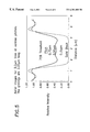
- FIG. 5 is a graph showing data corresponding to aerial images for 0.2 micron line lengths at various pitches, according to the present invention.
- FIG. 6 is a graph showing a relationship between line shortening as a function of pitch for 0.2 micron lines in 3.00 micron gratings of various pitches, according to the present invention.
- FIGS. 7A and 7B are graphs showing a relationship between physical line shortening data as a function of duty cycle (line-size/pitch), according to the present invention.
- the present invention may be applied to a variety of semiconductor structures and has been found to be advantageous for use in connection with optical lithography processes for creating semiconductor elements having narrow line widths. While the present invention is not necessarily so limited, an appreciation of various aspects of the invention may be obtained through a discussion of various application examples in such an environment.
- optical lithographic process An important part of semiconductor processing is the capability of the optical lithographic process to assist in forming elements of extremely small geometry.
- optical lithography When using optical lithography to create semiconductor elements such as narrow linewidths, due to diffraction issues, relative line shortening effects are inherent.
- the present invention address these effects by methods and systems arranged to characterize the extent of the effects for a given application, and then calibrate the optical measurements used for imaging structures, including those having relatively narrow linewidths, onto the wafer.
- the following discussion reveals that the characterization of the relative line shortening effects can be obtained through computer simulation or through a more rigorous mask and measure procedure.
- Optical line shortening measurements such as those discussed herein are based on the reflectance of a patterned resist film. Reflection from a grating is affected by diffraction and scattering as the pitch is decreased. Additionally, reflectance of the focus box structure (e.g., FIG. 1 A), is further complicated by profile and end-of-line effects. The optical line shortening measurement of the focus box structure severely over-predicts the actual truncation as measured by a SEM (e.g., FIG. 1 A). For example, where the minimum optical line shortening for a typical set of data is 0.16 ⁇ m, the measurement by a SEM might yield a truncation of 0.04 ⁇ m.
- the reflectance of the focus box pattern and subsequent image capture of the line edges is simulated, in a simplified manner, by observing the diffraction behavior of sub 0.5 ⁇ m lines to optical illumination. For example, simulating the transmission of 500 ⁇ 100 nm broadband coherent light through a binary mask having a sub 0.5 ⁇ m grating of finite length is straight forward. Neglecting scattering and interference effects caused by the resist and substrate, the aerial image at the end of the lines would qualitatively mimic the response of reflected optical light to trends in line size, line length and pitch of the grating.
- the aerial images of 0.25 ⁇ m lines and spaces are simulated with line lengths on the mask from 2.7 ⁇ m to 3.3 ⁇ m.
- Line edge determination by the metrology tool is arbitrary chosen to be the distance at which the aerial image was 75% of its initial value. Consequently, simulated line shortening is the difference in line lengths of a grating and reference solid 3.0 ⁇ m block respectively and, as discussed further below, the simulated line length bias is linear with the length bias used on the mask.
- general responses of the alignment tool to changes in the focus box pattern (such as physical line shortening, pitch and line size of the grating) are readily predicted and the results are used to calibrate the optical alignment tool.
- the optical alignment tool is then used to fabricate the features of the semiconductor devices.
- a grating is drawn as a binary mask with a given pitch, line size and line length.
- An aerial image is simulated at 500 ⁇ 100 nm.
- the line length response of the measuring tool is simulated at constant threshold level of the aerial image.
- An important aspect of the present invention relates to two corrections that are determined to accurately relate optical measurements to the actual line shortening.
- the first is an offset in linearity and, as will be discussed in more detail below, this is a function of the threshold of the optical measuring tool.
- the second correction is due to a pitch effect. Gratings of various pitches with lines of the same length show that the optical response increases with the pitch even though the line length remains constant.
- optical line shortening measurement equipment is calibrated by measuring the linearity offset at constant grating pitch and duty cycle versus line length, and then measuring the pitch effect.
- the order of such measuring is not critical.
- these affects are modeled using aerial image analogy or a more accurate reflection simulation.
- FIG. 2 is a graph showing a relationship between a modeled optical line shortening effect and a mask bias for another specific simulation example application, according to the present invention.
- line shortening is simulated at a 75% threshold for 0.25 ⁇ m line and space gratings, with lengths ranging from 2.7 ⁇ m to 3.3 ⁇ m.
- this threshold can be related to the job setup (e.g., a function of the background light for the wafer and the focus value).
- the reference block is 3.00 ⁇ m and the line length mask bias is the difference between the grating and reference block line lengths.
- Reference to the “threshold” for the particular application can be an important factor.
- the measurements generated by a given optical alignment tool often vary, and are dependent upon a number of factors particular to the application. These factors include, for example, variances in focus values, the qualities and type of substrate, and the responsiveness of the optical alignment tool and its setup parameters for the application. From one application to the next, an offset in linearity typically occurs as a result of these variances. Thus, the linear relationship illustrated in FIG. 2 yields the illustrated data at a 75% threshold, whereas another application impacted by such variances would likely shift the position of the linearity, but without significantly changing its slope.
- FIGS. 3A and 3B show that the offset effect discussed above in connection with FIG. 2 is primarily a threshold effect.
- FIG. 3A shows a simulation of a 0.25 ⁇ m line and a space grating aerial image with a 3.0 ⁇ m length.
- FIGS. 3A and 3B illustrate data taken with the optical alignment equipment setup at four thresholds: 0.5, 0.6, 0.7 and 0.8.
- FIG. 3B indicates that the measured line length is dependent on the threshold used.
- optical line shortening is significantly larger than line shortening as produced using SEM measurements (i.e., physical line shortening). Furthermore, the duty cycle dependence of optical line shortening measurements is significantly steeper than the SEM measurements. This is particularly true at certain pitches, such as a 0.35 ⁇ m pitch in an example application in which the optical line shortening drastically decreases as duty cycle increases above 0.5.
- FIGS. 4A and 4B shows optical and physical line shortening versus pitch at these above-mentioned example line widths. Physical line shortening decreases or remains relatively stable as pitch increases (FIG. 4 B). However, optical line shortening has the opposite effect by increasing with pitch at constant line width.
- line shortening determined optically changes depending on the duty cycle of the lines in the grating.
- the spacing between the lines, versus the width of the lines also effects the accuracy of the optical measurements and should also be taken into account, in a conventional linear regression analysis, along with the relationships pertaining to pitch and grating length.
- One approach for determining the duty cycle effect is to obtain optical measurements using a mask with lines having constant pitch and grating length, but with varying duty cycles. Data is then gathered, for example, using a SEM for measuring the physical implementation, and this data is compared with the corresponding optical measurements. Using a linear regression analysis, the relationship between the optical measurements and the physical measurements are also factored in and the optical alignment equipment calibrated accordingly.
- FIG. 7A illustrates optical versus physical line shortening data as a function of duty cycle (line-size/pitch).
- FIG. 7B is the corresponding graph of line shortening determined by SEM measurements versus duty cycle.
- FIGS. 7A and 7B show that optical and physical line shortening decreases as duty cycle increases. For convenience, exposure can be used to adjust duty cycle rather than separate masks with various duty cycles. Consequently, for the exemplary application shown, line shortening and duty cycle are closely correlated as shown in FIG. 7 B.
- optical line shortening is significantly larger than line shortening found via SEM measurements (i.e., physical line shortening). Furthermore, the duty cycle dependence of optical line shortening measurements is significantly steeper than the SEM measurements. This is particularly true at 0.35 ⁇ m pitch in which the optical line shortening drastically decreases as duty cycle increased above 0.5.
- the graph of FIG. 2 illustrates the change in line shortening as determined from threshold measurements against the change in grating length. While the slope is near unity, there is a nonzero intercept. This indicates a systematic correction in optical line shortening measurements due to the threshold at the line edge used to determine its length. It has been discovered in connection with the present invention that this intercept can vary with the effective threshold and physically is a function of, for example, the job setup and/or the substrate.
- Optical measurements for these errors are correctable if the response of the optical metrology tool to edge threshold is sufficiently well known.
- there is a correlation between physical and optical line shortening measurements (as in FIG. 9 of Appendix).
- line shortening measurements determined optically are reasonably linear with the physical implementation.
- relative line shortening between two resists at the same line size and pitch are determined, and the line shortening of a particular feature is monitored.
- optical line shortening measurement equipment is calibrated by comparing a series of focus boxes whose grating line width and spacing is fixed but whose length varies by known biases. Optical line shortening measurements are compared to the grating lengths to obtain the calibration curve shown in FIG. 2 .
- a series of focus boxes whose gratings have the same line width and line length but at various pitches. This yields a calibration curve such as shown in FIG. 6 .
- the physical implementation is then compared to the optical.
- lines that are sufficiently large e.g., 0.40 ⁇ m lines and spaces
- lines that are sufficiently large e.g., 0.40 ⁇ m lines and spaces
- the actual line shortening may be small, the optical offset and pitch effect remain.
- a SEM measurement feature for line shortening can be optionally included in a SEM line shortening measurement feature strategically placed, for example, using a comer of the solid portion of the focus box of FIG. 1 A.
- the present invention provides an arrangement and method for calibrating optical alignment equipment to overcome the inherent over-estimates of actual line shortening obtained with optical metrology instruments.
- This calibration is made as a function of pitch effect and a relationship that is determined empirically or via simulations. It is also useful to make this calibration as a function of the relationship between physical line shortening and duty cycle (line-size/pitch). By taking the effect of these three effects in a linear regression analysis, calibration of the optical alignment equipment will be much more accurate.
Landscapes
- Physics & Mathematics (AREA)
- General Physics & Mathematics (AREA)
- Exposure And Positioning Against Photoresist Photosensitive Materials (AREA)
Abstract
Description
Claims (23)
Priority Applications (1)
| Application Number | Priority Date | Filing Date | Title |
|---|---|---|---|
| US09/264,742 US6301008B1 (en) | 1997-03-27 | 1999-03-08 | Arrangement and method for calibrating optical line shortening measurements |
Applications Claiming Priority (3)
| Application Number | Priority Date | Filing Date | Title |
|---|---|---|---|
| US08/826,482 US5902703A (en) | 1997-03-27 | 1997-03-27 | Method for measuring dimensional anomalies in photolithographed integrated circuits using overlay metrology, and masks therefor |
| US08/951,396 US5962173A (en) | 1997-03-27 | 1997-10-16 | Method for measuring the effectiveness of optical proximity corrections |
| US09/264,742 US6301008B1 (en) | 1997-03-27 | 1999-03-08 | Arrangement and method for calibrating optical line shortening measurements |
Related Parent Applications (1)
| Application Number | Title | Priority Date | Filing Date |
|---|---|---|---|
| US08/951,396 Continuation-In-Part US5962173A (en) | 1997-03-27 | 1997-10-16 | Method for measuring the effectiveness of optical proximity corrections |
Publications (1)
| Publication Number | Publication Date |
|---|---|
| US6301008B1 true US6301008B1 (en) | 2001-10-09 |
Family
ID=46256322
Family Applications (1)
| Application Number | Title | Priority Date | Filing Date |
|---|---|---|---|
| US09/264,742 Expired - Fee Related US6301008B1 (en) | 1997-03-27 | 1999-03-08 | Arrangement and method for calibrating optical line shortening measurements |
Country Status (1)
| Country | Link |
|---|---|
| US (1) | US6301008B1 (en) |
Cited By (17)
| Publication number | Priority date | Publication date | Assignee | Title |
|---|---|---|---|---|
| US20030139833A1 (en) * | 1998-02-05 | 2003-07-24 | Micron Technology, Inc. | Methods and apparatus for determining optimum exposure threshold for a given photolithographic model |
| US6602728B1 (en) * | 2001-01-05 | 2003-08-05 | International Business Machines Corporation | Method for generating a proximity model based on proximity rules |
| US20030232253A1 (en) * | 2002-06-18 | 2003-12-18 | Pierre Leroux | Techniques to characterize iso-dense effects for microdevice manufacture |
| US20040101790A1 (en) * | 2002-11-27 | 2004-05-27 | John Cauchi | Photolithography method including a double exposure/double bake |
| US6753116B2 (en) | 2002-01-25 | 2004-06-22 | Mosel Vitelic, Inc. | Multiple photolithographic exposures with different non-clear patterns |
| US6777168B2 (en) | 2001-12-14 | 2004-08-17 | Mosel Vitelic, Inc. | Multiple photolithographic exposures with different clear patterns |
| US20040170905A1 (en) * | 2003-02-28 | 2004-09-02 | International Business Machines Corporation | Binary OPC for assist feature layout optimization |
| US6850858B1 (en) * | 2001-07-06 | 2005-02-01 | Dupont Photomasks, Inc. | Method and apparatus for calibrating a metrology tool |
| US20050250026A1 (en) * | 2004-05-07 | 2005-11-10 | Koninklijke Philips Electronics N.V. | Overlay box structure for measuring process induced line shortening effect |
| US20060080046A1 (en) * | 2004-10-13 | 2006-04-13 | David Ziger | Measuring flare in semiconductor lithography |
| US20060210885A1 (en) * | 2003-08-01 | 2006-09-21 | David Ziger | Measuring the effect of flare on line width |
| US20070275329A1 (en) * | 2003-04-29 | 2007-11-29 | Koninklijke Philips Electronics N.V. | System and Method for Characterizing Lithography Effects on a Wafer |
| US20080174778A1 (en) * | 2007-01-23 | 2008-07-24 | Taiwan Semiconductor Manufacturing Company, Ltd. | Method and System For Optimizing Sub-Nanometer Critical Dimension Using Pitch Offset |
| US20080290264A1 (en) * | 2005-11-02 | 2008-11-27 | Fei Company | Corrector for the correction of chromatic aberrations in a particle-optical apparatus |
| US7541121B2 (en) | 2004-10-13 | 2009-06-02 | Infineon Technologies Ag | Calibration of optical line shortening measurements |
| US8569693B2 (en) | 2011-04-13 | 2013-10-29 | Fei Company | Distortion free stigmation of a TEM |
| US9983154B2 (en) | 2015-12-14 | 2018-05-29 | Imec Vzw | Method for inspecting a pattern of features on a semiconductor die |
Citations (1)
| Publication number | Priority date | Publication date | Assignee | Title |
|---|---|---|---|---|
| US5629772A (en) * | 1994-12-20 | 1997-05-13 | International Business Machines Corporation | Monitoring of minimum features on a substrate |
-
1999
- 1999-03-08 US US09/264,742 patent/US6301008B1/en not_active Expired - Fee Related
Patent Citations (1)
| Publication number | Priority date | Publication date | Assignee | Title |
|---|---|---|---|---|
| US5629772A (en) * | 1994-12-20 | 1997-05-13 | International Business Machines Corporation | Monitoring of minimum features on a substrate |
Non-Patent Citations (9)
| Title |
|---|
| C.P. Ausschnitt and M.E. Lagus, "Seeing the forest for the trees: a new approach to CD control," Proceedings of the SPIE, 3332, pp. 212-220 (1998). |
| D.H. Ziger, T.E. Adams, and J. Garofallo, "Linesize effects on ultraviolet reflectance spectra," Opt. Eng., 36, pp 243-250 (1997). |
| E. Barouch, U. Hollerbach and R. Vallishayee, "OPTIMASK: An OPC Algorithm for Chrome and Phase-Shift Mask Design," Proc SPIE 2440, 1992-206 (1995). |
| M. Sugawara, H. Kawahira, K. Tsudaka and S. Nozawa, "Practical evaluation of optical proximity effect correction by EDM methodology," Proc SPIE 2440, 207-219 (1995). |
| O.W. Otto and R.C. Henderson, "Integrating proximity effects corrections with photomask data preparation," Proc SPIE 2440, 184-191 (1995). |
| R. Pforr, et al., "Feature biasing versus feature-assisted lithography-a comparison of proximity corrections," Proc SPIE 2440, 150-170 (1995). |
| T.A. Brunner, "New focus metrology technique using special test mask," OCG Interface (1993), pp 1-9. |
| T.A. Brunner, T.L. Martin, R.M. Martino, C.P. Ausschnitt and T.H. Newman, "Quantitative stepper metrology using focus monitor test mask," Proc SPIE 2197, 541-549 (1994). |
| T.E. Adams, "Applications of latent image metrology in microlithography," Proc SPIE 1464, 294-303 (1991). |
Cited By (33)
| Publication number | Priority date | Publication date | Assignee | Title |
|---|---|---|---|---|
| US20030139833A1 (en) * | 1998-02-05 | 2003-07-24 | Micron Technology, Inc. | Methods and apparatus for determining optimum exposure threshold for a given photolithographic model |
| US6602728B1 (en) * | 2001-01-05 | 2003-08-05 | International Business Machines Corporation | Method for generating a proximity model based on proximity rules |
| US6850858B1 (en) * | 2001-07-06 | 2005-02-01 | Dupont Photomasks, Inc. | Method and apparatus for calibrating a metrology tool |
| US6777168B2 (en) | 2001-12-14 | 2004-08-17 | Mosel Vitelic, Inc. | Multiple photolithographic exposures with different clear patterns |
| US6753116B2 (en) | 2002-01-25 | 2004-06-22 | Mosel Vitelic, Inc. | Multiple photolithographic exposures with different non-clear patterns |
| US20030232253A1 (en) * | 2002-06-18 | 2003-12-18 | Pierre Leroux | Techniques to characterize iso-dense effects for microdevice manufacture |
| US6800403B2 (en) | 2002-06-18 | 2004-10-05 | Koninklijke Philips Electronics N.V. | Techniques to characterize iso-dense effects for microdevice manufacture |
| US6881524B2 (en) | 2002-11-27 | 2005-04-19 | Promos Technologies, Inc. | Photolithography method including a double exposure/double bake |
| US20040101790A1 (en) * | 2002-11-27 | 2004-05-27 | John Cauchi | Photolithography method including a double exposure/double bake |
| US7147976B2 (en) | 2003-02-28 | 2006-12-12 | International Business Machines Corporation | Binary OPC for assist feature layout optimization |
| US7001693B2 (en) | 2003-02-28 | 2006-02-21 | International Business Machines Corporation | Binary OPC for assist feature layout optimization |
| US20060057475A1 (en) * | 2003-02-28 | 2006-03-16 | Liebmann Lars W | Binary OPC for assist feature layout optimization |
| US20040170905A1 (en) * | 2003-02-28 | 2004-09-02 | International Business Machines Corporation | Binary OPC for assist feature layout optimization |
| US7537939B2 (en) | 2003-04-29 | 2009-05-26 | Nxp B.V. | System and method for characterizing lithography effects on a wafer |
| US20070275329A1 (en) * | 2003-04-29 | 2007-11-29 | Koninklijke Philips Electronics N.V. | System and Method for Characterizing Lithography Effects on a Wafer |
| US7556900B2 (en) | 2003-08-01 | 2009-07-07 | Nxp B.V. | Measuring the effect of flare on line width |
| US20060210885A1 (en) * | 2003-08-01 | 2006-09-21 | David Ziger | Measuring the effect of flare on line width |
| US20050250026A1 (en) * | 2004-05-07 | 2005-11-10 | Koninklijke Philips Electronics N.V. | Overlay box structure for measuring process induced line shortening effect |
| US7332255B2 (en) * | 2004-05-07 | 2008-02-19 | Nxp B.V. | Overlay box structure for measuring process induced line shortening effect |
| US7096127B2 (en) | 2004-10-13 | 2006-08-22 | Infineon Technologies Ag | Measuring flare in semiconductor lithography |
| US8717539B2 (en) | 2004-10-13 | 2014-05-06 | Infineon Technologies Ag | Calibration of optical line shortening measurements |
| US20110035171A1 (en) * | 2004-10-13 | 2011-02-10 | David Ziger | Calibration of Optical Line Shortening Measurements |
| US7541121B2 (en) | 2004-10-13 | 2009-06-02 | Infineon Technologies Ag | Calibration of optical line shortening measurements |
| US20060080046A1 (en) * | 2004-10-13 | 2006-04-13 | David Ziger | Measuring flare in semiconductor lithography |
| US20090198468A1 (en) * | 2004-10-13 | 2009-08-06 | David Ziger | Calibration of Optical Line Shortening Measurements |
| DE112005002263B4 (en) | 2004-10-13 | 2011-03-17 | Infineon Technologies Ag | Calibration of optical line shortening measurements |
| US7842439B2 (en) | 2004-10-13 | 2010-11-30 | Infineon Technologies Ag | Calibration of optical line shortening measurements |
| US20080290264A1 (en) * | 2005-11-02 | 2008-11-27 | Fei Company | Corrector for the correction of chromatic aberrations in a particle-optical apparatus |
| US8884245B2 (en) | 2005-11-02 | 2014-11-11 | Fei Company | Corrector for the correction of chromatic aberrations in a particle-optical apparatus |
| US7777884B2 (en) * | 2007-01-23 | 2010-08-17 | Taiwan Semiconductor Manufacturing Company, Ltd. | Method and system for optimizing sub-nanometer critical dimension using pitch offset |
| US20080174778A1 (en) * | 2007-01-23 | 2008-07-24 | Taiwan Semiconductor Manufacturing Company, Ltd. | Method and System For Optimizing Sub-Nanometer Critical Dimension Using Pitch Offset |
| US8569693B2 (en) | 2011-04-13 | 2013-10-29 | Fei Company | Distortion free stigmation of a TEM |
| US9983154B2 (en) | 2015-12-14 | 2018-05-29 | Imec Vzw | Method for inspecting a pattern of features on a semiconductor die |
Similar Documents
| Publication | Publication Date | Title |
|---|---|---|
| US6301008B1 (en) | Arrangement and method for calibrating optical line shortening measurements | |
| US11675277B2 (en) | Self-referencing and self-calibrating interference pattern overlay measurement | |
| KR100301648B1 (en) | Metrology method using tone-reversing pattern | |
| KR100276852B1 (en) | Feature size control system using tone reversing patterns | |
| KR100276849B1 (en) | Optically measurable serpentine edge tone reversed targets | |
| KR100216143B1 (en) | Improved photolithography mask | |
| US7396621B2 (en) | Exposure control method and method of manufacturing a semiconductor device | |
| US6498640B1 (en) | Method to measure alignment using latent image grating structures | |
| US7327436B2 (en) | Method for evaluating a local flare, correction method for a mask pattern, manufacturing method for a semiconductor device and a computer program product | |
| CN101937904B (en) | Semiconductor device and method of manufacturing the same | |
| US8717539B2 (en) | Calibration of optical line shortening measurements | |
| KR20020068324A (en) | Method and System for Selective Linewidth Optimization During a Lithographic Process | |
| KR19990083365A (en) | Semiconductor manufacturing method and manufacturing apparatus, and semiconductor device being manufactured thereby | |
| US7349105B2 (en) | Method and apparatus for measuring alignment of layers in photolithographic processes | |
| US5723238A (en) | Inspection of lens error associated with lens heating in a photolithographic system | |
| US7476473B2 (en) | Process control method, a method for forming monitor marks, a mask for process control, and a semiconductor device manufacturing method | |
| JP2991661B2 (en) | Semiconductor device process defect inspection method | |
| JP2797362B2 (en) | Semiconductor device pattern forming method | |
| US7186484B2 (en) | Method for determining the relative positional accuracy of two structure elements on a wafer | |
| US20030203288A1 (en) | Overlay measuring pattern, photomask, and overlay measuring method and apparatus | |
| US5616438A (en) | Reticle and a method for measuring blind setting accuracy using the same | |
| Ziger et al. | Understanding optical end of line metrology | |
| KR100355771B1 (en) | Method for measuring a pattern displacement in a photomasking process | |
| KR20000031429A (en) | Mask pattern of semiconductor exposure apparatus and method for estimating pattern shift of the same | |
| US20080070416A1 (en) | Phase shift mask including a substrate with recess |
Legal Events
| Date | Code | Title | Description |
|---|---|---|---|
| AS | Assignment |
Owner name: VLSI TECHNOLOGY, INC., CALIFORNIA Free format text: ASSIGNMENT OF ASSIGNORS INTEREST;ASSIGNORS:ZIGER, DAVID;LEROUX, PIERRE;REEL/FRAME:010181/0073 Effective date: 19990517 |
|
| REMI | Maintenance fee reminder mailed | ||
| FPAY | Fee payment |
Year of fee payment: 4 |
|
| SULP | Surcharge for late payment | ||
| AS | Assignment |
Owner name: PHILIPS SEMICONDUCTORS VLSI INC., NEW YORK Free format text: CHANGE OF NAME;ASSIGNOR:VLSI TECHNOLOGY, INC.;REEL/FRAME:018635/0570 Effective date: 19990702 Owner name: NXP B.V., NETHERLANDS Free format text: ASSIGNMENT OF ASSIGNORS INTEREST;ASSIGNOR:PHILIPS SEMICONDUCTORS INC.;REEL/FRAME:018645/0779 Effective date: 20061130 |
|
| AS | Assignment |
Owner name: PHILIPS SEMICONDUCTORS INC., NEW YORK Free format text: CHANGE OF NAME;ASSIGNOR:PHILIPS SEMICONDUCTORS VLSI INC.;REEL/FRAME:018668/0255 Effective date: 19991220 |
|
| FPAY | Fee payment |
Year of fee payment: 8 |
|
| REMI | Maintenance fee reminder mailed | ||
| LAPS | Lapse for failure to pay maintenance fees | ||
| STCH | Information on status: patent discontinuation |
Free format text: PATENT EXPIRED DUE TO NONPAYMENT OF MAINTENANCE FEES UNDER 37 CFR 1.362 |
|
| FP | Lapsed due to failure to pay maintenance fee |
Effective date: 20131009 |