US6285322B1 - Electronics unit for wireless transfer of signals - Google Patents
Electronics unit for wireless transfer of signals Download PDFInfo
- Publication number
- US6285322B1 US6285322B1 US09/002,369 US236998A US6285322B1 US 6285322 B1 US6285322 B1 US 6285322B1 US 236998 A US236998 A US 236998A US 6285322 B1 US6285322 B1 US 6285322B1
- Authority
- US
- United States
- Prior art keywords
- antenna
- electronics
- electronics unit
- unit according
- substrate layer
- Prior art date
- Legal status (The legal status is an assumption and is not a legal conclusion. Google has not performed a legal analysis and makes no representation as to the accuracy of the status listed.)
- Expired - Lifetime
Links
Images


Classifications
-
- H—ELECTRICITY
- H01—ELECTRIC ELEMENTS
- H01Q—ANTENNAS, i.e. RADIO AERIALS
- H01Q21/00—Antenna arrays or systems
- H01Q21/06—Arrays of individually energised antenna units similarly polarised and spaced apart
- H01Q21/20—Arrays of individually energised antenna units similarly polarised and spaced apart the units being spaced along or adjacent to a curvilinear path
- H01Q21/205—Arrays of individually energised antenna units similarly polarised and spaced apart the units being spaced along or adjacent to a curvilinear path providing an omnidirectional coverage
-
- H—ELECTRICITY
- H01—ELECTRIC ELEMENTS
- H01Q—ANTENNAS, i.e. RADIO AERIALS
- H01Q1/00—Details of, or arrangements associated with, antennas
- H01Q1/36—Structural form of radiating elements, e.g. cone, spiral, umbrella; Particular materials used therewith
- H01Q1/38—Structural form of radiating elements, e.g. cone, spiral, umbrella; Particular materials used therewith formed by a conductive layer on an insulating support
-
- H—ELECTRICITY
- H01—ELECTRIC ELEMENTS
- H01Q—ANTENNAS, i.e. RADIO AERIALS
- H01Q23/00—Antennas with active circuits or circuit elements integrated within them or attached to them
-
- H—ELECTRICITY
- H01—ELECTRIC ELEMENTS
- H01Q—ANTENNAS, i.e. RADIO AERIALS
- H01Q9/00—Electrically-short antennas having dimensions not more than twice the operating wavelength and consisting of conductive active radiating elements
- H01Q9/04—Resonant antennas
- H01Q9/0407—Substantially flat resonant element parallel to ground plane, e.g. patch antenna
- H01Q9/0471—Non-planar, stepped or wedge-shaped patch
Definitions
- the present invention relates to an electronics unit for wireless transfer of signals, which comprises an antenna part, transmission circuits and an electronics part.
- the unit is based on a laminate with a substrate layer of a dielectric material.
- Microstrip technology is a microwave technology which is based on laminates of two electrically conducting layers, and an intermediate dielectric layer. This dielectric layer is also called substrate, and serves not only as an isolating layer, but also as mechanical support for the electrically conducting layers.
- Previously known electronics units for the transfer of signals within a large angle divided into sectors consist of a separate electronics part and a separate antenna part, between which there are transmission circuits in the form of conventional cables. These are connected to each part by means of soldering or connectors. This previously known technology is expensive, and demands a great deal of space, and can cause interruptions in operation due to manufacturing errors, ageing, etc.
- the object of the present invention is to obtain an electronics unit which is simple, cost efficient, saves space and provides good characteristics, since the invention solves the interface problems between the antenna part and the electronics part.
- an electronics unit is characterized by a construction with substrate layers which are divided into three continuous sections, which are a first section which is part of the electronics part, a second section which forms the substrate in the antenna part, and a third section which supports the transmission circuits.
- the substrate extends continuously between the three sections, and is made of a flexible material, and is in the third section bent to a curved form. Its convex surface supports radiation elements, the beams of which, due to the bent surface, point in different directions.
- an integrated unit is obtained with one and the same construction, and without intermediate organs such as solderings or connectors.
- FIGS. 1 and 2 show different perspective views of the electronics unit in one example of an embodiment
- FIG. 3 shows an opened view of the electronics unit
- FIG. 4 shows a side-view of the opened electronics unit
- FIG. 5 shows a cross-section through the antenna part in the electronics unit
- FIG. 6 schematically shows the construction of the antenna part.
- the antenna unit according to the invention consists of an electronics part 1 , an antenna part 2 , and a transmission circuit part 3 with transmission circuits 3 which form the interface between the electronics part and the antenna part.
- both the electronics part 1 , the antenna part 2 , and the transmission circuit part 3 are designed using the same construction, i.e. microstrip technology with a supporting structure, which according to the invention is a substrate which is common to both the electronics part 1 , the antenna part 2 and the transmission circuit part 3 .
- the antenna part 2 is of the conformal sector antenna kind, with a plurality of evenly spaced antenna elements 5 , 6 , 7 , 8 , 9 , 10 around a cylinder 4 , see also FIG. 5 .
- the antenna is of the so-called multi-sector antenna kind, i.e. the antenna elements are so positioned that they together have a directivity in several (in the example shown, all) directions as seen in a plane which is perpendicular to the longitudinal axis 11 of the cylinder formed.
- the electronics part 1 is in the example shown supported by a substrate 12 , which in connection to the electronics part preferably is plane, and also by a massive supporting structure 13 of metal which forms a base-part in the electronics unit.
- the electronics unit is advantageously shaped with an external contour, which in its entirety is cylindrically shaped, for which reason the base part is shaped with a side section 14 , with a cylindrical enveloping surface which becomes a cylindrical bottom plate 15 , on the bottom side of which connectors can be arranged for the connection of the electronics part to other units in, for example, a base station or a microwave link used for, for example telecommunications such as mobile telephony communication, data communication, video communication or other transfer of signals.
- the substrate in the electronics part 1 can form a supporting structure for analogue/digital electronics such as surface-mounted electronics, microstrip, transmission lines and the like. Said electronics can comprise further laminates.
- the example shown comprises an electronically controlled switch 18 for the connection of one or several of the antenna elements 5 - 10 according to certain chosen criteria for transmission and reception in chosen antenna sectors via each transmission circuit 3 in a manner which as such is known.
- the electrically controlled switch 18 is controlled via a (not shown) control connection.
- the construction according to the invention will in the following be described in more detail.
- the electronics part 1 , the antenna part 2 and the transmission circuit part 3 with the connecting transmission circuits 3 ′ are supported on a continuous common flexible substrate 12 , which is manufactured from, for example, a polymer, for example tetrafluorethylene.
- the laminate also comprises a ground plane 21 across the entire surface of the substrate on one of its sides, and the transmission circuits 3 ′ in the form of microstrip conductors on its other side.
- sections 24 of a second substrate to be more exact one section for each antenna element 5 .
- These substrate sections 24 are spaced apart from each other, and on their outside support antenna elements 5 - 10 , for example so-called patches in the form of copper layers which can exhibit a suitable form, for example a rectangular or circular form.
- the antenna elements can be arranged in groups comprising one or several antenna elements. Due to the curved surface, the groups point in different directions.
- the basic part of the common substrate for the electronics part 1 , the antenna part 2 and the transmission circuit part 3 is a plane substrate piece, which in the example shown essentially is T-shaped, where a part of the “leg” forms a first part 22 of the substrate which serves as a support for the electronics part, and the cross-bar forms a second part 23 of the substrate, which serves as support for the antenna part 2 , and an interface between the first and the second part forms a third part 20 of the substrate, which forms a support for the transmission circuit part 3 .
- the final shape of the antenna part 2 is obtained by bending the cross-bar 23 , i.e. the second part with its ground plane and any other layers.
- the cross-bar is bent to a shape which essentially is cylindrically formed.
- the sections 24 of the second substrate in practice a certain stiffening is obtained of these parts in relation to the intervals 25 which are formed between the sections.
- FIG. 5 shows only arc-shaped lines, the shape can in practice become polygonal, thus causing essentially plane antenna elements 5 - 10 .
- the cross-bar 23 of the substrate piece is dimensioned so that the two outer edges 26 , 27 will essentially meet, to form a closed convex enveloping surface with a chosen diameter.
- the ground plane 21 is bent together with the substrate 12 , so that it, similarly to the substrate, is given a bent shape.
- the ground plane in FIG. 5 is shown as a thick circumferential arc line.
- the ground plane 21 can, similarly to the substrate 20 , be considered to consist of three continuous sections in the form of an electrically conducting layer which extends across both the electronics part 1 , the antenna part 2 and the transmission circuit part 3 .
- This forms the above-mentioned interface, by means of which the transmission circuits extend from the electronics part 1 and into the antenna part 2 , to be more exact one conductor all the way up to a chosen point, at least up to the area of each aperture 35 .
- the antenna part 2 exhibits a body 28 of metal which, in the example shown, has six radially extending walls 29 , 30 which extend from a center which coincides with the axis of symmetry 11 .
- the body 28 due to its design, delimits a chamber 31 behind each antenna element 5 - 10 .
- These chambers 31 suppress radiation in the backwards and side directions, both from the antenna elements and from the transmission circuits 3 , which reduces the problem of interference between the radiating components.
- the chambers also form cavities which affect the impedance adjustment of the antenna element.
- the body 28 has radially outwards facing end surfaces 32 , against which the substrate 20 obtains support with its inside.
- the bent substrate layer can be attached to the end surfaces, for example by means of screws through holes 17 , see FIG. 3 .
- a cover 33 Radially outside of the antenna element 5 - 10 there is arranged a cover 33 , which is tube-shaped and preferably cylindrical, and which is designed in a known manner in a material with low attenuation of electromagnetic waves.
- the cover 33 forms a radome, and also an outer mechanical support and protection for the substrate part 23 of the antenna part which is bent to a convex shape, and which, if it has elastic properties, thus is contained to the predetermined form due to interaction with the body 28 from the inside.
- the radome 33 extends in the direction of the longitudinal axis 11 , at least enough to cover the height of the substrate part 23 .
- the radome can advantageously exhibit a closed end wall above the antenna part 2 , and can also surround the electronics part 1 and the transmission circuit part 3 , which however is not shown.
- FIG. 6 shows the above-mentioned substrate construction with the first substrate 12 , from which it can be seen that the ground plane 21 exhibits oblique slit-shaped openings 35 , so-called apertures which, as such, are previously known, and which form radiation elements in order to transfer the microwave energy from the transmission circuits 3 to the antenna element 5 , which in turn during transmission radiate in an outwards direction in a chosen sector. During reception, the microwave radiation goes in the opposite direction.
- the antenna elements 5 - 10 can have another shape, or their amount can be larger or smaller.
- each antenna element can be extended to a group of radiation elements in the same direction, for example to alter the beam-shape in a plane parallel to the cylinder axis 11 .
- the patches, and thus the second substrate 24 are not a necessary condition in order to carry out the invention. In principle, both the body 28 and the radome 33 can be left out.
Landscapes
- Details Of Aerials (AREA)
- Variable-Direction Aerials And Aerial Arrays (AREA)
- Telephone Set Structure (AREA)
Abstract
An electronics unit for wireless transfer of signals, includes an antenna part, an electronics part, and a transmission circuit part. The electronics part is placed on a laminate with at least one substrate layer of a dielectric material. The substrate layer is made of a flexible material and forms a continuous unit, including a first part which supports the electronics part, a second part which supports the antenna part, and a third part which supports the transmission circuit part. The second part of the substrate is formed to shape a convex surface, which supports groups of at least one antenna element. Since the surface is curved, the groups cover different directions.
Description
The present invention relates to an electronics unit for wireless transfer of signals, which comprises an antenna part, transmission circuits and an electronics part. The unit is based on a laminate with a substrate layer of a dielectric material.
When transferring signals by means of electromagnetic waves at high frequencies, to be more exact within the microwave area, microstrip technology is used both for the antenna part and the electronics part. Microstrip technology is a microwave technology which is based on laminates of two electrically conducting layers, and an intermediate dielectric layer. This dielectric layer is also called substrate, and serves not only as an isolating layer, but also as mechanical support for the electrically conducting layers. Previously known electronics units for the transfer of signals within a large angle divided into sectors consist of a separate electronics part and a separate antenna part, between which there are transmission circuits in the form of conventional cables. These are connected to each part by means of soldering or connectors. This previously known technology is expensive, and demands a great deal of space, and can cause interruptions in operation due to manufacturing errors, ageing, etc.
The object of the present invention is to obtain an electronics unit which is simple, cost efficient, saves space and provides good characteristics, since the invention solves the interface problems between the antenna part and the electronics part.
The said object is achieved by means of an electronics unit according to the present invention. This is characterized by a construction with substrate layers which are divided into three continuous sections, which are a first section which is part of the electronics part, a second section which forms the substrate in the antenna part, and a third section which supports the transmission circuits. The substrate extends continuously between the three sections, and is made of a flexible material, and is in the third section bent to a curved form. Its convex surface supports radiation elements, the beams of which, due to the bent surface, point in different directions.
Due to the construction according to the invention, an integrated unit is obtained with one and the same construction, and without intermediate organs such as solderings or connectors.
The invention will in the following be described in closer detail using an example of an embodiment with reference to the appended drawings, in which:
FIGS. 1 and 2 show different perspective views of the electronics unit in one example of an embodiment,
FIG. 3 shows an opened view of the electronics unit,
FIG. 4 shows a side-view of the opened electronics unit, and
FIG. 5 shows a cross-section through the antenna part in the electronics unit, and
FIG. 6 schematically shows the construction of the antenna part.
As can best be seen in FIGS. 1 and 2, the antenna unit according to the invention consists of an electronics part 1, an antenna part 2, and a transmission circuit part 3 with transmission circuits 3 which form the interface between the electronics part and the antenna part. According to the invention, both the electronics part 1, the antenna part 2, and the transmission circuit part 3 are designed using the same construction, i.e. microstrip technology with a supporting structure, which according to the invention is a substrate which is common to both the electronics part 1, the antenna part 2 and the transmission circuit part 3. The antenna part 2 is of the conformal sector antenna kind, with a plurality of evenly spaced antenna elements 5, 6, 7, 8, 9, 10 around a cylinder 4, see also FIG. 5. The antenna is of the so-called multi-sector antenna kind, i.e. the antenna elements are so positioned that they together have a directivity in several (in the example shown, all) directions as seen in a plane which is perpendicular to the longitudinal axis 11 of the cylinder formed.
The electronics part 1 is in the example shown supported by a substrate 12, which in connection to the electronics part preferably is plane, and also by a massive supporting structure 13 of metal which forms a base-part in the electronics unit. The electronics unit is advantageously shaped with an external contour, which in its entirety is cylindrically shaped, for which reason the base part is shaped with a side section 14, with a cylindrical enveloping surface which becomes a cylindrical bottom plate 15, on the bottom side of which connectors can be arranged for the connection of the electronics part to other units in, for example, a base station or a microwave link used for, for example telecommunications such as mobile telephony communication, data communication, video communication or other transfer of signals. The substrate in the electronics part 1 can form a supporting structure for analogue/digital electronics such as surface-mounted electronics, microstrip, transmission lines and the like. Said electronics can comprise further laminates. The example shown comprises an electronically controlled switch 18 for the connection of one or several of the antenna elements 5-10 according to certain chosen criteria for transmission and reception in chosen antenna sectors via each transmission circuit 3 in a manner which as such is known. The electrically controlled switch 18 is controlled via a (not shown) control connection.
With reference to FIGS. 4, 5 and 6, the construction according to the invention will in the following be described in more detail. As mentioned above, the electronics part 1, the antenna part 2 and the transmission circuit part 3 with the connecting transmission circuits 3′, are supported on a continuous common flexible substrate 12, which is manufactured from, for example, a polymer, for example tetrafluorethylene. The laminate also comprises a ground plane 21 across the entire surface of the substrate on one of its sides, and the transmission circuits 3′ in the form of microstrip conductors on its other side. In the antenna part, there are arranged sections 24 of a second substrate, to be more exact one section for each antenna element 5. These substrate sections 24 are spaced apart from each other, and on their outside support antenna elements 5-10, for example so-called patches in the form of copper layers which can exhibit a suitable form, for example a rectangular or circular form. The antenna elements can be arranged in groups comprising one or several antenna elements. Due to the curved surface, the groups point in different directions.
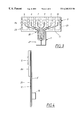
As can be seen in FIG. 3, the basic part of the common substrate for the electronics part 1, the antenna part 2 and the transmission circuit part 3 is a plane substrate piece, which in the example shown essentially is T-shaped, where a part of the “leg” forms a first part 22 of the substrate which serves as a support for the electronics part, and the cross-bar forms a second part 23 of the substrate, which serves as support for the antenna part 2, and an interface between the first and the second part forms a third part 20 of the substrate, which forms a support for the transmission circuit part 3. The final shape of the antenna part 2 is obtained by bending the cross-bar 23, i.e. the second part with its ground plane and any other layers. In the example shown the cross-bar is bent to a shape which essentially is cylindrically formed. By means of a certain reduced elasticity in the sections 24 of the second substrate, in practice a certain stiffening is obtained of these parts in relation to the intervals 25 which are formed between the sections. Although FIG. 5, for reasons of simplicity, shows only arc-shaped lines, the shape can in practice become polygonal, thus causing essentially plane antenna elements 5-10. The cross-bar 23 of the substrate piece is dimensioned so that the two outer edges 26, 27 will essentially meet, to form a closed convex enveloping surface with a chosen diameter. The ground plane 21 is bent together with the substrate 12, so that it, similarly to the substrate, is given a bent shape. For reasons of simplicity, the ground plane in FIG. 5 is shown as a thick circumferential arc line.
One and the same substrate layer 12 thus forms a continuous supporting structure both for the electronics part 1, the antenna part, and the transmission circuits 3′ of the transmission circuit part 3 which extend between them. The ground plane 21 can, similarly to the substrate 20, be considered to consist of three continuous sections in the form of an electrically conducting layer which extends across both the electronics part 1, the antenna part 2 and the transmission circuit part 3. This forms the above-mentioned interface, by means of which the transmission circuits extend from the electronics part 1 and into the antenna part 2, to be more exact one conductor all the way up to a chosen point, at least up to the area of each aperture 35.
As can be seen in FIG. 5, the antenna part 2 exhibits a body 28 of metal which, in the example shown, has six radially extending walls 29, 30 which extend from a center which coincides with the axis of symmetry 11. The body 28, due to its design, delimits a chamber 31 behind each antenna element 5-10. These chambers 31 suppress radiation in the backwards and side directions, both from the antenna elements and from the transmission circuits 3, which reduces the problem of interference between the radiating components. The chambers also form cavities which affect the impedance adjustment of the antenna element. The body 28 has radially outwards facing end surfaces 32, against which the substrate 20 obtains support with its inside. The bent substrate layer can be attached to the end surfaces, for example by means of screws through holes 17, see FIG. 3.
Radially outside of the antenna element 5-10 there is arranged a cover 33, which is tube-shaped and preferably cylindrical, and which is designed in a known manner in a material with low attenuation of electromagnetic waves. The cover 33 forms a radome, and also an outer mechanical support and protection for the substrate part 23 of the antenna part which is bent to a convex shape, and which, if it has elastic properties, thus is contained to the predetermined form due to interaction with the body 28 from the inside. The radome 33 extends in the direction of the longitudinal axis 11, at least enough to cover the height of the substrate part 23. The radome can advantageously exhibit a closed end wall above the antenna part 2, and can also surround the electronics part 1 and the transmission circuit part 3, which however is not shown.
FIG. 6 shows the above-mentioned substrate construction with the first substrate 12, from which it can be seen that the ground plane 21 exhibits oblique slit-shaped openings 35, so-called apertures which, as such, are previously known, and which form radiation elements in order to transfer the microwave energy from the transmission circuits 3 to the antenna element 5, which in turn during transmission radiate in an outwards direction in a chosen sector. During reception, the microwave radiation goes in the opposite direction.
The invention is not limited to the examples of embodiments described above and shown in the figures, but can be varied within the scope of the appended claims. For example, the antenna elements 5-10 can have another shape, or their amount can be larger or smaller. Furthermore, each antenna element can be extended to a group of radiation elements in the same direction, for example to alter the beam-shape in a plane parallel to the cylinder axis 11. Furthermore, the patches, and thus the second substrate 24 are not a necessary condition in order to carry out the invention. In principle, both the body 28 and the radome 33 can be left out.
Claims (11)
1. An electronics unit for wireless transfer of signals comprising an antenna part, an electronics part which is constructed on a laminate with at least one substrate layer of a dielectric material, and a transmission circuit part with transmission circuits which connect the electronics part to the antenna part, wherein said substrate layer is made from a flexible material, and the substrate layer forms one common continuous unit which comprises a first section which supports said electronics part, a second section which supports said antenna part, and a third section which supports said transmission circuit part, and wherein said second section of the substrate is bent to a curved shape, a convex surface of which supports groups of antennae comprising at least one antenna element each, which groups of antennae point in different directions due to the convex surface.
2. The electronics unit according to claim 1, wherein the antenna part forms an outwardly closed surface.
3. The electronics unit according to claim 2, wherein the antenna part exhibits a substantially cylindrical shape.
4. The electronics unit according to claim 3, wherein the antenna elements are placed around said convex surface so that their beams cover the circumference.
5. The electronics unit according to claim 1, wherein the antenna element and the transmission circuits are designed in microstrip technology.
6. The electronics unit according to claim 5, wherein said substrate supports a ground plane, which continuously extends across the electronics part, the transmission part, and the antenna part.
7. The electronics unit according to claim 6, wherein the antenna part exhibits apertures in the ground plane.
8. The electronics unit according to claim 7, wherein the antenna part exhibits antenna elements positioned outside of the apertures, which antenna elements are in the form of microstrip elements on a second substrate layer.
9. The electronics unit according to claim 4, wherein the second section of said substrate layer is bent around a metal body with radially directed separating walls.
10. The electronics unit according to claim 4, wherein at least the second section of said substrate layer with antenna elements is contained by a substantially cylindrical radome which serves both as mechanical support and as protection for the antenna part.
11. The electronics unit of claim 1, wherein the first, second and third sections are arranged consecutively on the substrate layer.
Applications Claiming Priority (2)
| Application Number | Priority Date | Filing Date | Title |
|---|---|---|---|
| SE9700029A SE508297C2 (en) | 1997-01-03 | 1997-01-03 | Electronic unit for wireless signal transmission |
| SE9700029 | 1997-01-03 |
Publications (1)
| Publication Number | Publication Date |
|---|---|
| US6285322B1 true US6285322B1 (en) | 2001-09-04 |
Family
ID=20405368
Family Applications (1)
| Application Number | Title | Priority Date | Filing Date |
|---|---|---|---|
| US09/002,369 Expired - Lifetime US6285322B1 (en) | 1997-01-03 | 1998-01-02 | Electronics unit for wireless transfer of signals |
Country Status (8)
| Country | Link |
|---|---|
| US (1) | US6285322B1 (en) |
| EP (1) | EP0965150B1 (en) |
| JP (1) | JP3803976B2 (en) |
| CN (1) | CN1108642C (en) |
| AU (1) | AU5582798A (en) |
| DE (1) | DE69733036T2 (en) |
| SE (1) | SE508297C2 (en) |
| WO (1) | WO1998029920A1 (en) |
Cited By (9)
| Publication number | Priority date | Publication date | Assignee | Title |
|---|---|---|---|---|
| USD481029S1 (en) | 2002-02-04 | 2003-10-21 | Mitsumi Electric Co., Ltd. | Loop antenna |
| USD484117S1 (en) | 2002-06-20 | 2003-12-23 | Mitsumi Electric Co., Ltd. | Loop antenna |
| USD484119S1 (en) | 2002-06-20 | 2003-12-23 | Mitsumi Electric Co., Ltd. | Loop antenna |
| US6693595B2 (en) * | 2002-04-25 | 2004-02-17 | Southern Methodist University | Cylindrical double-layer microstrip array antenna |
| EP1559168A4 (en) * | 2002-11-04 | 2006-02-15 | Ipr Licensing Inc | Folding directional antenna |
| WO2010050892A1 (en) * | 2008-10-30 | 2010-05-06 | Nanyang Polytechnic | Compact tunable diversity antenna |
| EP2389709B1 (en) * | 2009-01-20 | 2015-01-28 | Raytheon Company | Integrated patch antenna |
| EP3462536A1 (en) * | 2017-10-02 | 2019-04-03 | Nokia Shanghai Bell Co. Ltd. | Compact antenna |
| EP3840119A1 (en) * | 2019-12-19 | 2021-06-23 | Valeo Comfort and Driving Assistance | Automotive mimo antenna system for 5g standard and beyond |
Families Citing this family (5)
| Publication number | Priority date | Publication date | Assignee | Title |
|---|---|---|---|---|
| US7345632B2 (en) | 2003-02-12 | 2008-03-18 | Nortel Networks Limited | Multibeam planar antenna structure and method of fabrication |
| US6879291B2 (en) * | 2003-03-04 | 2005-04-12 | Nortel Networks Limited | Offsetting patch antennas on an ominidirectional multi-facetted array to allow space for an interconnection board |
| WO2004073115A1 (en) * | 2003-02-14 | 2004-08-26 | Nortel Networks Limited | Multibeam planar antenna structure and method of fabrication |
| JP2005123852A (en) * | 2003-10-16 | 2005-05-12 | Matsushita Electric Ind Co Ltd | Antenna module |
| DE102015218876A1 (en) | 2015-09-30 | 2017-03-30 | Hella Kgaa Hueck & Co. | Method for producing a radome and such a radome |
Citations (8)
| Publication number | Priority date | Publication date | Assignee | Title |
|---|---|---|---|---|
| GB2248344A (en) | 1990-09-25 | 1992-04-01 | Secr Defence | Three-dimensional patch antenna array |
| EP0492010A1 (en) | 1989-11-29 | 1992-07-01 | Ail Systems, Inc. | Frequency independent circular array |
| WO1994028595A1 (en) | 1993-05-27 | 1994-12-08 | Griffith University | Antennas for use in portable communications devices |
| JPH08204432A (en) * | 1995-01-27 | 1996-08-09 | Citizen Watch Co Ltd | Antenna structure for portable electronic equipment |
| US5572172A (en) * | 1995-08-09 | 1996-11-05 | Qualcomm Incorporated | 180° power divider for a helix antenna |
| US5818390A (en) * | 1996-10-24 | 1998-10-06 | Trimble Navigation Limited | Ring shaped antenna |
| US5838285A (en) * | 1995-12-05 | 1998-11-17 | Motorola, Inc. | Wide beamwidth antenna system and method for making the same |
| US5907305A (en) * | 1995-07-05 | 1999-05-25 | California Institute Of Technology | Dual polarized, heat spreading rectenna |
Family Cites Families (2)
| Publication number | Priority date | Publication date | Assignee | Title |
|---|---|---|---|---|
| GB8902421D0 (en) * | 1989-02-03 | 1989-03-22 | Secr Defence | Antenna array |
| US5198831A (en) * | 1990-09-26 | 1993-03-30 | 501 Pronav International, Inc. | Personal positioning satellite navigator with printed quadrifilar helical antenna |
-
1997
- 1997-01-03 SE SE9700029A patent/SE508297C2/en not_active IP Right Cessation
- 1997-12-30 AU AU55827/98A patent/AU5582798A/en not_active Abandoned
- 1997-12-30 EP EP97952168A patent/EP0965150B1/en not_active Expired - Lifetime
- 1997-12-30 DE DE69733036T patent/DE69733036T2/en not_active Expired - Lifetime
- 1997-12-30 CN CN97181997.1A patent/CN1108642C/en not_active Expired - Lifetime
- 1997-12-30 WO PCT/SE1997/002218 patent/WO1998029920A1/en active IP Right Grant
- 1997-12-30 JP JP52992998A patent/JP3803976B2/en not_active Expired - Lifetime
-
1998
- 1998-01-02 US US09/002,369 patent/US6285322B1/en not_active Expired - Lifetime
Patent Citations (8)
| Publication number | Priority date | Publication date | Assignee | Title |
|---|---|---|---|---|
| EP0492010A1 (en) | 1989-11-29 | 1992-07-01 | Ail Systems, Inc. | Frequency independent circular array |
| GB2248344A (en) | 1990-09-25 | 1992-04-01 | Secr Defence | Three-dimensional patch antenna array |
| WO1994028595A1 (en) | 1993-05-27 | 1994-12-08 | Griffith University | Antennas for use in portable communications devices |
| JPH08204432A (en) * | 1995-01-27 | 1996-08-09 | Citizen Watch Co Ltd | Antenna structure for portable electronic equipment |
| US5907305A (en) * | 1995-07-05 | 1999-05-25 | California Institute Of Technology | Dual polarized, heat spreading rectenna |
| US5572172A (en) * | 1995-08-09 | 1996-11-05 | Qualcomm Incorporated | 180° power divider for a helix antenna |
| US5838285A (en) * | 1995-12-05 | 1998-11-17 | Motorola, Inc. | Wide beamwidth antenna system and method for making the same |
| US5818390A (en) * | 1996-10-24 | 1998-10-06 | Trimble Navigation Limited | Ring shaped antenna |
Cited By (10)
| Publication number | Priority date | Publication date | Assignee | Title |
|---|---|---|---|---|
| USD481029S1 (en) | 2002-02-04 | 2003-10-21 | Mitsumi Electric Co., Ltd. | Loop antenna |
| US6693595B2 (en) * | 2002-04-25 | 2004-02-17 | Southern Methodist University | Cylindrical double-layer microstrip array antenna |
| USD484117S1 (en) | 2002-06-20 | 2003-12-23 | Mitsumi Electric Co., Ltd. | Loop antenna |
| USD484119S1 (en) | 2002-06-20 | 2003-12-23 | Mitsumi Electric Co., Ltd. | Loop antenna |
| EP1559168A4 (en) * | 2002-11-04 | 2006-02-15 | Ipr Licensing Inc | Folding directional antenna |
| WO2010050892A1 (en) * | 2008-10-30 | 2010-05-06 | Nanyang Polytechnic | Compact tunable diversity antenna |
| EP2389709B1 (en) * | 2009-01-20 | 2015-01-28 | Raytheon Company | Integrated patch antenna |
| EP3462536A1 (en) * | 2017-10-02 | 2019-04-03 | Nokia Shanghai Bell Co. Ltd. | Compact antenna |
| US11482796B2 (en) | 2017-10-02 | 2022-10-25 | Nokia Shanghai Bell Co., Ltd. | Compact antenna |
| EP3840119A1 (en) * | 2019-12-19 | 2021-06-23 | Valeo Comfort and Driving Assistance | Automotive mimo antenna system for 5g standard and beyond |
Also Published As
| Publication number | Publication date |
|---|---|
| DE69733036T2 (en) | 2006-02-16 |
| SE508297C2 (en) | 1998-09-21 |
| JP2001507544A (en) | 2001-06-05 |
| CN1108642C (en) | 2003-05-14 |
| WO1998029920A1 (en) | 1998-07-09 |
| JP3803976B2 (en) | 2006-08-02 |
| SE9700029D0 (en) | 1997-01-03 |
| EP0965150B1 (en) | 2005-04-13 |
| AU5582798A (en) | 1998-07-31 |
| SE9700029L (en) | 1998-07-04 |
| EP0965150A1 (en) | 1999-12-22 |
| DE69733036D1 (en) | 2005-05-19 |
| CN1249070A (en) | 2000-03-29 |
Similar Documents
| Publication | Publication Date | Title |
|---|---|---|
| US6285322B1 (en) | Electronics unit for wireless transfer of signals | |
| US5210542A (en) | Microstrip patch antenna structure | |
| US7365698B2 (en) | Dipole antenna | |
| EP3939119A1 (en) | Radiating elements having angled feed stalks and base station antennas including same | |
| WO2017165512A1 (en) | Modular base station antennas | |
| US20090251377A1 (en) | Wideband high gain dielectric notch radiator antenna | |
| KR20010041218A (en) | Uniplanar dual strip antenna | |
| KR20050111341A (en) | Multi-band omni directional antenna | |
| US12046790B2 (en) | Phase shifter module comprising a device for physically separating a phase shifter from a matching device while electrically connecting the phase shifter and the matching device | |
| EP1311021A1 (en) | Multi-frequency band antenna and related methods | |
| US12027775B2 (en) | Method and apparatus for millimeter wave antenna array | |
| US20240145893A1 (en) | Radio frequency filters covered by printed circuit boards | |
| EP4183001B1 (en) | An antenna device with improved radiation directivity | |
| AU748232B2 (en) | Substrate antenna | |
| US20220123481A1 (en) | Antenna device | |
| US20220278456A1 (en) | Wireless communication systems having patch-type antenna arrays therein that support wide bandwidth operation | |
| WO2024015132A1 (en) | Antenna filter units for base station antennas and related radio adaptor boards | |
| JP2005534242A (en) | Thin patch antenna | |
| JP3114479B2 (en) | Surface mount antenna | |
| WO2022268287A1 (en) | An antenna system for a base station | |
| RU2066905C1 (en) | Small-size directional antenna | |
| CN118523075A (en) | Feed network and antenna equipment | |
| JPH09270636A (en) | Two-stage antenna | |
| JPH11205033A (en) | Array antenna |
Legal Events
| Date | Code | Title | Description |
|---|---|---|---|
| AS | Assignment |
Owner name: TELEFONAKTIEBOLAGET LM ERICSSON, SWEDEN Free format text: ASSIGNMENT OF ASSIGNORS INTEREST;ASSIGNORS:JOHANNISSON, BJORN;HOGBERG, MATS;REEL/FRAME:008957/0181 Effective date: 19971127 |
|
| STCF | Information on status: patent grant |
Free format text: PATENTED CASE |
|
| FPAY | Fee payment |
Year of fee payment: 4 |
|
| FPAY | Fee payment |
Year of fee payment: 8 |
|
| FPAY | Fee payment |
Year of fee payment: 12 |