US6259513B1 - Illumination system with spatially controllable partial coherence - Google Patents
Illumination system with spatially controllable partial coherence Download PDFInfo
- Publication number
- US6259513B1 US6259513B1 US08/799,107 US79910797A US6259513B1 US 6259513 B1 US6259513 B1 US 6259513B1 US 79910797 A US79910797 A US 79910797A US 6259513 B1 US6259513 B1 US 6259513B1
- Authority
- US
- United States
- Prior art keywords
- illumination
- reticle
- optical element
- imperfections
- different
- Prior art date
- Legal status (The legal status is an assumption and is not a legal conclusion. Google has not performed a legal analysis and makes no representation as to the accuracy of the status listed.)
- Expired - Fee Related
Links
Images

Classifications
-
- H—ELECTRICITY
- H01—ELECTRIC ELEMENTS
- H01L—SEMICONDUCTOR DEVICES NOT COVERED BY CLASS H10
- H01L22/00—Testing or measuring during manufacture or treatment; Reliability measurements, i.e. testing of parts without further processing to modify the parts as such; Structural arrangements therefor
-
- G—PHYSICS
- G03—PHOTOGRAPHY; CINEMATOGRAPHY; ANALOGOUS TECHNIQUES USING WAVES OTHER THAN OPTICAL WAVES; ELECTROGRAPHY; HOLOGRAPHY
- G03F—PHOTOMECHANICAL PRODUCTION OF TEXTURED OR PATTERNED SURFACES, e.g. FOR PRINTING, FOR PROCESSING OF SEMICONDUCTOR DEVICES; MATERIALS THEREFOR; ORIGINALS THEREFOR; APPARATUS SPECIALLY ADAPTED THEREFOR
- G03F7/00—Photomechanical, e.g. photolithographic, production of textured or patterned surfaces, e.g. printing surfaces; Materials therefor, e.g. comprising photoresists; Apparatus specially adapted therefor
- G03F7/70—Microphotolithographic exposure; Apparatus therefor
- G03F7/70058—Mask illumination systems
- G03F7/70125—Use of illumination settings tailored to particular mask patterns
Definitions
- the present invention relates generally to semiconductor manufacturing, and more particularly to an illumination system that is spatially controllable and matched to a reticle.
- Photolithography is often used in the manufacture of semiconductors.
- a reticle having a circuit pattern thereon is projected onto a photosensitive substrate such as a wafer.
- the wafer is subsequently processed, forming patterns thereon. This process is generally repeated several times, forming multiple layers.
- illumination sources for projecting the image of a reticle onto a photosensitive substrate.
- illumination systems disclosed in an effort to enhance the imaging of a reticle onto a photosensitive substrate.
- One such illumination system is disclosed in U.S. Pat. No.
- an illumination system that desirably shapes a uniformalized light beam reducing loss of illuminating light by blockage of an aperture diaphragm. Additionally, the cross sectional shape of the light beam can be rendered annular.
- Yet another illumination system is disclosed in U.S. Pat. No. 5,329,336 entitled “Exposure Method and Apparatus” issuing to Hirano et al. on Jul. 12, 1994.
- an exposure apparatus having a detector that is compensated for due to coherence changes in the exposure apparatus.
- the concept of zone and modified light source illumination is disclosed for the purpose of optimizing the image of a reticle pattern. Accordingly, there is a need to provide different illumination characteristics for different reticle geometries or patterns.
- the present invention relates to the use of an optical element which may be a microlens array that is divided into a plurality of different illumination regions, providing different illumination characteristics or profiles for each region.
- the optical element with its plurality of different regions is matched to a reticle having a plurality of different pattern regions containing different geometries or patterns spatially thereon.
- Each of the plurality of different illumination regions on the optical element is matched to each of the plurality of different pattern regions on the reticle so as to provide an overall optimized illumination pattern, providing for improved imaging of the reticle irrespective of the differing patterns or geometries contained thereon.
- the illumination system can easily be changed to match a particular reticle.
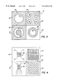
- FIG. 1 is a schematic of a photolithographic system.
- FIG. 2 is a schematic illustrating an embodiment of the present invention.
- FIG. 3 is a plan view of an optical element.
- FIG. 4 is a plan view of a reticle.
- FIG. 1 schematically illustrates a photolithographic system 10 .
- Illumination source 12 projects electromagnetic radiation through an optical element 14 and onto a reticle 16 .
- An illumination plane is formed at the reticle 16 .
- An image of the reticle 16 is projected onto a wafer 20 by projection optics 18 .
- Wafer 20 has a photosensitive resist coating thereon which is exposed by the image of the reticle 16 .
- Wafer 20 is mounted on a wafer stage 22 which is movable in the X and Y direction. In some photolithography operations, the wafer stage 22 may also be scanned along one axis.
- the illumination source 12 may be any illumination source or system, such as that disclosed in U.S. patent application Ser. No. 08/449,301 filed May 24, 1995 and entitled “Hybrid Illumination System For Use In Photolithography” by Stanton et al and issued May 20, 1997 as U.S. Pat. No. 5,631,721, which is herein incorporated by reference.
- FIG. 2 illustrates an illumination profile 24 created by the illumination source 12 , illustrated in FIG. 1 .
- the intensity profile 24 is relatively uniform.
- This relatively uniform illumination intensity profile 24 is projected through the optical element 14 .
- the optical element 14 then creates an illumination field or plane at or adjacent to the reticle 16 .
- the illumination plane formed at reticle 16 projects the image of the reticle 16 onto a photosensitive resist covered wafer 20 , illustrated in FIG. 1 .
- Electromagnetic radiation represented by lines 15 illustrate the different illumination properties, such as numerical aperture, fill geometry and others, provided over a region of the reticle by the optical element 14 .
- Electromagnetic radiation represented by lines 17 illustrate other, different illumination properties than those represented by lines 15 . While only several different illumination properties are illustrated, clearly there can be many different illumination properties spatially distributed over the reticle 16 by the optical element 14 . The number of different illumination regions depends on the reticle 14 and the degree of matching desired.
- FIG. 3 generally illustrates an optical element 14 as illustrated in FIGS. 1 and 2.
- the optical element 14 has several illumination regions 26 , 28 , 30 , and 32 thereon. These illumination regions 26 , 28 , 30 , and 32 may be formed by filters, diffractive optical elements, or preferably by a microlens arrays. Each of the plurality of different illumination regions, 26 , 28 , 30 , and 32 are used to control the illumination properties, such as for example numerical aperture, coherence, fill, and sag, of the resulting illumination used to project the image of the reticle 16 onto a photosensitive resist covered wafer 20 , illustrated in FIGS. 1 and 2.
- the illumination properties such as for example numerical aperture, coherence, fill, and sag
- illumination region 26 illustrates a quadrupole.
- a quadrupole illumination is characterized by several circular bright portions 36 located off-axis and surrounded by darker portions 34 .
- Quadrupole illumination may be achieved with pyramidal lenslets formed in a microlens array.
- Illumination region 28 illustrates an annular illumination region having a bright portion 38 surrounding a dark portion annular ring 40 surrounding a bright circular portion 39 .
- Illumination region 30 has a dark portion 42 surrounded by a bright annular portion 44 with a central dark portion 46 .
- the annular illumination patterns illustrated in illumination regions 30 and 28 may be formed by conical lenslets in a microlens array.
- Illumination region 32 is formed by a dark portion 48 surrounding a bright circular portion 50 forming a top hat.
- the illumination pattern illustrated in top hat region 32 may be formed by hexagonal close packed parabolic lenslets in a microlens array.
- the illumination regions 26 , 28 , 30 , and 32 graphically illustrate several different illumination properties that may be desired. These different illumination properties may include a desired pupil fill or angular distribution of electromagnetic radiation which may be in the form indicated above, namely, top hat illumination, annular illumination, or quadruple illumination.
- the actual optical elements used to produce the illumination properties graphically illustrated in FIG. 3 may physically appear quite different.
- FIG. 4 is a plan view illustrating a reticle having a plurality of different pattern regions 52 , 54 , 56 , and 58 .
- Each of the different pattern regions 52 , 54 , 56 , and 58 have a different geometrical pattern thereon.
- pattern region 52 has a right angle grid pattern 60 formed thereon.
- Pattern region 54 has an angled pattern 62 thereon.
- Pattern region 56 has a mixed right angle and angled pattern 64 thereon.
- Pattern region 58 has curved patterns thereon.
- the differing patterns illustrated at pattern regions 60 , 62 , 64 , and 68 are only by way of example, and illustrate that different patterns or geometric configurations are often present on a single reticle 16 that may be divided into different regions. Many other different patterns or geometric configurations may be used.
- the geometric configurations graphically illustrate different patterns. The actual patterns illustrated in FIG. 4 may physically appear quite different.
- Each illumination region 26 , 28 , 30 , and 32 formed by the optical element 14 produces an illumination profile having coherence and fill geometries that are matched to provide an optimized image considering the corresponding pattern regions 52 , 54 , 56 , and 58 on the reticle 16 .
- the illumination regions 26 , 28 , 30 , and 32 spatially correspond to the pattern regions 52 , 54 , 56 , and 58 . Accordingly, a more uniform image is obtained irrespective of the different pattern geometries found on a single reticle.
- illumination properties such as coherence may be varied spatially at different points to compensate for any deviation from desired performance of the illumination field or plane.
- illumination properties may be varied along one axis to compensate for certain imperfections in projection optics in a scanning type photolithographic tool where a rectangular illumination field is scanned across the reticle. This may be particularly advantageous in that illumination properties may be varied in a longitudinal direction of the rectangular slit being scanned, thereby compensating for any imperfections that may exist in the projection optics.
- optical elements having different illumination regions may not only be used to compensate for differing geometry on the reticle, but the different illumination regions may be used to compensate for imperfections in other optical elements, such as the projection optics, to improve exposure of a photosensitive resist covered wafer or substrate.
- the present invention has many practical applications in that different illumination regions can be created on a single optical element used to optimize the exposure of a photosensitive resist covered wafer, greatly augmenting overall system performance.
Abstract
Description
Claims (10)
Priority Applications (9)
| Application Number | Priority Date | Filing Date | Title |
|---|---|---|---|
| US08/799,107 US6259513B1 (en) | 1996-11-25 | 1997-02-11 | Illumination system with spatially controllable partial coherence |
| DE69739228T DE69739228D1 (en) | 1996-11-25 | 1997-10-30 | Lighting system with adjustable partial coherence |
| EP97118963A EP0844529B1 (en) | 1996-11-25 | 1997-10-30 | Illumination system with spatially controllable partial coherence |
| KR1019970062663A KR100517215B1 (en) | 1996-11-25 | 1997-11-25 | Optical element, imaging system and photolithography tool with spatially controllable partial coherence |
| JP32318097A JP4222650B2 (en) | 1996-11-25 | 1997-11-25 | Optical element |
| CA002222110A CA2222110A1 (en) | 1996-11-25 | 1997-11-25 | Illumination system with spatially controllable partial coherence |
| US09/599,383 US6628370B1 (en) | 1996-11-25 | 2000-06-22 | Illumination system with spatially controllable partial coherence compensating for line width variances in a photolithographic system |
| US10/667,387 US6822728B2 (en) | 1996-11-25 | 2003-09-23 | Illumination system with spatially controllable partial coherence compensation for line width variances in a photolithographic system |
| US10/961,200 US7092070B2 (en) | 1996-11-25 | 2004-10-12 | Illumination system with spatially controllable partial coherence compensating for line width variances |
Applications Claiming Priority (2)
| Application Number | Priority Date | Filing Date | Title |
|---|---|---|---|
| US3172596P | 1996-11-25 | 1996-11-25 | |
| US08/799,107 US6259513B1 (en) | 1996-11-25 | 1997-02-11 | Illumination system with spatially controllable partial coherence |
Related Child Applications (1)
| Application Number | Title | Priority Date | Filing Date |
|---|---|---|---|
| US09/599,383 Continuation-In-Part US6628370B1 (en) | 1996-11-25 | 2000-06-22 | Illumination system with spatially controllable partial coherence compensating for line width variances in a photolithographic system |
Publications (1)
| Publication Number | Publication Date |
|---|---|
| US6259513B1 true US6259513B1 (en) | 2001-07-10 |
Family
ID=26707543
Family Applications (1)
| Application Number | Title | Priority Date | Filing Date |
|---|---|---|---|
| US08/799,107 Expired - Fee Related US6259513B1 (en) | 1996-11-25 | 1997-02-11 | Illumination system with spatially controllable partial coherence |
Country Status (6)
| Country | Link |
|---|---|
| US (1) | US6259513B1 (en) |
| EP (1) | EP0844529B1 (en) |
| JP (1) | JP4222650B2 (en) |
| KR (1) | KR100517215B1 (en) |
| CA (1) | CA2222110A1 (en) |
| DE (1) | DE69739228D1 (en) |
Cited By (19)
| Publication number | Priority date | Publication date | Assignee | Title |
|---|---|---|---|---|
| US20020187435A1 (en) * | 2001-04-03 | 2002-12-12 | Stmicroelectronics S.A. | Method of illuminating a layer of a material, in particular of photosensitive resin |
| US20020196629A1 (en) * | 2001-05-31 | 2002-12-26 | Takaaki Terashi | Illumination apparatus, illumination-controlling method, exposure apparatus, device fabricating method |
| US20030044693A1 (en) * | 2001-08-30 | 2003-03-06 | Boettiger Ulrich C. | Method and apparatus for irradiating a microlithographic substrate |
| US6563567B1 (en) | 1998-12-17 | 2003-05-13 | Nikon Corporation | Method and apparatus for illuminating a surface using a projection imaging apparatus |
| US6628370B1 (en) * | 1996-11-25 | 2003-09-30 | Mccullough Andrew W. | Illumination system with spatially controllable partial coherence compensating for line width variances in a photolithographic system |
| US20030197846A1 (en) * | 2002-04-23 | 2003-10-23 | Asml Us, Inc. | System and method for improving line width control in a lithography device using an illumination system having pre-numerical aperture control |
| US20030214643A1 (en) * | 1999-12-13 | 2003-11-20 | Asml Netherlands B.V. | Illuminator for a lithography apparatus, a lithography apparatus comprising such an illuminator, and a manufacturing method employing such a lithography apparatus |
| US6794100B2 (en) | 2001-08-30 | 2004-09-21 | Micron Technology, Inc. | Method for controlling radiation beam intensity directed to microlithographic substrates |
| US20050078293A1 (en) * | 2003-10-14 | 2005-04-14 | Mackey Jeffrey L. | Methods and systems for controlling radiation beam characteristics for microlithographic processing |
| US6888615B2 (en) * | 2002-04-23 | 2005-05-03 | Asml Holding N.V. | System and method for improving linewidth control in a lithography device by varying the angular distribution of light in an illuminator as a function of field position |
| US20050099614A1 (en) * | 1998-06-30 | 2005-05-12 | Canon Kabushiki Kaisha | Multiple exposure method |
| US20050264784A1 (en) * | 2004-05-26 | 2005-12-01 | Asml Netherlands B.V. | Lithographic apparatus and device manufacturing method |
| US20070019178A1 (en) * | 2005-07-25 | 2007-01-25 | Micron Technology, Inc. | Methods and apparatuses for configuring radiation in microlithographic processing of workpieces |
| US20070024836A1 (en) * | 2004-02-07 | 2007-02-01 | Carl Zeiss Smt Ag | Illumination system for a microlithographic projection exposure apparatus |
| US20070105029A1 (en) * | 2003-12-19 | 2007-05-10 | International Business Machines Corporation | Differential critical dimension and overlay metrology apparatus and measurement method |
| US20070109520A1 (en) * | 2005-11-17 | 2007-05-17 | Whitney Theodore R | Modular illuminator for a scanning printer |
| US20080259304A1 (en) * | 2007-04-20 | 2008-10-23 | Asml Netherlands B.V. | Lithographic apparatus and method |
| US20090047583A1 (en) * | 2007-08-13 | 2009-02-19 | Micron Technology, Inc. | Masks for microlithography and methods of making and using such masks |
| US9933704B2 (en) | 2010-06-15 | 2018-04-03 | Carl Zeiss Smt Gmbh | Microlithography illumination optical system and microlithography projection exposure apparatus including same |
Families Citing this family (9)
| Publication number | Priority date | Publication date | Assignee | Title |
|---|---|---|---|---|
| JP2001174615A (en) * | 1999-04-15 | 2001-06-29 | Nikon Corp | Diffraction optical element, method of producing the element, illumination device equipped with the element, projection exposure device, exposure method, light homogenizer, and method of producing the light homogenizer |
| US6563566B2 (en) * | 2001-01-29 | 2003-05-13 | International Business Machines Corporation | System and method for printing semiconductor patterns using an optimized illumination and reticle |
| TWI285295B (en) * | 2001-02-23 | 2007-08-11 | Asml Netherlands Bv | Illumination optimization in lithography |
| US6573975B2 (en) | 2001-04-04 | 2003-06-03 | Pradeep K. Govil | DUV scanner linewidth control by mask error factor compensation |
| JP4305611B2 (en) * | 2002-07-18 | 2009-07-29 | 株式会社ニコン | Illumination optical apparatus, exposure apparatus, and exposure method |
| US6963434B1 (en) | 2004-04-30 | 2005-11-08 | Asml Holding N.V. | System and method for calculating aerial image of a spatial light modulator |
| KR100699111B1 (en) * | 2005-06-09 | 2007-03-22 | 동부일렉트로닉스 주식회사 | A light transmittance setting device for exposure |
| JP2007299993A (en) * | 2006-05-01 | 2007-11-15 | Canon Inc | Aligner |
| JP4971932B2 (en) | 2007-10-01 | 2012-07-11 | キヤノン株式会社 | Illumination optical system, exposure apparatus, device manufacturing method, and polarization control unit |
Citations (17)
| Publication number | Priority date | Publication date | Assignee | Title |
|---|---|---|---|---|
| US4621922A (en) * | 1983-08-12 | 1986-11-11 | Perkin-Elmer Censor Anstalt | Device for the projection copying of masks onto a workpiece |
| EP0486316A2 (en) | 1990-11-15 | 1992-05-20 | Nikon Corporation | Projection exposure method and apparatus |
| US5184176A (en) * | 1990-10-08 | 1993-02-02 | Canon Kabushiki Kaisha | Projection exposure apparatus with an aberration compensation device of a projection lens |
| EP0564264A1 (en) | 1992-03-31 | 1993-10-06 | Canon Kabushiki Kaisha | Illumination device for projection exposure apparatus |
| US5296892A (en) | 1992-02-01 | 1994-03-22 | Nikon Corporation | Illuminating apparatus and projection exposure apparatus provided with such an illuminating apparatus |
| US5329336A (en) * | 1992-07-06 | 1994-07-12 | Nikon Corporation | Exposure method and apparatus |
| US5357312A (en) | 1992-10-01 | 1994-10-18 | Nec Corporation | Illuminating system in exposure apparatus for photolithography |
| US5383000A (en) | 1992-11-24 | 1995-01-17 | General Signal Corporation | Partial coherence varier for microlithographic system |
| JPH0794399A (en) | 1993-09-24 | 1995-04-07 | Toshiba Corp | Method and device for exposure |
| JPH07201723A (en) | 1993-12-28 | 1995-08-04 | Toshiba Corp | Aligning method and device |
| US5446587A (en) * | 1992-09-03 | 1995-08-29 | Samsung Electronics Co., Ltd. | Projection method and projection system and mask therefor |
| US5631721A (en) * | 1995-05-24 | 1997-05-20 | Svg Lithography Systems, Inc. | Hybrid illumination system for use in photolithography |
| US5642183A (en) * | 1993-08-27 | 1997-06-24 | Sharp Kabushiki Kaisha | Spatial filter used in a reduction-type projection printing apparatus |
| US5673103A (en) | 1993-09-24 | 1997-09-30 | Kabushiki Kaisha Toshiba | Exposure apparatus and method |
| US5684566A (en) * | 1995-05-24 | 1997-11-04 | Svg Lithography Systems, Inc. | Illumination system and method employing a deformable mirror and diffractive optical elements |
| US6049374A (en) * | 1997-03-14 | 2000-04-11 | Nikon Corporation | Illumination apparatus, a projection exposure apparatus having the same, a method of manufacturing a device using the same, and a method of manufacturing the projection exposure apparatus |
| US6078380A (en) * | 1991-10-08 | 2000-06-20 | Nikon Corporation | Projection exposure apparatus and method involving variation and correction of light intensity distributions, detection and control of imaging characteristics, and control of exposure |
-
1997
- 1997-02-11 US US08/799,107 patent/US6259513B1/en not_active Expired - Fee Related
- 1997-10-30 EP EP97118963A patent/EP0844529B1/en not_active Expired - Lifetime
- 1997-10-30 DE DE69739228T patent/DE69739228D1/en not_active Expired - Fee Related
- 1997-11-25 CA CA002222110A patent/CA2222110A1/en not_active Abandoned
- 1997-11-25 JP JP32318097A patent/JP4222650B2/en not_active Expired - Fee Related
- 1997-11-25 KR KR1019970062663A patent/KR100517215B1/en not_active IP Right Cessation
Patent Citations (17)
| Publication number | Priority date | Publication date | Assignee | Title |
|---|---|---|---|---|
| US4621922A (en) * | 1983-08-12 | 1986-11-11 | Perkin-Elmer Censor Anstalt | Device for the projection copying of masks onto a workpiece |
| US5184176A (en) * | 1990-10-08 | 1993-02-02 | Canon Kabushiki Kaisha | Projection exposure apparatus with an aberration compensation device of a projection lens |
| EP0486316A2 (en) | 1990-11-15 | 1992-05-20 | Nikon Corporation | Projection exposure method and apparatus |
| US6078380A (en) * | 1991-10-08 | 2000-06-20 | Nikon Corporation | Projection exposure apparatus and method involving variation and correction of light intensity distributions, detection and control of imaging characteristics, and control of exposure |
| US5296892A (en) | 1992-02-01 | 1994-03-22 | Nikon Corporation | Illuminating apparatus and projection exposure apparatus provided with such an illuminating apparatus |
| EP0564264A1 (en) | 1992-03-31 | 1993-10-06 | Canon Kabushiki Kaisha | Illumination device for projection exposure apparatus |
| US5329336A (en) * | 1992-07-06 | 1994-07-12 | Nikon Corporation | Exposure method and apparatus |
| US5446587A (en) * | 1992-09-03 | 1995-08-29 | Samsung Electronics Co., Ltd. | Projection method and projection system and mask therefor |
| US5357312A (en) | 1992-10-01 | 1994-10-18 | Nec Corporation | Illuminating system in exposure apparatus for photolithography |
| US5383000A (en) | 1992-11-24 | 1995-01-17 | General Signal Corporation | Partial coherence varier for microlithographic system |
| US5642183A (en) * | 1993-08-27 | 1997-06-24 | Sharp Kabushiki Kaisha | Spatial filter used in a reduction-type projection printing apparatus |
| US5673103A (en) | 1993-09-24 | 1997-09-30 | Kabushiki Kaisha Toshiba | Exposure apparatus and method |
| JPH0794399A (en) | 1993-09-24 | 1995-04-07 | Toshiba Corp | Method and device for exposure |
| JPH07201723A (en) | 1993-12-28 | 1995-08-04 | Toshiba Corp | Aligning method and device |
| US5631721A (en) * | 1995-05-24 | 1997-05-20 | Svg Lithography Systems, Inc. | Hybrid illumination system for use in photolithography |
| US5684566A (en) * | 1995-05-24 | 1997-11-04 | Svg Lithography Systems, Inc. | Illumination system and method employing a deformable mirror and diffractive optical elements |
| US6049374A (en) * | 1997-03-14 | 2000-04-11 | Nikon Corporation | Illumination apparatus, a projection exposure apparatus having the same, a method of manufacturing a device using the same, and a method of manufacturing the projection exposure apparatus |
Cited By (57)
| Publication number | Priority date | Publication date | Assignee | Title |
|---|---|---|---|---|
| US20040057033A1 (en) * | 1996-11-25 | 2004-03-25 | Mccullough Andrew W. | Illumination system with spatially controllable partial coherence compensation for line width variances in a photolithographic system |
| US20050041231A1 (en) * | 1996-11-25 | 2005-02-24 | Asml Holding N.V. | Illumination system with spatially controllable partial coherence compensating for line width variances |
| US6822728B2 (en) | 1996-11-25 | 2004-11-23 | Asml Holding N.V. | Illumination system with spatially controllable partial coherence compensation for line width variances in a photolithographic system |
| US6628370B1 (en) * | 1996-11-25 | 2003-09-30 | Mccullough Andrew W. | Illumination system with spatially controllable partial coherence compensating for line width variances in a photolithographic system |
| US7092070B2 (en) | 1996-11-25 | 2006-08-15 | Asml Holding N.V. | Illumination system with spatially controllable partial coherence compensating for line width variances |
| US6930754B1 (en) * | 1998-06-30 | 2005-08-16 | Canon Kabushiki Kaisha | Multiple exposure method |
| US7505112B2 (en) | 1998-06-30 | 2009-03-17 | Canon Kabushiki Kaisha | Multiple exposure method |
| US20050099614A1 (en) * | 1998-06-30 | 2005-05-12 | Canon Kabushiki Kaisha | Multiple exposure method |
| US7023522B2 (en) | 1998-06-30 | 2006-04-04 | Canon Kabushiki Kaisha | Multiple exposure method |
| US20080198350A1 (en) * | 1998-06-30 | 2008-08-21 | Canon Kabushiki Kaisha | Multiple exposure method |
| US20030156269A1 (en) * | 1998-12-17 | 2003-08-21 | Nikon Corporation | Method and apparatus for illuminating a surface using a projection imaging apparatus |
| US20030160949A1 (en) * | 1998-12-17 | 2003-08-28 | Nikon Corporation | Method and apparatus for illuminating a surface using a projection imaging apparatus |
| US20030156266A1 (en) * | 1998-12-17 | 2003-08-21 | Nikon Corporation | Method and apparatus for illuminating a surface using a projection imaging apparatus |
| US6563567B1 (en) | 1998-12-17 | 2003-05-13 | Nikon Corporation | Method and apparatus for illuminating a surface using a projection imaging apparatus |
| US20030214643A1 (en) * | 1999-12-13 | 2003-11-20 | Asml Netherlands B.V. | Illuminator for a lithography apparatus, a lithography apparatus comprising such an illuminator, and a manufacturing method employing such a lithography apparatus |
| US6833907B2 (en) * | 1999-12-13 | 2004-12-21 | Asml Netherlands B.V. | Illuminator for a lithography apparatus, a lithography apparatus comprising such an illuminator, and a manufacturing method employing such a lithography apparatus |
| US20020187435A1 (en) * | 2001-04-03 | 2002-12-12 | Stmicroelectronics S.A. | Method of illuminating a layer of a material, in particular of photosensitive resin |
| US6934009B2 (en) | 2001-05-31 | 2005-08-23 | Canon Kabushiki Kaisha | Illumination apparatus, illumination-controlling method, exposure apparatus, device fabricating method |
| US20020196629A1 (en) * | 2001-05-31 | 2002-12-26 | Takaaki Terashi | Illumination apparatus, illumination-controlling method, exposure apparatus, device fabricating method |
| US7038762B2 (en) | 2001-08-30 | 2006-05-02 | Micron Technology, Inc. | Method and apparatus for irradiating a microlithographic substrate |
| US20060158631A1 (en) * | 2001-08-30 | 2006-07-20 | Micron Technology, Inc. | Method and apparatus for irradiating a microlithographic substrate |
| US20030044693A1 (en) * | 2001-08-30 | 2003-03-06 | Boettiger Ulrich C. | Method and apparatus for irradiating a microlithographic substrate |
| US7298453B2 (en) | 2001-08-30 | 2007-11-20 | Micron Technology, Inc. | Method and apparatus for irradiating a microlithographic substrate |
| US20050041228A1 (en) * | 2001-08-30 | 2005-02-24 | Boettiger Ulrich C. | Method and apparatus for irradiating a microlithographic substrate |
| US20040234871A1 (en) * | 2001-08-30 | 2004-11-25 | Boettiger Ulrich C. | Method and apparatus for controlling radiation beam intensity directed to microlithographic substrates |
| US7230679B2 (en) | 2001-08-30 | 2007-06-12 | Micron Technology, Inc. | Method and apparatus for controlling radiation beam intensity directed to microlithographic substrates |
| US20060181692A1 (en) * | 2001-08-30 | 2006-08-17 | Micron Technology, Inc. | Method and apparatus for controlling radiation beam intensity directed to microlithograhic substrates |
| US6794100B2 (en) | 2001-08-30 | 2004-09-21 | Micron Technology, Inc. | Method for controlling radiation beam intensity directed to microlithographic substrates |
| US6784975B2 (en) | 2001-08-30 | 2004-08-31 | Micron Technology, Inc. | Method and apparatus for irradiating a microlithographic substrate |
| US7046340B2 (en) | 2001-08-30 | 2006-05-16 | Micron Technology, Inc. | Method and apparatus for controlling radiation beam intensity directed to microlithographic substrates |
| CN1307485C (en) * | 2002-04-23 | 2007-03-28 | Asml美国公司 | System and method for improving line width control in use of photoetching apparatus of illuminating system with prenumerical value aperture control |
| US20030197846A1 (en) * | 2002-04-23 | 2003-10-23 | Asml Us, Inc. | System and method for improving line width control in a lithography device using an illumination system having pre-numerical aperture control |
| US6784976B2 (en) * | 2002-04-23 | 2004-08-31 | Asml Holding N.V. | System and method for improving line width control in a lithography device using an illumination system having pre-numerical aperture control |
| US6888615B2 (en) * | 2002-04-23 | 2005-05-03 | Asml Holding N.V. | System and method for improving linewidth control in a lithography device by varying the angular distribution of light in an illuminator as a function of field position |
| US20060176462A1 (en) * | 2003-10-14 | 2006-08-10 | Micron Technology, Inc. | Methods and systems for controlling radiation beam characteristics for microlithographic processing |
| US7130022B2 (en) | 2003-10-14 | 2006-10-31 | Micron Technology, Inc. | Methods and systems for controlling radiation beam characteristics for microlithographic processing |
| US7053987B2 (en) | 2003-10-14 | 2006-05-30 | Micron Technology, Inc. | Methods and systems for controlling radiation beam characteristics for microlithographic processing |
| US20050078293A1 (en) * | 2003-10-14 | 2005-04-14 | Mackey Jeffrey L. | Methods and systems for controlling radiation beam characteristics for microlithographic processing |
| US20050200824A1 (en) * | 2003-10-14 | 2005-09-15 | Micron Technology, Inc. | Methods and systems for controlling radiation beam characteristics for microlithographic processing |
| US6894765B2 (en) | 2003-10-14 | 2005-05-17 | Micron Technology, Inc. | Methods and systems for controlling radiation beam characteristics for microlithographic processing |
| US8035824B2 (en) | 2003-12-19 | 2011-10-11 | International Business Machines Corporation | Differential critical dimension and overlay metrology apparatus and measurement method |
| US7700247B2 (en) | 2003-12-19 | 2010-04-20 | International Business Machines Corporation | Differential critical dimension and overlay metrology apparatus and measurement method |
| US20070105029A1 (en) * | 2003-12-19 | 2007-05-10 | International Business Machines Corporation | Differential critical dimension and overlay metrology apparatus and measurement method |
| US20070024836A1 (en) * | 2004-02-07 | 2007-02-01 | Carl Zeiss Smt Ag | Illumination system for a microlithographic projection exposure apparatus |
| US7400381B2 (en) * | 2004-05-26 | 2008-07-15 | Asml Netherlands B.V. | Lithographic apparatus and device manufacturing method |
| US20050264784A1 (en) * | 2004-05-26 | 2005-12-01 | Asml Netherlands B.V. | Lithographic apparatus and device manufacturing method |
| US20070019178A1 (en) * | 2005-07-25 | 2007-01-25 | Micron Technology, Inc. | Methods and apparatuses for configuring radiation in microlithographic processing of workpieces |
| US20090040494A1 (en) * | 2005-07-25 | 2009-02-12 | Micron Technology, Inc. | Methods and apparatuses for configuring radiation in microlithographic processing of workpieces |
| US7446855B2 (en) | 2005-07-25 | 2008-11-04 | Micron Technology, Inc | Methods and apparatuses for configuring radiation in microlithographic processing of workpieces using an adjustment structure |
| US20070109520A1 (en) * | 2005-11-17 | 2007-05-17 | Whitney Theodore R | Modular illuminator for a scanning printer |
| US20080259304A1 (en) * | 2007-04-20 | 2008-10-23 | Asml Netherlands B.V. | Lithographic apparatus and method |
| US20090047583A1 (en) * | 2007-08-13 | 2009-02-19 | Micron Technology, Inc. | Masks for microlithography and methods of making and using such masks |
| US7838178B2 (en) | 2007-08-13 | 2010-11-23 | Micron Technology, Inc. | Masks for microlithography and methods of making and using such masks |
| US20110045388A1 (en) * | 2007-08-13 | 2011-02-24 | Micron Technology, Inc. | Masks for microlithography and methods of making and using such masks |
| US7972753B2 (en) | 2007-08-13 | 2011-07-05 | Micron Technology, Inc. | Masks for microlithography and methods of making and using such masks |
| US8859168B2 (en) | 2007-08-13 | 2014-10-14 | Micron Technology, Inc. | Masks for microlithography and methods of making and using such masks |
| US9933704B2 (en) | 2010-06-15 | 2018-04-03 | Carl Zeiss Smt Gmbh | Microlithography illumination optical system and microlithography projection exposure apparatus including same |
Also Published As
| Publication number | Publication date |
|---|---|
| EP0844529B1 (en) | 2009-01-21 |
| EP0844529A3 (en) | 2000-01-05 |
| DE69739228D1 (en) | 2009-03-12 |
| CA2222110A1 (en) | 1998-05-25 |
| EP0844529A2 (en) | 1998-05-27 |
| KR100517215B1 (en) | 2005-12-06 |
| JPH10233362A (en) | 1998-09-02 |
| KR19980042721A (en) | 1998-08-17 |
| JP4222650B2 (en) | 2009-02-12 |
Similar Documents
| Publication | Publication Date | Title |
|---|---|---|
| US6259513B1 (en) | Illumination system with spatially controllable partial coherence | |
| US7092070B2 (en) | Illumination system with spatially controllable partial coherence compensating for line width variances | |
| JP4169374B2 (en) | Illumination means for projection microlithography apparatus | |
| JPH1154426A (en) | Lighting device and aligner using the same | |
| JP2001174615A (en) | Diffraction optical element, method of producing the element, illumination device equipped with the element, projection exposure device, exposure method, light homogenizer, and method of producing the light homogenizer | |
| JPS60232552A (en) | Lighting optical system | |
| JPS60218635A (en) | Lighting device | |
| JP3165711B2 (en) | Image projection method and method for manufacturing semiconductor device using the method | |
| USRE34634E (en) | Light illumination device | |
| KR100823405B1 (en) | Exposure apparatus and device manufacturing method | |
| JPH09219358A (en) | Aligner, and device manufacturing method using the same | |
| US5300967A (en) | Projection exposure apparatus | |
| KR100773995B1 (en) | Device and method for improving line width control in a lithography device using an illumination system having pre-numerical aperture control | |
| KR100733547B1 (en) | System and method for improving linewidth control in a lithography device by varying the angular distribution of light in an illuminator as a function of field position | |
| US5386266A (en) | Projection exposure system | |
| JP2914035B2 (en) | Ring light flux forming method and illumination optical device | |
| JPH07201697A (en) | Aligner | |
| JP3376043B2 (en) | Illumination device and projection exposure apparatus using the same | |
| KR100496078B1 (en) | Lighting system used in scanning lithography | |
| JP2947038B2 (en) | Reduction projection exposure equipment | |
| JP3077307B2 (en) | Lighting equipment for exposure | |
| JPH0594936A (en) | Ring band lighting system |
Legal Events
| Date | Code | Title | Description |
|---|---|---|---|
| AS | Assignment |
Owner name: SVG LITHOGRAPHY SYSTEMS, INC., CONNECTICUT Free format text: ASSIGNMENT OF ASSIGNORS INTEREST;ASSIGNORS:GALLATIN, GREGG;MCCULLOUGH, ANDREW W.;REEL/FRAME:008501/0572 Effective date: 19970204 |
|
| FEPP | Fee payment procedure |
Free format text: PAYOR NUMBER ASSIGNED (ORIGINAL EVENT CODE: ASPN); ENTITY STATUS OF PATENT OWNER: LARGE ENTITY |
|
| AS | Assignment |
Owner name: ASML HOLDING N.V., NETHERLANDS Free format text: CERTIFICATE OF OWNERSHIP AND MERGER, CONVERSION, MERGER, AND CONFIRMATORY ASSIGNMENT;ASSIGNORS:SVG LITHOGRAPHY SYSTEMS, INC.;ASML US, INC.;ASM LITHOGRAPHY, INC. AND ASML US, LLC;AND OTHERS;REEL/FRAME:014484/0588;SIGNING DATES FROM 20011231 TO 20031009 Owner name: ASML US, INC., ARIZONA Free format text: CERTIFICATE OF OWNERSHIP AND MERGER, CONVERSION, MERGER, AND CONFIRMATORY ASSIGNMENT;ASSIGNORS:SVG LITHOGRAPHY SYSTEMS, INC.;ASML US, INC.;ASM LITHOGRAPHY, INC. AND ASML US, LLC;AND OTHERS;REEL/FRAME:014484/0588;SIGNING DATES FROM 20011231 TO 20031009 Owner name: ASML US, LLC, DELAWARE Free format text: CERTIFICATE OF OWNERSHIP AND MERGER, CONVERSION, MERGER, AND CONFIRMATORY ASSIGNMENT;ASSIGNORS:SVG LITHOGRAPHY SYSTEMS, INC.;ASML US, INC.;ASM LITHOGRAPHY, INC. AND ASML US, LLC;AND OTHERS;REEL/FRAME:014484/0588;SIGNING DATES FROM 20011231 TO 20031009 |
|
| FPAY | Fee payment |
Year of fee payment: 4 |
|
| FPAY | Fee payment |
Year of fee payment: 8 |
|
| REMI | Maintenance fee reminder mailed | ||
| LAPS | Lapse for failure to pay maintenance fees | ||
| STCH | Information on status: patent discontinuation |
Free format text: PATENT EXPIRED DUE TO NONPAYMENT OF MAINTENANCE FEES UNDER 37 CFR 1.362 |
|
| FP | Lapsed due to failure to pay maintenance fee |
Effective date: 20130710 |