US6249798B1 - Method, apparatus and computer system for directly transferring and translating data between an integer processing unit and a floating point processing unit - Google Patents
Method, apparatus and computer system for directly transferring and translating data between an integer processing unit and a floating point processing unit Download PDFInfo
- Publication number
- US6249798B1 US6249798B1 US08/728,646 US72864696A US6249798B1 US 6249798 B1 US6249798 B1 US 6249798B1 US 72864696 A US72864696 A US 72864696A US 6249798 B1 US6249798 B1 US 6249798B1
- Authority
- US
- United States
- Prior art keywords
- floating point
- format
- data
- register
- integer
- Prior art date
- Legal status (The legal status is an assumption and is not a legal conclusion. Google has not performed a legal analysis and makes no representation as to the accuracy of the status listed.)
- Expired - Lifetime
Links
Images


Classifications
-
- H—ELECTRICITY
- H03—ELECTRONIC CIRCUITRY
- H03M—CODING; DECODING; CODE CONVERSION IN GENERAL
- H03M7/00—Conversion of a code where information is represented by a given sequence or number of digits to a code where the same, similar or subset of information is represented by a different sequence or number of digits
- H03M7/14—Conversion to or from non-weighted codes
- H03M7/24—Conversion to or from floating-point codes
Definitions
- the present invention relates to a transfer and translation of information between an integer processing unit and a floating point processing unit. More particularly, the present invention relates to direct transfer between and translation of data stored in a memory format in integer registers of the integer processing unit and data stored in a floating point format in floating point registers of the floating point processing unit.
- integer and floating point processing units within or in conjunction with a microprocessor is well known in the data processing art.
- the integer processing unit provides the basic arithmetic and logical operations for the processor when the information is in integer format and the floating point processing unit provides the basic arithmetic and logical operations for the processor in floating point format when floating point operations are to be performed.
- there are two sets of registers including a first set of integer registers for the integer unit and a second set of floating point registers for the floating point unit.
- the bit length of the two register sets may differ in order to accommodate the higher precision capability of the floating point unit.
- the integer registers may each be 32 bits in length, while the floating point registers may each be 64 bits or greater.
- a typical integer unit includes a number of integer registers which store information and one or more integer execution units which operate on the stored information based on instructions conveyed to the execution unit(s).
- the integer registers for the integer unit are sometimes collectively referred to as a file (e.g., a register file, an integer register file or an integer file).
- the integer register files are also coupled to a bus for transfer of information to other units, such as memory.
- information can be loaded from memory to the integer register file, operated on by one or more integer execution unit (which calculation is returned to the register file) and the result ultimately stored back in the memory.
- the floating point processing unit is configured similarly to the integer processing unit in that it also includes a number of registers which load and store information from other units such as memory.
- the floating point processing unit includes one or more execution units which operate based on floating point instructions.
- Exponent operation Adding an integer value to an exponent of a floating point number to scale the number.
- Boolean operation Compounding Boolean values generated as a result of integer compares, as well as floating point compares.
- Inter-conversion operation Multiplying a floating point value with an integer value currently in the integer register file, which will require the movement of the integer value to the floating point register file and converting or translating it into floating point format.
- single precision calculations have been performed on a single precision data format, which has been defined as having a bit length of 32 bits.
- the single precision data format includes 23 significand bits, 8 exponent bits and one sign bit.
- a double precision data format has previously been implemented using a bit length of 64 bits.
- the double precision data format includes 52 significand bits, 11 exponent bits and one sign bit.
- Floating point operations have typicallly been performed on data in the double precision data format. Accordingly, integer register files have included integer registers of 32 bits in length, while floating point register files have included registers of 64 bits in length.
- the manipulation of single and double precision formats was simplified by the fact that the double precision format was exactly twice the length of the single precision format.
- microprocessors have extended the floating point capability to more than double precision.
- One microprocessor family developed by Intel Corporation e.g., the 80386, 80486 and PentiumTM microprocessors
- the extended precision is an extension of the 64 bit double precision format and conforms to ANSI/IEEE (American National Standards Institute/The Institute of Electrical and Electronics Engineers) Standard 754 (1985), which is titled “IEEE Standard for Binary Floating-Point Arithmetic”.
- the extended precision format has been defined to have a bit length of 80 bits.
- the floating point data format might have a bit length of 80 bits to accommodate the extended precision format, it is possible for future floating point formats to have a larger number of bits (e.g., 82 or more bits).
- a current trend in microprocessor design is to extend the integer registers to have a bit length of 64 bits. Such a design requirement is prerequisite for microprocessors utilizing a 64-bit architecture (64 bits of addressing and data).
- integer units will utilize integer registers having 64 bits in length
- floating point units will utilize floating point registers having 80 bits or more bits in length (e.g., 82 bits in length).
- coupling of the integer register files of the integer processing unit and the floating point register files of the floating point processing units will involve transfers between 32 or 64 bit single or double precision memory format data values and 80 or 82 bit floating point format data values.
- the above-mentioned copending applications disclose techniques for providing coupling between integer and floating point units.
- the coupling arrangements of these applications are referred to as “moderately coupled”, since the arrangement provides more coupling than a fully decoupled scheme, but less coupling than a fully coupled scheme.
- the arrangements of these applications disclose advantageous “moderately coupled” arrangements between the integer unit and the floating point unit, they do not address any data format translation between the memory format in which data are stored in the integer unit and the floating point format in which data are stored in the floating point unit.
- the present invention provides for direct transfer and translation of data between memory format data in an integer processing unit and floating point data in a floating point processing unit.
- a direct data link is provided between integer registers of the integer processing unit and floating point registers of the floating point processing unit.
- a logic circuit is arranged in the direct data link which translates data between the memory format (or memory formats) used in the integer registers and the floating point format used in the floating point registers as it is transferred between the integer registers and the floating point registers.
- the present invention provides direct transfer and translation between memory format data stored in the integer registers and floating point data stored in the floating point registers.
- the present invention provides a data translation between memory format and floating point format without significant delays. That is, since the present invention provides a direct transfer and data translation between the integer processing unit and the floating point processing unit, data translation and transfer can be implemented quickly and economically.
- FIG. 1 illustrates an arrangement for direct data transfer and translation between an integer processing unit and a floating point processing unit according to an exemplary embodiment of the present invention.
- FIG. 2 illustrates data translation from floating point format data to single precision memory format data according to an exemplary embodiment of the present invention.
- FIG. 3 illustrates data translation from floating point format data to double precision memory format data according to an exemplary embodiment of the present invention.
- FIG. 4 illustrates data translation from single precision memory format data to floating point format data according to an exemplary embodiment of the present invention.
- FIG. 5 illustrates data translation from double precision memory format data to floating point format data according to an exemplary embodiment of the present invention.
- FIG. 6 illustrates data translation from floating point format data to single precision memory format data according to an exemplary embodiment of the present invention.
- FIG. 7 illustrates data translation from floating point format data to double precision memory format data according to an exemplary embodiment of the present invention.
- FIG. 8 illustrates data translation from single precision memory format data to floating point format data according to an exemplary embodiment of the present invention.
- FIG. 9 illustrates data translation from double precision memory format data to floating point format data according to an exemplary embodiment of the present invention.
- FIG. 10 illustrates an arrangement for direct data transfer and translation between an integer processing unit and a floating point processing unit according to a further exemplary embodiment of the present invention.
- FIG. 11 illustrates an arrangement for direct data transfer and translation between an integer processing unit and a floating point processing unit according to yet another exemplary embodiment of the present invention.
- a direct data link providing data transfer and translation between a floating point processing unit and integer processing unit which may be used in a processor is described herein.
- numerous specific details are set forth, such as specific registers, arithmetic and logic execution units, bit length formats for data words, etc., in order to provide a thorough understanding of the present invention.
- integer and floating point processing units for providing arithmetic and logical calculations is well known in the art. These units can be configured separately from a microprocessor to provide the arithmetic (or logical) operations on data. However, it is generally understood that “state-of-the-art” microprocessors will include both of these units as part of the microprocessor “chip”. Additionally, it is further understood that data stored in some form of memory will be accessed by one or both of these numeric units.
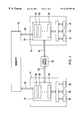
- FIG. 1 illustrates an arrangement for direct data transfer and translation between data in a memory format in an integer processing unit and data in a floating point format in a floating point processing unit according to an exemplary embodiment of the present invention.
- FIG. 1 includes a memory 12 , an integer processing unit 14 and a floating point processing unit 16 .
- the integer processing unit 14 includes an integer register file 18 , which is coupled to memory 12 by a bus 22 .
- the integer processing unit 14 is utilized to provide operations other than floating point operations.
- the floating point processing unit 16 is separate from the integer processing unit 14 and is utilized to provide all floating point operations.
- the floating point processing unit 16 includes a floating point register file 20 , which is also coupled to memory 12 by a bus 24 .
- buses 22 and 24 may actually be the same single bus coupling memory 12 to both integer processing unit 14 and floating point processing unit 16 .
- memory 12 of FIG. 1 can include multiple or different memories.
- memory 12 can include multiple or different memories.
- cache memory usually resident on the processor chip
- RAM random access memory
- non-volatile mass storage memory such as a magnetic storage media
- the single bus including bus 22 and bus 24 may actually be more than a single bus, such as in the instance where multiple bus levels are used to couple data to and from memory 12 if memory 12 is configured to be distant from the integer register files 18 and the floating point register files 20 .
- Both register files 18 and 20 each include a plurality of registers 26 and 28 , respectively. Although the actual number of such registers is a design choice, it is typical to have a number of registers equal to an exponential value of two. Accordingly, it is typical to have 32 or 64 such registers in each of the register files 18 and 20 . In the illustrated embodiment, there are 32 integer registers 26 in the integer register file 18 and 32 floating point registers 28 in the floating point register file 20 .
- bit-length of the registers is also a design choice dependent on the processor architecture.
- integer registers 26 of FIG. 1 are 64-bit registers in order to provide larger addressing capability. Since it is anticipated that addresses and data transfers to and from memory 12 will be accomplished utilizing a 64-bit architecture with the newer generations of microprocessors, the arrangement of FIG. 1 adapts to this newer convention.
- the floating point registers 28 of FIG. 1 are 82 bits in length in order to accommodate the floating point register format. Although the floating point registers are described herein as being 82 bits in length, the size (or bit length) of the floating point registers is a design choice and any floating point register bit length may be used in implementing the present invention.
- a plurality of integer execution units 32 , 34 and 36 are coupled to the integer register file 18 . Although only three integer execution units 32 , 34 and 36 are illustrated in FIG. 1, the actual number of integer execution units is a design choice. Likewise, a plurality of floating point execution units 42 , 44 and 46 are coupled to the floating point register file 20 . Although only three such floating point execution units 42 , 44 and 46 are illustrated in FIG. 1, the actual number is a design choice. How these execution units are utilized is also a design choice. For example, execution unit 42 can be for floating point addition, execution unit 44 can be for floating point multiplication and execution unit 46 can be for floating point division. It is to be noted that the execution units of each numeric processing unit (integer or floating point) are not shared by the other numeric processing unit. Thus, integer execution units 32 , 34 and 36 are isolated from the floating point processing unit 16 , while floating point execution units 42 , 44 and 46 are isolated from the integer processing unit 14 .
- a direct data link including a bi-directional bus 52 , a bi-directional bus 54 and a logic circuit 56 is used as a coupling for direct data transfer and translation between the two register files 18 and 20 . That is, integer registers 26 are coupled to floating point registers 28 by the direct data link. All data transfers between the two register files 18 and 20 are accomplished as direct transfers on the direct data link including bus 52 , bus 54 and logic circuit 56 . Additionally, logic circuit 56 translates data between the memory formats of the integer registers 26 and the floating point format of the floating point registers 28 .
- all floating point operations are performed in the floating point processing unit 16 while other operations, including integer operations, are performed in the integer processing unit 14 .
- data stored in one of the integer register files 18 or the floating point register files 20 is directly transferred to the register file of the other numeric processing unit through the direct data link including bi-directional bus 52 , bi-directional bus 54 and logic circuit 56 .
- Bus 52 includes a 64-bit bi-directional data bus transferring data between the integer register files 18 and the logic circuit 56 .
- Bus 54 includes an 82-bit bi-directional data bus transferring data between floating point registers 20 and logic circuit 56 .
- Logic circuit 56 translates data between the 82-bit floating point data format and the 32-bit single precision memory format and between the 82-bit floating point data format and the 64-bit double precision memory format.
- buses 52 and 54 could include additional bits used as control signals input to logic circuit 56 to identify the particular data format translation to be implemented in logic circuit 56 .
- input control signals could be provided from the integer processing unit and/or the floating point processing unit separate from the buses 52 and 54 , or may be provided from elsewhere within the microprocessor, for example.
- FIG. 2 illustrates a data format translation from data in a floating point register format to data in a single precision memory format according to an exemplary embodiment of the present invention.
- the data format translation from floating point register format data to single precision memory format data illustrated in FIG. 2 may be implemented, for example, in logic circuit 56 of FIG. 1 .
- the arrangement of FIG. 2 includes a floating point register 62 , an integer register 64 , a subtractor 66 , an all ones detector 68 , and a multiplexer 70 .
- Floating point register 62 is an 82-bit register including a one-bit sign field 62 a (bit 81 ), a 17-bit exponent field 62 b (bits 80 : 64 ) and a 64-bit significand field 62 c (bits 63 : 0 ).
- the most significant bit of the significand field is a one-bit “explicit one” bit (bit 63 ).
- Integer register 64 is a 64-bit memory format register.
- integer register 64 Since a single precision memory format data value is to be stored in integer register 64 , integer register 64 includes a one-bit sign field 64 a (bit 31 ), an 8-bit exponent field 64 b (bits 30 : 23 ), and a 23-bit significand field 64 c (bits 22 : 0 ). Additionally, the 32 most significant bits of integer register 63 stored in field 64 d (bits 63 : 32 ) are set to a value of zero since the data stored in integer register 64 is stored in single precision memory format (e.g., 32-bit data).
- the sign bit stored in the sign field 62 a (bit 81 ) of floating point register 62 is directly transferred to the sign bit 64 a (bit 31 ) of integer register 64 .
- the 23 most significant bits after the “explicit one” bit included in the significand field 62 c of floating point register 62 i.e., bits 62 : 40 ) are directly transferred to the 23-bit significand field 64 c (bits 22 : 0 ) of the integer register 64 .
- Subtractor 66 has two inputs and one output.
- the first input to subtractor 66 is connected to the 17-bit exponent value stored in the exponent field 62 b (bits 80 : 64 ) of the floating point register 62 .
- the second input of subtractor 66 is connected to a floating-point-to-single-precision-register bias correction value.
- the output of subtractor 66 is connected to an input of multiplexer 70 .
- Subtractor 66 subtracts the floating-point-to-single-precision register bias correction value from the 17-bit exponent value stored in the exponent field 62 b (bits 80 : 64 ) of the floating point register 62 .
- the result of the subtraction implemented by subtractor 66 is provided to an input of multiplexer 70 .
- the floating-point-to-single-precision register bias correction value is a constant value determined based on a floating-point register bias value and a single-precision memory bias value. Specifically, the floating-point-to-single-precision register bias correction value in FIG. 2 is equal to the floating-point register bias value minus the single-precision-memory format bias value. These values are standard values provided in the ANSI/IEEE Standard, No. 754-1985.
- the standard floating-point register bias value is FFFF (hexadecimal) (65535 decimal) and the single-precision-memory format bias value is 7F (hexadecimal) (127 decimal).
- the floating-point-to-single-precision register bias correction value used in FIG. 2 to translate between the floating point register format and the single precision memory format is FF80 (hexadecimal) (i.e., FFFF minus 7F). It is noted that other constant bias values may be used in implementing the present invention other than the specific values mentioned herein. Additionally, other embodiments of the present invention may be implemented which do not include a subtractor (or adder) to determine the exponent translation.
- All ones detector 68 has one input and one output. The input of all ones detector 68 is connected to the 17-bit exponent field 62 b of floating point register 62 (i.e., bits 80 : 64 ). All ones detector 68 detects when all 17 bits of exponent field 62 b are equal to “1” and provides a one bit output signal responsive to the detection. In the embodiment illustrated in FIG. 2, a “1” output signal provided by all ones detector 68 indicates that the value of the exponent field 62 b of floating point register 62 is “11111111111111111” and a “0” output signal provided by all ones detector 68 indicates that the value of the exponent field 62 b of floating point register 62 is not “11111111111111111”. All ones detector 68 may be implemented, for example, using a comparator which compares the value of the 17-bit exponent field 62 b (bits 80 : 64 ) with a value of “11111111111111”.
- Multiplexer 70 has four inputs, two select lines and one output.
- the first select line (S 0 ) of multiplexer 70 is connected to the output of all ones detector 68 .
- the second select line (S 1 ) of multiplexer 70 is connected to the “explicit one” bit (bit 63 ) of floating point register 62 .
- the first input of multiplexer 70 is an eight bit input tied to a value of “00000000”.
- the second input of multiplexer 70 is an eight bit input connected to the output of subtractor 66 .
- the third input of multiplexer 70 is an eight bit input tied to a value of “00000000”.
- the fourth input of multiplexer 70 is an eight bit input tied to a value of “11111111”.
- the output of multiplexer 70 is provided to the eight bit exponent field 64 b (bits 30 : 23 ) of integer register 64 .
- Multiplexer 70 provides an eight bit output signal in response to the two select lines and four input lines as follows. If a value of “0” is provided on select line S 0 and a value of “0” is provided on select line S 1 , multiplexer 70 provides an output value of “00000000” to exponent field 64 b . If select line S 0 receives a value of “0” and select line S 1 receives a value of “1”, multiplexer 70 provides the value of the output of subtractor 66 to exponent field 64 b . If select line S 0 receives a value of “1” and select line S 1 receives a value of “0”, multiplexer 70 provides an output value of “00000000” to exponent field 64 b . If select line S 0 receives a value of “1” and select line S 1 receives a value of “1”, multiplexer 70 provides an output value of “11111111” to exponent field 64 b.
- the 40 least significant bits of the significand field 62 c of floating point register 62 are not used in the translation from the floating point register format data in the floating point register to the single precision memory format data in the integer register.
- FIG. 3 illustrates data format translation from floating point format data to double precision memory format data according to an exemplary embodiment of the present invention.
- the data format translation from floating point format data to double precision memory format data illustrated in FIG. 3 may be implemented, for example, in logic circuit 56 of FIG. 1 .
- the arrangement of FIG. 3 includes a floating point register 72 , an integer register 74 , a subtractor 76 , an all ones detector 78 and a multiplexer 80 .
- Floating point register 72 includes a one-bit sign field 72 a (bit 81 ), a 17-bit exponent field 72 b (bits 80 : 64 ), and a 64-bit significand field 72 c (bits 63 : 0 ) similar to the fields 62 a , 62 b and 62 c of floating point register 62 of FIG. 2 .
- Integer register 74 is used in FIG. 3 to illustrate an integer register storing data in a double precision memory format (e.g., a 64-bit format).
- integer register 74 includes a one-bit sign field 74 a (bit 63 ), an 11-bit exponent field 74 b (bits 62 : 52 ), and a 52-bit significand field 74 c (bits 51 : 0 ).
- the one-bit sign value stored in sign field 72 a of floating point register 72 (bit 81 ) is directly transferred to the one-bit sign field 74 a of integer register 74 (bit 63 ).
- Subtractor 76 has two inputs and one output.
- the first input of subtractor 76 is connected to the exponent field 72 b (bits 80 : 64 ) of floating point register 72 .
- the second input of subtractor 76 is connected to a floating-point-to-double-precision register bias correction value.
- the output of subtractor 76 is an eleven bit output connected to an input of multiplexer 80 .
- Subtractor 76 subtracts the floating-point-to-double-precision register bias correction value from the 17-bit exponent value stored in the exponent field 72 b (bits 80 : 64 ) of floating point register 72 .
- the output of subtractor 76 is an 11-bit result which is transferred to an input of multiplexer 80 .
- the floating-point-to-double-precision register bias correction value is a constant value based on the floating-point register bias value minus a double-precision memory bias value.
- the double-precision memory bias value is a constant value similar to the single-precision memory format bias value discussed in referenece to FIG. 2 .
- the floating point register bias value is FFFF (hexadecimal).
- the double-precision memory bias value is 3FF (hexadecimal). Therefore, the floating-point-to-double-precision register bias correction value is FC00 (hexadecimal) (i.e., FFFF minus 3FF).
- FC00 hexadecimal
- Other constant values could also be used in implementing the present invention. Additionally, other embodiments of the present invention may be implemented which do not include a subtractor (or adder) to determine the exponent translation.
- All ones detector 78 has one input and one output. The input of all ones detector 78 is connected to the 17-bit exponent field 72 b of floating point register 72 (i.e., bits 80 : 64 ). All ones detector 78 detects when all 17 bits of exponent field 72 b are equal to “1” and provides a one bit output signal responsive to the detection. In the embodiment illustrated in FIG. 3, a “1” output signal provided by all ones detector 78 indicates that the value of the exponent field 72 b of floating point register 72 is “11111111111111111” and a “0” output signal provided by all ones detector 78 indicates that the value of the exponent field 72 b of floating point register 72 is not “11111111111111111”. All ones detector 78 may be implemented, for example, using a comparator which compares the value of the 17-bit exponent field 72 b (bits 80 : 64 ) with a value of “11111111111111”.
- Multiplexer 80 has four inputs, two select lines and one output.
- the first select line (S 0 ) of multiplexer 80 is connected to the output of all ones detector 78 .
- the second select line (S 1 ) of multiplexer 80 is connected to the “explicit one” bit (bit 63 ) of floating point register 72 .
- the first input of multiplexer 80 is an eleven bit input tied to a value of “00000000000”.
- the second input of multiplexer 80 is an eleven bit input connected to the output of subtractor 76 .
- the third input of multiplexer 80 is an eleven bit input tied to a value of “00000000000”.
- the fourth input of multiplexer 80 is an eleven bit input tied to a value of “11111111111”.
- the output of multiplexer 80 is provided to the eleven bit exponent field 74 b (bits 62 : 52 ) of integer register 74 .
- Multiplexer 80 provides an eleven bit output signal in response to the two select lines and four input lines as follows. If a value of “0” is provided on select line S 0 and a value of “0” is provided on select line S 1 , multiplexer 80 provides an output value of “00000000000” to exponent field 74 b . If select line S 0 receives a value of “0” and select line S 1 receives a value of “1”, multiplexer 80 provides the value of the output of subtractor 76 to exponent field 74 b . If select line S 0 receives a value of “1” and select line S 1 receives a value of “0”, multiplexer 80 provides an output value of “00000000000” to exponent field 74 b . If select line S 0 receives a value of “1” and select line S 1 receives a value of “1”, multiplexer 80 provides an output value of “11111111111” to exponent field 74 b.
- the eleven least significant bits of the significand field 72 c of floating point register 72 are not used in the translation from the floating point format data in the floating point register to the double precision memory format data in the integer register.
- FIG. 4 illustrates data format translation from single precision memory format data to floating point format data according to an exemplary embodiment of the present invention.
- the data format translation from single precision format data to floating point format data illustrated in FIG. 4 may be implemented, for example, in logic circuit 56 of FIG. 1 .
- the arrangement of FIG. 4 includes a floating point register 82 , an integer register 84 , an all ones detector 85 , and all zero detector 86 , an inverter 87 , an adder 88 and a multiplexer 90 .
- Floating point register 82 is a floating point register similar to floating point registers 62 and 72 of FIGS. 2 and 3 and includes a one-bit sign field 82 a (bit 81 ), a 17-bit exponent field 82 b (bits 80 : 64 ) and a 64-bit significand field 82 c (bits 63 : 0 ).
- Integer register 84 is similar to integer register 64 of FIG. 2 and includes a one-bit sign field 84 a (bit 31 ), an 8-bit exponent field 84 b (bits 30 : 23 ), and a 23-bit significand field 84 c (bits 22 : 0 ).
- the 32 most significant bits 84 d of the integer register 84 (i.e., bits 63 : 32 ) have a value of zero, since the data stored in that integer register is stored in a 32-bit single precision memory format.
- the field 84 d of integer register 84 (and the field 64 d of integer register 64 of FIG. 2) could hold a single precision memory format data value different than the single precision memory format data value stored in the 32 least significant bits of integer register 84 .
- Field 84 d could be split into a one bit sign field (bit 63 ), an eight bit exponent field (bits 62 : 55 ) and a 23-bit significand field (bits 54 : 32 ).
- the single precision memory format to floating point format data translation illustrated in FIG. 4 could additionally be implemented on the single precision memory format data stored in field 84 d in a manner similar to the exemplary embodiment of FIG. 4 .
- the one-bit sign value stored in sign field 84 a (bit 31 ) of integer register 84 is directly transferred to the one-bit sign field 82 a (bit 81 ) of floating point register 82 .
- the significand value stored in the significand field 84 c (bits 22 : 0 ) of integer register 84 is directly transferred to the 23 most significant bits of the significand field 82 c of integer register 82 after the “explicit one” most significant bit of the significand field 82 c (i.e., to bits 62 : 40 ).
- the 40 least significant bits of the significand field 82 c (bits 39 : 0 ) of floating point register 82 are each provided with a zero bit.
- All ones detector 85 has one input and one output. The input of all ones detector 85 is connected to the eight bit exponent field 84 b of integer register 84 (i.e., bits 30 : 23 ). All ones detector 85 detects when all eight bits of exponent field 84 b are equal to “1” and provides a one bit output signal responsive to the detection. In the embodiment illustrated in FIG. 4, a “1” output signal provided by all ones detector 85 indicates that the value of exponent field 84 b is “11111111” and a “0” output signal indicates that the value of exponent field 84 b is not “11111111”. All ones detector 85 may be implemented, for example, using a comparator which compares the value of the eight bit exponent field 84 b with a value of “11111111”.
- All zero detector 86 has one input and one output. The input of all zero detector 86 is connected to the eight bit exponent field 84 b of integer register 84 (i.e., bits 30 : 23 ). All zero detector 86 detects when all eight bits of exponent field 84 b are equal to “0” and provides a one bit output signal responsive to the detection. In the embodiment illustrated in FIG. 4, a “1” output signal provided by all zero detector 86 indicates that the value of exponent field 84 b is “00000000” and a “0” output signal indicates that the value of exponent field 84 b is not “00000000”. All zero detector 86 may be implemented, for example, using a comparator which compares the value of the eight bit exponent field 84 b with a value of “00000000”.
- Inverter 87 has an input connected to the output of all zero detector 86 and an output connected to the “explicit one” bit of floating point register 82 (bit 63 ).
- the “explicit one” bit (bit 63 ) of floating point register 82 is provided with a “0” when the value of the exponent field 84 b of integer register 84 is equal to “00000000” and with a “1” when the value of the exponent field 84 b is not equal to “00000000”.
- Adder 88 includes three inputs and one output. The first input of adder 88 is connected to the floating-point-to-single-precision register bias correction value. The second input of adder 88 is connected to the 8-bit exponent field 84 b (bits 30 : 23 ) of integer register 84 . The third input of adder 88 is connected to the output of all zero detector 86 . The output of adder 88 is connected to an input of multiplexer 90 . Adder 88 adds the floating-point-to-single-precision register bias correction value to the 8-bit exponent value 84 b (bits 30 : 23 ) of integer register 84 .
- the adder adds a “1” value output from all zero detector 86 when the value of the exponent field 84 b is “00000000”.
- the floating-point-to-single-precision register bias correction value is the same as the value used in the exemplary embodiment of FIG. 2.
- a 17-bit result of the adding operation performed by the adder 88 is provided to an input of multiplexer 90 .
- Multiplexer 90 has two inputs, one select line and one output.
- the first input of multiplexer 90 is connected to the 17 bit output of adder 88 .
- the second input of multiplexer 90 is a 17 bit input tied to a value of “11111111111111111”.
- the select line of multiplexer 90 is connected to the output of all ones detector 85 .
- the output of multiplexer 90 is a 17 bit output connected to the 17 bit exponent field 82 b of floating point register 82 . If the value of exponent field 84 b is detected by all ones detector 85 is “11111111”, multiplexer 90 provides the value of “11111111111111” to exponent field 82 b of floating point register 82 . If the value of exponent field 84 b is detected by all ones detector 85 as not being “11111111”, multiplexer 90 provides the 17 bit value output by adder 88 to exponent field 82 b of floating point register 82 .
- FIG. 5 illustrates data format translation from double precision memory format data to floating point format data according to an exemplary embodiment of the present invention.
- the data format translation from double precision memory format to floating point format illustrated in FIG. 5 may be implemented, for example, in logic circuit 56 of FIG. 1 .
- the arrangement of FIG. 5 inclues a floating point register 92 , an integer register 94 , an all ones detector 95 , an all zero detector 96 , an inverter 97 , an adder 98 and a multiplexer 100 .
- Floating point register 92 includes a one-bit sign field 92 a (bit 81 ), a 17-bit exponent field 92 b (bits 80 : 64 ) and a 64-bit significand field 92 c (bits 63 : 0 ).
- Integer register 94 includes a one-bit sign field 94 a (bit 63 ), an 11-bit exponent field 94 b (bits 62 : 52 ) and a 52-bit significand field 94 c (bits 51 : 0 ).
- the sign value stored in the sign field 94 a (bit 63 ) of integer register 94 is directly transferred to the sign field 92 a (bit 81 ) of floating point register 92 .
- the 52-bit significand value stored in the significand field 94 c (bits 51 : 0 ) of integer register 94 is directly transferred to the significand field 92 c (bits 62 : 11 ) of floating point register 92 .
- this 52-bit value is transferred to the 52-most significant bits after the “explicit one” most significant bit 63 of the significand field 92 c of floating point register 92 (i.e., bits 62 : 11 ).
- Eleven “zero” bits are stored in the 11 least significant bits of the significand field 92 c of floating point register 92 (i.e., bits 10 : 0 ).
- All ones detector 95 has one input and one output. The input of all ones detector 95 is connected to the eleven bit exponent field 94 b of integer register 94 (i.e., bits 62 : 52 ). All ones detector 95 detects when all eleven bits of exponent field 94 b are equal to “1” and provides a one bit output signal responsive to the detection. In the embodiment illustrated in FIG. 5, a “1” output signal provided by all ones detector 95 indicates that the value of exponent field 94 b is “11111111111” and a “0” output signal indicates that the value of exponent field 94 b is not “11111111111”. All ones detector 95 may be implemented, for example, using a comparator which compares the value of the eleven bit exponent field 94 b with a value of “11111111111”.
- All zero detector 96 has one input and one output. The input of all zero detector 96 is connected to the eleven bit exponent field 94 b of integer register 94 (i.e., bits 62 : 52 ). All zero detector 96 detects when all eleven bits of exponent field 94 b are equal to “0” and provides a one bit output signal responsive to the detection. In the embodiment illustrated in FIG. 5, a “1” output signal provided by all zero detector 96 indicates that the value of exponent field 94 b is “00000000000” and a “0” output signal indicates that the value of exponent field 94 b is not “00000000000”. All zero detector 96 may be implemented, for example, using a comparator which compares the value of the eleven bit exponent field 94 b with a value of “00000000000”.
- Inverter 97 has an input connected to the output of all zero detector 96 and an output connected to the “explicit one” bit of floating point register 92 (bit 63 ).
- the “explicit one” bit (bit 63 ) of floating point register 92 is provided with a “0” when the value of the exponent field 94 b of integer register 94 is equal to “00000000000” and with a “1” when the value of the exponent field 94 b is not equal to “00000000000”.
- Adder 98 has three inputs and one output. The first input of adder 98 is connected to the floating-point-to-double-precision register bias value. The second input of adder 98 is connected to the 11-bit exponent value stored in exponent field 94 b (bits 62 : 52 ) of integer register 94 . The third input of adder 98 is connected to an output of all zero detector 96 . The output of adder 98 is connected to an input of multiplexer 100 . Adder 98 adds the floating-point-to-double-precision register bias correction value to the 11-bit exponent value stored in exponent field 94 b (bits 62 : 52 ) of integer register 94 to obtain a 17-bit sum.
- adder 98 adds a value of one to the floating-point-to-double-precision register bias correction value.
- the 17-bit sum output of adder 98 is provided to an input of multiplexer 100 .
- Multiplexer 100 has two inputs, one select line and one output.
- the first input of multiplexer 100 is connected to the 17 bit output of adder 98 .
- the second input of multiplexer 100 is a 17 bit input tied to a value of “11111111111111111”.
- the select line of multiplexer 100 is connected to the output of all ones detector 95 .
- the output of multiplexer 100 is a 17 bit output connected to the 17 bit exponent field 92 b of floating point register 92 . If the value of exponent field 94 b is detected by all ones detector 95 is “11111111111”, multiplexer 100 provides the value of “11111111111111” to exponent field 92 b of floating point register 92 . If the value of exponent field 94 b is detected by all ones detector 95 as not being “11111111111”, multiplexer 100 provides the 17 bit value output by adder 98 to exponent field 92 b of floating point register 92 .
- FIG. 6 illustrates data translation from floating point format data to single precision memory format data according to an exemplary embodiment of the present invention.
- FIG. 6 illustrates translation of an exponent field of floating point format data to an exponent field of single precision memory format data which may be used in place of the subtractor 66 of the embodiment illustrated in FIG. 2 .
- the seven least significant bits from the exponent field 62 b of floating point register 62 e.g., bits 70 : 64 in FIG. 2
- the most significant bit from the exponent field 62 b of floating point register 62 e.g., bit 80 in FIG.
- FIG. 7 illustrates data translation from floating point format data to double precision memory format data according to an exemplary embodiment of the present invention.
- FIG. 7 illustrates translation of an exponent field of floating point format data to an exponent field of double precision memory format data which may be used in place of the subtractor 76 of the embodiment illustrated in FIG. 3 .
- the ten least significant bits from the exponent field 72 b of floating point register 72 e.g., bits 73 : 64 in FIG. 3
- the most significant bit from the exponent field 72 b of floating point register 72 e.g., bit 80 in FIG.
- FIG. 7 provides a similar result to subtractor 76 in FIG. 3 without the inherent propagation delays resulting from using subtractor 76 .
- FIG. 8 illustrates data translation from single precision memory format data to floating point format data according to an exemplary embodiment of the present invention. Specifically, FIG. 8 illustrates translation of an exponent field of single precision memory format data to an exponent field of floating point format data which may be used in place of the adder 88 of the embodiment illustrated in FIG. 4 .
- An OR gate 102 illustrated in FIG. 8 has two inputs and one output. The first input of OR gate 102 is connected to the output of all zero detector 86 (see FIG. 4 ). A second input of OR gate 102 is connected to the least significant bit of exponent field 84 b of integer register 84 of FIG. 4 (e.g., bit 23 ).
- the next six least significant bits after the least significant bit from the exponent field 84 b of integer register 84 are directly transferred to the next six least significant bits of the exponent field 82 b of floating point register 82 (e.g., bits 70 : 65 in FIG. 4 ).
- the most significant bit from the exponent field 84 b of integer register 84 (e.g., bit 30 in FIG. 4) is directly transferred to the most significant bit of the exponent field 82 b of floating point register 82 (e.g, bit 80 in FIG. 4 ).
- Inverter 104 has an input connected to the most significant bit from the exponent field 84 b of integer register 84 (e.g., bit 30 ) and an output.
- Inverter 104 provides the complement of the most significant bit from the exponent field 84 b of integer register 84 (e.g., bit 30 ) to the nine most significant bits of the exponent field 82 b of floating point register 82 (e.g., bits 79 : 71 of FIG. 4 ).
- the exemplary embodiment of FIG. 8 provides a similar result to adder 88 in the exemplary embodiment of FIG. 4 without the inherent propagation delays resulting from using adder 88 .
- FIG. 9 illustrates data translation from double precision memory format data to floating point format data according to an exemplary embodiment of the present invention. Specifically, FIG. 9 illustrates translation of an exponent field of double precision memory format data to an exponent field of floating point format data which may be used in place of the adder 98 of the embodiment illustrated in FIG. 5 .
- An OR gate 112 illustrated in FIG. 9 has two inputs and one output. The first input of OR gate 112 is connected to the output of all zero detector 96 (see FIG. 5 ). A second input of OR gate 112 is connected to the least significant bit of exponent field 94 b of integer register 94 of FIG. 4 (e.g., bit 52 ).
- OR gate 112 provides a value of “1” to the least significant bit of exponent field 92 b of floating point register 92 (e.g., bit 64 in FIG. 5 ). If the exponent field 94 b of integer register 94 is not “00000000000”, OR gate 112 provides the value of the least significant bit of exponent field 94 b of integer register 94 (e.g., bit 52 in FIG. 5) to the least significant bit of exponent field 92 b of floating point register 92 (e.g., bit 64 ).
- the next nine least significant bits after the least significant bit from the exponent field 94 b of integer register 94 are directly transferred to the next nine least significant bits of the exponent field 92 b of floating point register 92 (e.g., bits 73 : 65 in FIG. 5 ).
- the most significant bit from the exponent field 94 b of integer register 94 (e.g., bit 62 in FIG. 5) is directly transferred to the most significant bit of the exponent field 92 b of floating point register 92 (e.g, bit 80 in FIG. 5 ).
- Inverter 114 has an input connected to the most significant bit from the exponent field 94 b of integer register 94 (e.g., bit 62 ) and an output. Inverter 114 provides the complement of the most significant bit from the exponent field 94 b of integer register 94 (e.g., bit 62 ) to the six most significant bits of the exponent field 92 b of floating point register 92 after the most significant bit (e.g., bits 79 : 74 of FIG. 5 ).
- the exemplary embodiment of FIG. 9 provides a similar result to adder 98 in the exemplary embodiment of FIG. 5 without the inherent propagation delays resulting from using adder 98 .
- FIG. 10 illustrates a data transfer and translation arrangement according to another exemplary embodiment of the present invention. Elements of FIG. 10 corresponding to the same elements illustrated in FIG. 1 are identified by the same reference numerals. Therefore, a description of these elements is omitted in the description of FIG. 10 .
- an additional logic circuit 122 is included in a coupling arrangement between memory 12 and floating point processing unit 16 .
- a bi-directional bus 24 a provides data transfer between memory 12 and the logic circuit 122 .
- a bi-directional bus 246 provides data transfer between the logic circuit 122 and the floating point register files 20 . Since data is normally stored in memory 12 in a memory format, the bus 24 a provides memory format data values between memory 12 and logic circuit 122 (e.g., 64-bit data).
- the memory formats could include the single precision memory format and the double precision memory format, for example. Additionally, logic circuit 122 may provide additional functions beyond data translation between the single precision memory format, double precision memory format, and floating point format. For example, 80 bit double extended format data or integer format data may also be translated to floating point format data using logic circuit 122 .
- Bi-directional bus 24 b provides data transfer of floating point data between logic circuit 122 and the floating point register files 20 (e.g., 82-bit data).
- Logic circuit 122 is similar to logic circuit 56 . Specifically, logic circuit 122 provides at least the functions of floating point format to single precision memory format translation, floating point format to double precision memory format translation, single precision memory format to floating point format translation and double precision memory format to floating point format translation. Examples of these translations is illustrated in FIGS. 2-9.
- FIG. 11 illustrates a data transfer and translation arrangement according to a further exemplary embodiment of the present invention. Elements of FIG. 11 corresponding to the same elements illustrated in FIG. 1 are identified by the same reference numerals.
- FIG. 11 includes a bi-directional bus 132 and a logic circuit 134 .
- Logic circuit 134 provides data translation between memory format data and floating point format data similar to logic circuit 56 of FIGS. 1 and 10 and logic circuit 122 of FIG. 10.
- a single logic circuit 134 is used in the exemplary embodiment of FIG. 11 for translation from memory format data stored in either memory 12 or integer files 18 and floating point register format data stored in floating point register files 20 .
- the exemplary embodiment of FIG. 11 generally uses less area on the chip than the exemplary embodiment of FIG. 10 .
- the exemplary embodiment of FIG. 10 may provide a greater performance than the exemplary embodiment of FIG. 11, since two separate logic circuits are used for the translation between the memory and the floating point processing unit and between the integer processing unit and the floating point processing unit.
Abstract
Description
Claims (30)
Priority Applications (1)
| Application Number | Priority Date | Filing Date | Title |
|---|---|---|---|
| US08/728,646 US6249798B1 (en) | 1996-10-10 | 1996-10-10 | Method, apparatus and computer system for directly transferring and translating data between an integer processing unit and a floating point processing unit |
Applications Claiming Priority (1)
| Application Number | Priority Date | Filing Date | Title |
|---|---|---|---|
| US08/728,646 US6249798B1 (en) | 1996-10-10 | 1996-10-10 | Method, apparatus and computer system for directly transferring and translating data between an integer processing unit and a floating point processing unit |
Publications (1)
| Publication Number | Publication Date |
|---|---|
| US6249798B1 true US6249798B1 (en) | 2001-06-19 |
Family
ID=24927701
Family Applications (1)
| Application Number | Title | Priority Date | Filing Date |
|---|---|---|---|
| US08/728,646 Expired - Lifetime US6249798B1 (en) | 1996-10-10 | 1996-10-10 | Method, apparatus and computer system for directly transferring and translating data between an integer processing unit and a floating point processing unit |
Country Status (1)
| Country | Link |
|---|---|
| US (1) | US6249798B1 (en) |
Cited By (16)
| Publication number | Priority date | Publication date | Assignee | Title |
|---|---|---|---|---|
| US20010003820A1 (en) * | 1999-12-10 | 2001-06-14 | Martin Lehnert | Extending the data word length for data transmission and data processing cross-reference to related application |
| US6405306B2 (en) * | 1997-11-29 | 2002-06-11 | Ip First Llc | Instruction set for bi-directional conversion and transfer of integer and floating point data |
| US6631392B1 (en) | 1999-07-30 | 2003-10-07 | Mips Technologies, Inc. | Method and apparatus for predicting floating-point exceptions |
| US6697832B1 (en) | 1999-07-30 | 2004-02-24 | Mips Technologies, Inc. | Floating-point processor with improved intermediate result handling |
| US6714197B1 (en) | 1999-07-30 | 2004-03-30 | Mips Technologies, Inc. | Processor having an arithmetic extension of an instruction set architecture |
| US6732259B1 (en) | 1999-07-30 | 2004-05-04 | Mips Technologies, Inc. | Processor having a conditional branch extension of an instruction set architecture |
| US6912559B1 (en) | 1999-07-30 | 2005-06-28 | Mips Technologies, Inc. | System and method for improving the accuracy of reciprocal square root operations performed by a floating-point unit |
| US6996596B1 (en) | 2000-05-23 | 2006-02-07 | Mips Technologies, Inc. | Floating-point processor with operating mode having improved accuracy and high performance |
| US7035983B1 (en) * | 2003-04-25 | 2006-04-25 | Advanced Micro Devices, Inc. | System and method for facilitating communication across an asynchronous clock boundary |
| US7242414B1 (en) | 1999-07-30 | 2007-07-10 | Mips Technologies, Inc. | Processor having a compare extension of an instruction set architecture |
| US7346643B1 (en) | 1999-07-30 | 2008-03-18 | Mips Technologies, Inc. | Processor with improved accuracy for multiply-add operations |
| US20080244241A1 (en) * | 2007-03-30 | 2008-10-02 | Transitive Limited | Handling floating point operations |
| US20100306510A1 (en) * | 2009-06-02 | 2010-12-02 | Sun Microsystems, Inc. | Single cycle data movement between general purpose and floating-point registers |
| US20150120795A1 (en) * | 2011-02-22 | 2015-04-30 | Arm Limited | Number format pre-conversion instructions |
| GB2532309A (en) * | 2014-09-26 | 2016-05-18 | Advanced Risc Mach Ltd | Standalone floating-point conversion unit |
| US9608662B2 (en) | 2014-09-26 | 2017-03-28 | Arm Limited | Apparatus and method for converting floating-point operand into a value having a different format |
Citations (9)
| Publication number | Priority date | Publication date | Assignee | Title |
|---|---|---|---|---|
| US4833599A (en) * | 1987-04-20 | 1989-05-23 | Multiflow Computer, Inc. | Hierarchical priority branch handling for parallel execution in a parallel processor |
| US4949291A (en) | 1988-12-22 | 1990-08-14 | Intel Corporation | Apparatus and method for converting floating point data formats in a microprocessor |
| US5235533A (en) | 1992-05-11 | 1993-08-10 | Intel Corporation | Store rounding in a floating point unit |
| US5257215A (en) | 1992-03-31 | 1993-10-26 | Intel Corporation | Floating point and integer number conversions in a floating point adder |
| US5268855A (en) * | 1992-09-14 | 1993-12-07 | Hewlett-Packard Company | Common format for encoding both single and double precision floating point numbers |
| US5367650A (en) | 1992-07-31 | 1994-11-22 | Intel Corporation | Method and apparauts for parallel exchange operation in a pipelined processor |
| US5523961A (en) | 1994-10-28 | 1996-06-04 | Cyrix Corporation | Converting biased exponents from single/double precision to extended precision without requiring an adder |
| US5619198A (en) * | 1994-12-29 | 1997-04-08 | Tektronix, Inc. | Number format conversion apparatus for signal processing |
| US5805486A (en) * | 1995-11-28 | 1998-09-08 | Intel Corporation | Moderately coupled floating point and integer units |
-
1996
- 1996-10-10 US US08/728,646 patent/US6249798B1/en not_active Expired - Lifetime
Patent Citations (9)
| Publication number | Priority date | Publication date | Assignee | Title |
|---|---|---|---|---|
| US4833599A (en) * | 1987-04-20 | 1989-05-23 | Multiflow Computer, Inc. | Hierarchical priority branch handling for parallel execution in a parallel processor |
| US4949291A (en) | 1988-12-22 | 1990-08-14 | Intel Corporation | Apparatus and method for converting floating point data formats in a microprocessor |
| US5257215A (en) | 1992-03-31 | 1993-10-26 | Intel Corporation | Floating point and integer number conversions in a floating point adder |
| US5235533A (en) | 1992-05-11 | 1993-08-10 | Intel Corporation | Store rounding in a floating point unit |
| US5367650A (en) | 1992-07-31 | 1994-11-22 | Intel Corporation | Method and apparauts for parallel exchange operation in a pipelined processor |
| US5268855A (en) * | 1992-09-14 | 1993-12-07 | Hewlett-Packard Company | Common format for encoding both single and double precision floating point numbers |
| US5523961A (en) | 1994-10-28 | 1996-06-04 | Cyrix Corporation | Converting biased exponents from single/double precision to extended precision without requiring an adder |
| US5619198A (en) * | 1994-12-29 | 1997-04-08 | Tektronix, Inc. | Number format conversion apparatus for signal processing |
| US5805486A (en) * | 1995-11-28 | 1998-09-08 | Intel Corporation | Moderately coupled floating point and integer units |
Non-Patent Citations (1)
| Title |
|---|
| IBM, Tech. Discl. Bull., vol. 38, No. 04 Apr. 1995, pp. 417-419, Unique Implementation for 64-Bit integer to Floating Conversion. * |
Cited By (26)
| Publication number | Priority date | Publication date | Assignee | Title |
|---|---|---|---|---|
| US6754810B2 (en) | 1997-11-29 | 2004-06-22 | I.P.-First, L.L.C. | Instruction set for bi-directional conversion and transfer of integer and floating point data |
| US6405306B2 (en) * | 1997-11-29 | 2002-06-11 | Ip First Llc | Instruction set for bi-directional conversion and transfer of integer and floating point data |
| US7346643B1 (en) | 1999-07-30 | 2008-03-18 | Mips Technologies, Inc. | Processor with improved accuracy for multiply-add operations |
| US20080183791A1 (en) * | 1999-07-30 | 2008-07-31 | Mips Technologies, Inc. | Processor With Improved Accuracy For Multiply-Add Operations |
| US6714197B1 (en) | 1999-07-30 | 2004-03-30 | Mips Technologies, Inc. | Processor having an arithmetic extension of an instruction set architecture |
| US6732259B1 (en) | 1999-07-30 | 2004-05-04 | Mips Technologies, Inc. | Processor having a conditional branch extension of an instruction set architecture |
| US6631392B1 (en) | 1999-07-30 | 2003-10-07 | Mips Technologies, Inc. | Method and apparatus for predicting floating-point exceptions |
| US6912559B1 (en) | 1999-07-30 | 2005-06-28 | Mips Technologies, Inc. | System and method for improving the accuracy of reciprocal square root operations performed by a floating-point unit |
| US7724261B2 (en) | 1999-07-30 | 2010-05-25 | Mips Technologies, Inc. | Processor having a compare extension of an instruction set architecture |
| US6697832B1 (en) | 1999-07-30 | 2004-02-24 | Mips Technologies, Inc. | Floating-point processor with improved intermediate result handling |
| US7242414B1 (en) | 1999-07-30 | 2007-07-10 | Mips Technologies, Inc. | Processor having a compare extension of an instruction set architecture |
| US20080022077A1 (en) * | 1999-07-30 | 2008-01-24 | Mips Technologies, Inc. | Processor having a compare extension of an instruction set architecture |
| US8024393B2 (en) | 1999-07-30 | 2011-09-20 | Mips Technologies, Inc. | Processor with improved accuracy for multiply-add operations |
| US20010003820A1 (en) * | 1999-12-10 | 2001-06-14 | Martin Lehnert | Extending the data word length for data transmission and data processing cross-reference to related application |
| US6996596B1 (en) | 2000-05-23 | 2006-02-07 | Mips Technologies, Inc. | Floating-point processor with operating mode having improved accuracy and high performance |
| US7035983B1 (en) * | 2003-04-25 | 2006-04-25 | Advanced Micro Devices, Inc. | System and method for facilitating communication across an asynchronous clock boundary |
| US8108657B2 (en) * | 2007-03-30 | 2012-01-31 | International Business Machines Corporation | Handling floating point operations |
| US20080244241A1 (en) * | 2007-03-30 | 2008-10-02 | Transitive Limited | Handling floating point operations |
| US20100306510A1 (en) * | 2009-06-02 | 2010-12-02 | Sun Microsystems, Inc. | Single cycle data movement between general purpose and floating-point registers |
| US9304767B2 (en) * | 2009-06-02 | 2016-04-05 | Oracle America, Inc. | Single cycle data movement between general purpose and floating-point registers |
| US20150120795A1 (en) * | 2011-02-22 | 2015-04-30 | Arm Limited | Number format pre-conversion instructions |
| US10331404B2 (en) * | 2011-02-22 | 2019-06-25 | Arm Limited | Number format pre-conversion instructions |
| GB2532309A (en) * | 2014-09-26 | 2016-05-18 | Advanced Risc Mach Ltd | Standalone floating-point conversion unit |
| US9582248B2 (en) | 2014-09-26 | 2017-02-28 | Arm Limited | Standalone floating-point conversion unit |
| US9608662B2 (en) | 2014-09-26 | 2017-03-28 | Arm Limited | Apparatus and method for converting floating-point operand into a value having a different format |
| GB2532309B (en) * | 2014-09-26 | 2017-06-14 | Advanced Risc Mach Ltd | Standalone floating-point conversion unit |
Similar Documents
| Publication | Publication Date | Title |
|---|---|---|
| US6249798B1 (en) | Method, apparatus and computer system for directly transferring and translating data between an integer processing unit and a floating point processing unit | |
| US6292886B1 (en) | Scalar hardware for performing SIMD operations | |
| US6205460B1 (en) | System and method for floating-computation for numbers in delimited floating point representation | |
| US4941120A (en) | Floating point normalization and rounding prediction circuit | |
| US5027308A (en) | Circuit for adding/subtracting two floating point operands | |
| CA1184664A (en) | Floating point addition architecture | |
| JPH02138620A (en) | Calculation of numerical quantity and numerical data processor | |
| US20050228846A1 (en) | Magnitude comparator | |
| US5010508A (en) | Prenormalization for a floating-point adder | |
| US6321327B1 (en) | Method for setting a bit associated with each component of packed floating-pint operand that is normalized in SIMD operations | |
| WO2006071385A2 (en) | Data file storing multiple data types with controlled data access | |
| US5463574A (en) | Apparatus for argument reduction in exponential computations of IEEE standard floating-point numbers | |
| US6061782A (en) | Mechanism for floating point to integer conversion with RGB bias multiply | |
| US4941119A (en) | Method and apparatus for predicting an overflow in an integer multiply | |
| US5768169A (en) | Method and apparatus for improved processing of numeric applications in the presence of subnormal numbers in a computer system | |
| US20050223055A1 (en) | Method and apparatus to correct leading one prediction | |
| US5337265A (en) | Apparatus for executing add/sub operations between IEEE standard floating-point numbers | |
| US6151612A (en) | Apparatus and method for converting floating point number into integer in floating point unit | |
| US6219684B1 (en) | Optimized rounding in underflow handlers | |
| US6154760A (en) | Instruction to normalize redundantly encoded floating point numbers | |
| US5097434A (en) | Hybrid signed-digit/logarithmic number system processor | |
| US6615228B1 (en) | Selection based rounding system and method for floating point operations | |
| US5867722A (en) | Sticky bit detector for a floating-point processor | |
| US4943941A (en) | Floating point processor employing counter controlled shifting | |
| US6981012B2 (en) | Method and circuit for normalization of floating point significants in a SIMD array MPP |
Legal Events
| Date | Code | Title | Description |
|---|---|---|---|
| AS | Assignment |
Owner name: INSTITUTE FOR THE DEVOPMENT OF EMERGING ARCHITECTU Free format text: ASSIGNMENT OF ASSIGNORS INTEREST;ASSIGNORS:GOLLIVER, ROGER;MORRISON, MICHAEL;COLON-BONET, GLEN;AND OTHERS;REEL/FRAME:008581/0338;SIGNING DATES FROM 19970405 TO 19970605 |
|
| FEPP | Fee payment procedure |
Free format text: PAYOR NUMBER ASSIGNED (ORIGINAL EVENT CODE: ASPN); ENTITY STATUS OF PATENT OWNER: LARGE ENTITY |
|
| REMI | Maintenance fee reminder mailed | ||
| REIN | Reinstatement after maintenance fee payment confirmed | ||
| FP | Lapsed due to failure to pay maintenance fee |
Effective date: 20050619 |
|
| FPAY | Fee payment |
Year of fee payment: 4 |
|
| SULP | Surcharge for late payment | ||
| FEPP | Fee payment procedure |
Free format text: PETITION RELATED TO MAINTENANCE FEES GRANTED (ORIGINAL EVENT CODE: PMFG); ENTITY STATUS OF PATENT OWNER: LARGE ENTITY |
|
| PRDP | Patent reinstated due to the acceptance of a late maintenance fee |
Effective date: 20060414 |
|
| REMI | Maintenance fee reminder mailed | ||
| REIN | Reinstatement after maintenance fee payment confirmed | ||
| FP | Lapsed due to failure to pay maintenance fee |
Effective date: 20090619 |
|
| FEPP | Fee payment procedure |
Free format text: PETITION RELATED TO MAINTENANCE FEES GRANTED (ORIGINAL EVENT CODE: PMFG); ENTITY STATUS OF PATENT OWNER: LARGE ENTITY Free format text: PETITION RELATED TO MAINTENANCE FEES FILED (ORIGINAL EVENT CODE: PMFP); ENTITY STATUS OF PATENT OWNER: LARGE ENTITY |
|
| FPAY | Fee payment |
Year of fee payment: 8 |
|
| PRDP | Patent reinstated due to the acceptance of a late maintenance fee |
Effective date: 20101004 |
|
| STCF | Information on status: patent grant |
Free format text: PATENTED CASE |
|
| SULP | Surcharge for late payment | ||
| FPAY | Fee payment |
Year of fee payment: 12 |