US6187630B1 - Method for forming hemispherical silicon grains on designated areas of silicon layer - Google Patents

Method for forming hemispherical silicon grains on designated areas of silicon layer Download PDF

Info

Publication number
US6187630B1
US6187630B1 US09/241,526 US24152699A US6187630B1 US 6187630 B1 US6187630 B1 US 6187630B1 US 24152699 A US24152699 A US 24152699A US 6187630 B1 US6187630 B1 US 6187630B1
Authority
US
United States
Prior art keywords
layer
doped polysilicon
amorphous silicon
polysilicon layer
forming
Prior art date
Legal status (The legal status is an assumption and is not a legal conclusion. Google has not performed a legal analysis and makes no representation as to the accuracy of the status listed.)
Expired - Lifetime
Application number
US09/241,526
Inventor
Anchor Chen
Shih-Ching Chen
Current Assignee (The listed assignees may be inaccurate. Google has not performed a legal analysis and makes no representation or warranty as to the accuracy of the list.)
United Microelectronics Corp
Original Assignee
United Semiconductor Corp
Priority date (The priority date is an assumption and is not a legal conclusion. Google has not performed a legal analysis and makes no representation as to the accuracy of the date listed.)
Filing date
Publication date
Application filed by United Semiconductor Corp filed Critical United Semiconductor Corp
Assigned to UNITED SEMICONDUCTOR CORP. reassignment UNITED SEMICONDUCTOR CORP. ASSIGNMENT OF ASSIGNORS INTEREST (SEE DOCUMENT FOR DETAILS). Assignors: CHEN, SHIH-CHING, CHEN, ANCHOR
Assigned to UNITED MICROELECTRONICS CORP. reassignment UNITED MICROELECTRONICS CORP. ASSIGNMENT OF ASSIGNORS INTEREST (SEE DOCUMENT FOR DETAILS). Assignors: UNITED SEMICONDUCTOR CORP.
Application granted granted Critical
Publication of US6187630B1 publication Critical patent/US6187630B1/en
Anticipated expiration legal-status Critical
Expired - Lifetime legal-status Critical Current

Links

Images

Classifications

    • HELECTRICITY
    • H01ELECTRIC ELEMENTS
    • H01LSEMICONDUCTOR DEVICES NOT COVERED BY CLASS H10
    • H01L28/00Passive two-terminal components without a potential-jump or surface barrier for integrated circuits; Details thereof; Multistep manufacturing processes therefor
    • H01L28/40Capacitors
    • H01L28/60Electrodes
    • H01L28/82Electrodes with an enlarged surface, e.g. formed by texturisation
    • H01L28/84Electrodes with an enlarged surface, e.g. formed by texturisation being a rough surface, e.g. using hemispherical grains
    • HELECTRICITY
    • H10SEMICONDUCTOR DEVICES; ELECTRIC SOLID-STATE DEVICES NOT OTHERWISE PROVIDED FOR
    • H10BELECTRONIC MEMORY DEVICES
    • H10B12/00Dynamic random access memory [DRAM] devices
    • H10B12/01Manufacture or treatment
    • H10B12/02Manufacture or treatment for one transistor one-capacitor [1T-1C] memory cells
    • H10B12/03Making the capacitor or connections thereto
    • H10B12/033Making the capacitor or connections thereto the capacitor extending over the transistor

Abstract

A method for forming hemispherical silicon grains on selected surfaces of a silicon layer includes the steps of forming a doped polysilicon layer over a substrate, and then forming amorphous spacers on the sidewalls of the doped polysilicon layer. Thereafter, an ion implantation is carried out to transform the upper portion of the doped polysilicon into an amorphous silicon layer. Finally, hemispherical silicon grains are formed on the upper surface of the amorphous layer lying above the polysilicon layer and the exposed surface of the amorphous spacers.

Description

BACKGROUND OF THE INVENTION
1. Field of Invention
The present invention relates to a method for forming integrated circuit device. More particularly, the present invention relates to a method for forming hemispherical silicon grains on designated areas of a silicon layer.
2. Description of Related Art
As structural dimensions of a semiconductor device continue to shrink, each device occupies a much smaller substrate area. However, the surface area of some devices, for example, the capacitor of a dynamic random access memory (DRAM), must have at least a minimum surface area for capacitative coupling.
Otherwise, interference from nearby circuits or devices can affect its operation and the number of refreshes can increase as well. One method of increasing the surface area of a capacitor is to form hemispherical silicon grains on the lower electrode surface of the capacitor. Hence, the overall surface area of the capacitor per unit area of silicon chip surface can be increased so that the amount of electric charges stored in a capacitor is raised.
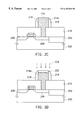
FIGS. 1A and 1B are schematic, cross-sectional views showing the steps according to a conventional method of forming hemispherical silicon grains on the lower electrode surfaces of a capacitor. The storage capacity of the capacitor is thereby increased.
First, as shown in FIG. 1A, a substrate 100 having a field effect transistor 104 thereon is provided. Then, a dielectric layer 110 is formed over the substrate 100 and the field effect transistor 104. Thereafter, a contact opening 112 that exposes a source/drain region 108 is formed in the dielectric layer 110. In the subsequent step, a doped amorphous silicon layer 113 having a thickness of about 6000 Å is deposited, completely fills the contact opening 112, and covers the dielectric layer, as well.
Next, the doped amorphous silicon layer 113 is patterned to form a doped amorphous silicon layer 113 a as shown in FIG. 1B, thereby forming the bulk of the lower electrode of a capacitor. After that, hemispherical silicon grains are formed on the exposed surface of the doped amorphous silicon layer 113 a in order to increase the overall surface area of the lower electrode.
In the aforementioned method, a very thick layer of doped amorphous silicon layer 113 has to be deposited so that a proper electrode structure for the capacitor is formed. However, the rate of deposition of amorphous silicon is rather low, and hence a lot of time is spent in the process of depositing doped amorphous silicon material onto the dielectric layer 110 to a sufficient thickness. The longer the process of depositing amorphous silicon, the slower the production rate of the semiconductor device is.
Furthermore, a long deposition tends to increase the chance of microcrystallization inside the amorphous silicon layer 113. Microcrystallization occurs around nucleation sites, and the nucleation sites are the locations where dopants congregate. The microcrystals inside the amorphous silicon layer tend to limit the growth of hemispherical silicon grains on the lower electrode. Therefore, the ultimate density of the hemispherical silicon grains may decrease considerably.
In other words, the longer the depositing time for the doped amorphous silicon layer 113, the higher the probability of microcrystallization is. The higher the microcrystal density inside the amorphous silicon layer, the lower the quantity of hemispherical silicon grains on the lower electrode surfaces is. Hence, the supposed amount of increase in effective capacitative area is not actually attained.
One method of preventing the formation of too many microcrystals inside a doped amorphous silicon layer 113 is to lower the concentration of dopants during deposition. However, the doped amorphous silicon layer 113 also fills the contact opening 112 so that the source/drain region 108 is electrically connected. Therefore, too few dopants inside the doped amorphous silicon layer 113 results in a high contact resistance between the doped amorphous silicon layer 113 and the source/drain region 108.
In light of the foregoing, there is a need to improve the method of forming a doped amorphous silicon layer so that more hemispherical silicon grains can be formed over the lower electrode surfaces of a capacitor.
SUMMARY OF THE INVENTION
Accordingly, the purpose of the present invention is to provide a method for forming hemispherical silicon grains on the surfaces of a doped amorphous silicon layer such that the density of silicon grains on its surfaces is not affected by microcrystallization at nuclear sites within the doped amorphous silicon layer.
In another aspect, the purpose of this invention is to provide a method for forming hemispherical silicon grains on the lower electrode surfaces of a capacitor such that contact resistance between the lower electrode and a source/drain region is lowered.
To achieve these and other advantages and in accordance with the purpose of the invention, as embodied and broadly described herein, the invention provides a method for forming hemispherical silicon grains on selected surfaces of a silicon layer. The method includes the steps of forming a doped polysilicon layer over a substrate, and then forming amorphous spacers on the sidewalls of the doped polysilicon layer. Thereafter, an ion implantation is carried out to transform the upper portion of the doped polysilicon into an amorphous silicon layer. Finally, hemispherical silicon grains are formed on the upper surface of the amorphous layer lying above the polysilicon layer and the exposed surface of the amorphous spacers.
It is to be understood that both the foregoing general description and the following detailed description are exemplary, and are intended to provide further explanation of the invention as claimed.
BRIEF DESCRIPTION OF THE DRAWINGS
The accompanying drawings are included to provide a further understanding of the invention, and are incorporated in and constitute a part of this specification. The drawings illustrate embodiments of the invention and, together with the description, serve to explain the principles of the invention. In the drawings,
FIGS. 1A and 1B are schematic cross-sectional views showing the steps according to a conventional method of forming hemispherical silicon grains over the lower electrode surfaces of a capacitor; and
FIGS. 2A through 2E are schematic, cross-sectional views showing the progression of manufacturing steps for forming the lower electrode of a capacitor according to one preferred embodiment of this invention.
DESCRIPTION OF THE PREFERRED EMBODIMENTS
Reference will now be made in detail to the present preferred embodiments of the invention, examples of which are illustrated in the accompanying drawings. Wherever possible, the same reference numbers are used in the drawings and the description to refer to the same or like parts.
FIGS. 2A through 2E are schematic, cross-sectional views showing the progression of manufacturing steps for forming the lower electrode of a capacitor according to one preferred embodiment of this invention.
As shown in FIG. 2A, an isolation region 202 is formed in a substrate 200 so that an active region for accommodating a semiconductor device is defined. Thereafter, a field effect transistor 204 is formed in the active region. The field effect transistor 204 includes a gate structure 206 and source/drain regions 208. Next, a dielectric layer 210 is formed over the substrate 200. The dielectric layer can be a silicon oxide or a borophosphosilicate glass (BPSG) layer formed by performing a chemical vapor deposition (CVD) operation. Preferably, a chemical-mechanical polishing operation is carried out to planarize the dielectric layer 210 after it is formed.
As shown in FIG. 2B, conventional photolithographic and etching operations are conducted to pattern the dielectric layer 210 so that a contact opening 212 is formed in the dielectric layer 210. The contact opening 212 exposes one of the source/drain regions 208 in the substrate 200. Subsequently, a doped polysilicon layer 214 is formed over the substrate 200 so that the contact opening 212 is filled and the dielectric layer 210 is covered. The method of forming the doped polysilicon layer 214 includes performing a chemical vapor deposition (CVD) operation. The dopants within the polysilicon layer 214 can be added during the chemical vapor deposition (CVD) operation. Alternatively, the dopants can be added using an ion implantation after the polysilicon layer is formed. The concentration of dopants inside the polysilicon layer 214 is preferably between 5×10²⁰ l/cm3 and 5×10²¹ l/cm3. Conventional photolithographic and etching operations are again used to pattern the doped polysilicon layer 214 into a doped polysilicon layer 214 a as shown in FIG. 2C.
Preferably, the doped polysilicon layer 214 a is cylindrical. Thereafter, amorphous silicon spacers 218 are formed on the sidewalls 216 of the doped polysilicon layer 214 a. The amorphous silicon spacers 218 and the doped polysilicon layer 214 a together form the lower electrode body of a capacitor. The amorphous silicon spacers 218 can be formed by depositing a layer of amorphous silicon having a thickness of between 500 Å and 2500 Å over the dielectric layer 210, using a chemical vapor deposition (CVD) method. Then, the amorphous silicon layer is etched back to expose a portion of the dielectric layer 210 and the upper surface 220 of the doped polysilicon layer 214 a.
As shown in FIG. 2D, the exposed upper surface 220 of the doped polysilicon layer 214 a is transformed into an amorphous layer 222 and a doped polysilicon layer 214 b under the amorphous layer 222. The preferred method of forming the amorphous layer 222 includes performing an ion implantation 224 that bombards dopants directly into the doped polysilicon layer 214 a. Dopants that preferably have a heavy atomic weight, such as arsenic (As), argon (Ar) or antimony (Sb), are implanted into the doped polysilicon layer 214 a. The dopant of heavy atomic weight generally refers to the ions having a large number of nucleons, so that it is easy to transform polysilicon into amorphous silicon, as well known in the art. The energy used in the implantation 224 must be large enough to transform a layer of the doped polysilicon layer 214 a having a thickness of between 500 Å and 1500 Å from the upper surface 220 into amorphous silicon. In other words, the amorphous silicon layer 222 preferably has a thickness of between 500 Å and 1500 Å.
As shown in FIG. 2E, a hemispherical silicon grain layer 226 is formed on the exposed surfaces of the amorphous silicon spacers 218 and on the upper surface of the amorphous silicon layer 222. Hence, surface area of the lower electrode is increased. The exposed amorphous silicon surfaces are preferably first processed with hydrofluoric acid solution to remove any native oxide. Then, hemispherical silicon grains are grown on the amorphous silicon surfaces to form the hemispherical silicon grain layer 226 at a temperature of between 545° C. and 565° C.
In summary, major aspects of this invention includes:
1. A thinner layer of amorphous silicon is deposited for growing hemispherical silicon grains. Since there is no need to deposit a thick layer of amorphous silicon just to build the body of an electrode, both processing time and production cost can be saved.
2. Amorphous spacers are formed on the sidewalls of the doped polysilicon layer prior to transforming the upper layer of the doped polysilicon layer into an amorphous silicon layer by ion bombardment. Since the amorphous silicon spacers are very thin, the required depositing time is relatively short. With a shorter depositing time than the conventional method, fewer microcrystals are formed inside the amorphous silicon layer. Consequently, growth of hemispherical silicon grains on the amorphous silicon surfaces is unhampered.
3. The conventional method uses doped amorphous silicon to fill the contact opening that leads to a source/drain region. Since the level of dopants inside the amorphous silicon must be low to avoid microcrystals formation inside, contact resistance between the electrode and the source/drain terminal is usually high. In this invention, however, heavily doped polysilicon is used to fill the contact opening. Hence, a low contact resistance between the electrode and the source/drain terminal is obtained.
4. Processing operations that need to be carried out in this invention are compatible with current semiconductor processing operations, and therefore they can be readily incorporated into a production line to manufacture semiconductor devices.
It will be apparent to those skilled in the art that various modifications and variations can be made to the structure of the present invention without departing from the scope or spirit of the invention. In view of the foregoing, it is intended that the present invention cover modifications and variations of this invention provided they fall within the scope of the following claims and their equivalents.

Claims (13)

What is claimed is:
1. A method for forming hemispherical silicon grains on a silicon layer, comprising the steps of:
providing a substrate, which has a dielectric layer on top, and has an opening in the dielectric layer to expose the substrate beneath the dielectric layer;
forming a doped polysilicon layer over the substrate, wherein the doped polysilicon layer also fills the opening;
patterning the doped polysilicon layer to remove an undesired portion;
forming amorphous silicon spacers on sidewalls of the doped polysilicon layer;
transforming an upper portion of the doped polysilicon layer into an amorphous silicon layer, wherein the amorphous silicon layer and the amorphous silicon spacer together cover the doped polysilicon layer; and
forming hemispherical silicon grains on an exposed surface of the amorphous silicon spacers and an upper surface of the amorphous silicon layer lying above the doped polysilicon layer.
2. The method of claim 1, wherein the step of transforming the upper portion of the doped polysilicon layer into the amorphous silicon layer includes performing an ion implantation.
3. The method of claim 2, wherein the step of implanting ions includes implanting arsenic ions.
4. The method of claim 2, wherein the step of implanting ions includes implanting argon ions.
5. The method of claim 2, wherein the step of implanting ions includes implanting antimony ions.
6. The method of claim 2, wherein the step of implanting ions into the polysilicon layer to transform the upper portion of the doped polysilicon layer into an amorphous silicon layer includes implanting ions with such an energy level that a layer having a thickness of between 500 Å and 1500 Å from the upper surface of the doped polysilicon layer is completely transformed into an amorphous silicon layer.
7. A method for forming a lower electrode of a capacitor, comprising the steps of:
providing a substrate;
forming a dielectric layer over the substrate, wherein a contact opening that exposes a portion of the substrate is also formed in the dielectric layer;
forming a doped polysilicon layer that fills the contact opening and covers a portion of the dielectric layer;
patterning the doped polysilicon by photolithography;
forming amorphous silicon spacers on sidewalls of the doped polysilicon layer;
performing an ion implantation to transform an upper portion of the doped polysilicon layer into an amorphous silicon layer; and
forming hemispherical silicon grains on an exposed surface of the amorphous silicon spacers and an upper surface of the amorphous silicon layer lying above the doped polysilicon layer.
8. The method of claim 7, wherein the step of performing the ion implantation to transform the upper portion of the doped polysilicon layer into the amorphous silicon layer includes implanting ions into the upper portion of the doped polysilicon layer.
9. The method of claim 8, wherein the step of implanting ions includes implanting arsenic ions.
10. The method of claim 8, wherein the step of implanting ions includes implanting argon ions.
11. The method of claim 8, wherein the step of implanting ions includes implanting antimony ions.
12. The method of claim 7, wherein the step of implanting ions into the polysilicon layer to transform the upper portion of the doped polysilicon layer into an amorphous silicon layer includes implanting ions with such an energy level that a layer having a thickness of between 500 Å and 1500 Å from the upper surface of the doped polysilicon layer is completely transformed into an amorphous silicon layer.
13. The method of claim 7, wherein the doped polysilicon layer can have a cylindrical profile.
US09/241,526 1998-12-04 1999-02-01 Method for forming hemispherical silicon grains on designated areas of silicon layer Expired - Lifetime US6187630B1 (en)

Applications Claiming Priority (2)

Application Number Priority Date Filing Date Title
TW87120145 1998-12-04
TW087120145A TW399235B (en) 1998-12-04 1998-12-04 Selective semi-sphere silicon grain manufacturing method

Publications (1)

Publication Number Publication Date
US6187630B1 true US6187630B1 (en) 2001-02-13

Family

ID=21632189

Family Applications (1)

Application Number Title Priority Date Filing Date
US09/241,526 Expired - Lifetime US6187630B1 (en) 1998-12-04 1999-02-01 Method for forming hemispherical silicon grains on designated areas of silicon layer

Country Status (2)

Country Link
US (1) US6187630B1 (en)
TW (1) TW399235B (en)

Cited By (3)

* Cited by examiner, † Cited by third party
Publication number Priority date Publication date Assignee Title
US6297137B1 (en) * 1999-06-24 2001-10-02 Hyundai Electronics Industries Co., Ltd. Method for forming gate electrode in semiconductor device capable of preventing distortion of oxidation profile thereof
US6472302B1 (en) * 2001-06-12 2002-10-29 Promos Technologies, Inc. Integration method for raised contact formation for sub-150 nm devices
US6977204B1 (en) * 2002-09-25 2005-12-20 Hynix Semiconductor Inc. Method for forming contact plug having double doping distribution in semiconductor device

Citations (6)

* Cited by examiner, † Cited by third party
Publication number Priority date Publication date Assignee Title
US4697333A (en) * 1985-02-20 1987-10-06 Kabushiki Kaisha Toshiba Method of manufacturing a semiconductor device using amorphous silicon as a mask
US5597741A (en) * 1990-09-07 1997-01-28 Canon Kabushiki Kaisha Process for forming a recrystallized layer and diffusing impurities
US5773342A (en) * 1996-05-16 1998-06-30 Nec Corporation Method for forming a storage node in a semiconductor memory using ion implantation to form a smooth amorphous polycrystalline film
US5821157A (en) * 1995-04-17 1998-10-13 Samsung Electronics Co., Ltd. Argon amorphizing polysilicon layer fabrication
US5897352A (en) * 1998-03-25 1999-04-27 Vanguard International Semiconductor Corporation Method of manufacturing hemispherical grained polysilicon with improved adhesion and reduced capacitance depletion
US5915189A (en) * 1997-08-22 1999-06-22 Samsung Electronics Co., Ltd. Manufacturing method for semiconductor memory device having a storage node with surface irregularities

Patent Citations (6)

* Cited by examiner, † Cited by third party
Publication number Priority date Publication date Assignee Title
US4697333A (en) * 1985-02-20 1987-10-06 Kabushiki Kaisha Toshiba Method of manufacturing a semiconductor device using amorphous silicon as a mask
US5597741A (en) * 1990-09-07 1997-01-28 Canon Kabushiki Kaisha Process for forming a recrystallized layer and diffusing impurities
US5821157A (en) * 1995-04-17 1998-10-13 Samsung Electronics Co., Ltd. Argon amorphizing polysilicon layer fabrication
US5773342A (en) * 1996-05-16 1998-06-30 Nec Corporation Method for forming a storage node in a semiconductor memory using ion implantation to form a smooth amorphous polycrystalline film
US5915189A (en) * 1997-08-22 1999-06-22 Samsung Electronics Co., Ltd. Manufacturing method for semiconductor memory device having a storage node with surface irregularities
US5897352A (en) * 1998-03-25 1999-04-27 Vanguard International Semiconductor Corporation Method of manufacturing hemispherical grained polysilicon with improved adhesion and reduced capacitance depletion

Cited By (3)

* Cited by examiner, † Cited by third party
Publication number Priority date Publication date Assignee Title
US6297137B1 (en) * 1999-06-24 2001-10-02 Hyundai Electronics Industries Co., Ltd. Method for forming gate electrode in semiconductor device capable of preventing distortion of oxidation profile thereof
US6472302B1 (en) * 2001-06-12 2002-10-29 Promos Technologies, Inc. Integration method for raised contact formation for sub-150 nm devices
US6977204B1 (en) * 2002-09-25 2005-12-20 Hynix Semiconductor Inc. Method for forming contact plug having double doping distribution in semiconductor device

Also Published As

Publication number Publication date
TW399235B (en) 2000-07-21

Similar Documents

Publication Publication Date Title
US6365452B1 (en) DRAM cell having a vertical transistor and a capacitor formed on the sidewalls of a trench isolation
US6291289B2 (en) Method of forming DRAM trench capacitor with metal layer over hemispherical grain polysilicon
US6385020B1 (en) Methods of forming HSG capacitors from nonuniformly doped amorphous silicon layers and HSG capacitors formed thereby
US5994197A (en) Method for manufacturing dynamic random access memory capable of increasing the storage capacity of the capacitor
WO1999004434A2 (en) Hemispherical grained polysilicon semiconductor capacitor structure and method
US6037219A (en) One step in situ doped amorphous silicon layers used for selective hemispherical grain silicon formation for crown shaped capacitor applications
US5656529A (en) Method for manufacturing highly-integrated capacitor
US5665624A (en) Method for fabricating trench/stacked capacitors on DRAM cells with increased capacitance
US6054394A (en) Method of fabricating a dynamic random access memory capacitor
US6127221A (en) In situ, one step, formation of selective hemispherical grain silicon layer, and a nitride-oxide dielectric capacitor layer, for a DRAM application
US20020008272A1 (en) Method for fabricating a DRAM cell capacitor using hemispherical grain (HSG) silicon
US6187630B1 (en) Method for forming hemispherical silicon grains on designated areas of silicon layer
JP2000058790A (en) Semiconductor device and manufacture therefor
US5976977A (en) Process for DRAM capacitor formation
US6432772B1 (en) Method of forming a lower storage node of a capacitor
KR20000000685A (en) Method for manufacturing capacitors having hemi-spherical grains
US6004859A (en) Method for fabricating a stack capacitor
US7238585B2 (en) Method of forming a storage electrode of a semiconductor device
US6399440B1 (en) Method to reduce the node contact resistance
KR100379331B1 (en) Bottom electrode of capacitor and fabricating method thereof
US6391714B2 (en) Method for fabricating a capacitor in a semiconductor memory device
US6828207B2 (en) Method of Fabricating a capacitor structure having hemispherical grains
JP3407022B2 (en) Semiconductor device, method of manufacturing the same, and semiconductor storage device
KR100301735B1 (en) Method of manufacturing semiconductor device
US6204121B1 (en) Method for bottom electrode of capacitor

Legal Events

Date Code Title Description
AS Assignment

Owner name: UNITED SEMICONDUCTOR CORP., TAIWAN

Free format text: ASSIGNMENT OF ASSIGNORS INTEREST;ASSIGNORS:CHEN, ANCHOR;CHEN, SHIH-CHING;REEL/FRAME:009747/0965;SIGNING DATES FROM 19981230 TO 19990112

AS Assignment

Owner name: UNITED MICROELECTRONICS CORP., TAIWAN

Free format text: ASSIGNMENT OF ASSIGNORS INTEREST;ASSIGNOR:UNITED SEMICONDUCTOR CORP.;REEL/FRAME:010579/0570

Effective date: 19991230

STCF Information on status: patent grant

Free format text: PATENTED CASE

FPAY Fee payment

Year of fee payment: 4

FPAY Fee payment

Year of fee payment: 8

FPAY Fee payment

Year of fee payment: 12