US6184752B1 - Amplifier device with digitally controllable gain and optical disc read apparatus incorporating such a device - Google Patents
Amplifier device with digitally controllable gain and optical disc read apparatus incorporating such a device Download PDFInfo
- Publication number
- US6184752B1 US6184752B1 US09/413,393 US41339399A US6184752B1 US 6184752 B1 US6184752 B1 US 6184752B1 US 41339399 A US41339399 A US 41339399A US 6184752 B1 US6184752 B1 US 6184752B1
- Authority
- US
- United States
- Prior art keywords
- sources
- output
- current
- digital
- signal
- Prior art date
- Legal status (The legal status is an assumption and is not a legal conclusion. Google has not performed a legal analysis and makes no representation as to the accuracy of the status listed.)
- Expired - Lifetime
Links
Images


Classifications
-
- H—ELECTRICITY
- H03—ELECTRONIC CIRCUITRY
- H03G—CONTROL OF AMPLIFICATION
- H03G1/00—Details of arrangements for controlling amplification
- H03G1/0005—Circuits characterised by the type of controlling devices operated by a controlling current or voltage signal
- H03G1/0088—Circuits characterised by the type of controlling devices operated by a controlling current or voltage signal using discontinuously variable devices, e.g. switch-operated
-
- G—PHYSICS
- G11—INFORMATION STORAGE
- G11B—INFORMATION STORAGE BASED ON RELATIVE MOVEMENT BETWEEN RECORD CARRIER AND TRANSDUCER
- G11B7/00—Recording or reproducing by optical means, e.g. recording using a thermal beam of optical radiation by modifying optical properties or the physical structure, reproducing using an optical beam at lower power by sensing optical properties; Record carriers therefor
- G11B7/004—Recording, reproducing or erasing methods; Read, write or erase circuits therefor
- G11B7/005—Reproducing
-
- G—PHYSICS
- G11—INFORMATION STORAGE
- G11B—INFORMATION STORAGE BASED ON RELATIVE MOVEMENT BETWEEN RECORD CARRIER AND TRANSDUCER
- G11B7/00—Recording or reproducing by optical means, e.g. recording using a thermal beam of optical radiation by modifying optical properties or the physical structure, reproducing using an optical beam at lower power by sensing optical properties; Record carriers therefor
- G11B7/08—Disposition or mounting of heads or light sources relatively to record carriers
- G11B7/09—Disposition or mounting of heads or light sources relatively to record carriers with provision for moving the light beam or focus plane for the purpose of maintaining alignment of the light beam relative to the record carrier during transducing operation, e.g. to compensate for surface irregularities of the latter or for track following
- G11B7/0941—Methods and circuits for servo gain or phase compensation during operation
Definitions
- the present invention relates to an amplifier with digitally controlled gain and its application to a circuit for processing signals output by a read head of an optical disc reader apparatus.
- information recorded on an optical disc 1 is read, in a manner which is known per se, by projecting a light beam 3 output by a laser diode 2 onto the reflective surface of the disc.
- the reflected beam 4 is detected by photodiodes A, B, C, D, E and F, the signals output by these photodiodes being used, inter alia, to decode the information stored on the optical disc.
- the photodiodes A to F, as well as the laser diode 2 form part of an optical and mechanical assembly 5 referred to as the read head of the apparatus, or optical pick-up, which does not form the subject-matter of the present invention and will not be described in further detail.
- the signals output by the photodiodes A and C are added before being processed. The same is true of the signals output by the photodiodes B and D.
- Four signals S 0 to S 3 thus leave the read head 5 to be processed and decoded by a suitable processing circuit.
- the signals S 0 to S 3 correspond to the currents flowing through the photodiodes. These currents vary as a function of a certain number of factors, such as the reflectivity of the surface of the disc (depending on its state of cleanliness) or the power of the emitting laser diode 2 .
- Fixed-gain current/current amplifiers 10 to 13 receive the signals S 0 to S 3 and are connected to the four inputs E 0 to E 3 of a multiplexer 15 .
- the output of the multiplexer 15 is connected to a resistor 16 , which converts the current into voltage, and to the input of analogue/digital converter 18 which delivers a digital signal encoded using six bits to a digital circuit 25 for processing and decoding the signals emitted by the photodiodes.
- the signal entering the converter In order to make maximum use of the dynamic range of the analogue/digital converter 18 , and thus to deliver high-quality signals to the circuit 25 , it is necessary for the signal entering the converter to have a sufficient amplitude. However, this amplitude depends directly on the current which is picked up by the photodiodes A to F. Depending on the type of read head which is used, the amplitude of the signal received by the analogue/digital converter 18 can vary from one to four times. These large variations are corrected by modifying the value of the resistor 16 as a function of the type of read head used. To that end, when the circuit for processing the signals output by the read head 5 is produced in integrated circuit form, a pin is provided on the circuit in order to make it possible to connect an external resistor 16 of suitable value to the read head.
- the value of the resistor 16 is fixed for each given type of read head and does not make it possible to correct smaller but all the same significant variations in the current output by the photodiodes, which variations are due to the surface condition of the optical disc 1 , which is not uniform (fingerprints, etc.) or the conditions under which the apparatus is being used (temperature, background light, etc.).
- FIGS. 2 a to 2 c illustrate different ways of adjusting the gain of an amplifier.
- the amplifiers are voltage-controlled.
- an input signal V IN1 is applied to one of the gates of a two-gate MOSFET transistor 36 whose drain is connected to a supply V DD via a resistor 34 and whose source is earthed.
- the drain of the transistor 36 is also connected to an operational amplifier 37 , set up in follower mode, whose output is connected to the input of an analogue/digital converter 38 which delivers a digital signal to a digital processing circuit 35 .
- the transconductance of the transistor 36 will be modified by applying, to the second gate of the transistor, a control voltage V COM1 coming from a return loop.
- the return loop is formed by a digital signal leaving the circuit 35 sent to a digital/analogue converter 39 whose output is connected to an operational amplifier 37 ′, set up in follower mode, which delivers at an output the control voltage V COM1 .
- the problem with this device is that the gain does not vary linearly as a function of the control voltage throughout the adjustment range of the gain.
- FIG. 2 b elements which are identical have the same references as in FIG. 2 a .
- the input signal V IN2 is applied to a first non-inverting input of an operational amplifier 47 whose inverting input is earthed via a resistor 44 and which has a feedback loop connecting its output to its inverting input via a MOS transistor 46 set up in triode mode.
- the gain of the amplifier is modified by a control voltage V COM2 (taken from the output of the operational amplifier 37 ′) which modifies the value of the resistor formed by the MOS transistor 46 .
- V COM2 control voltage
- This device although it makes it possible to obtain a more linear variation in the gain, nevertheless has stability problems due to the feedback loop formed by the MOS transistor.
- the voltage for controlling the gain comes from a digital/analogue converter 39 which occupies a large amount of space, in particular when the assembly is produced in integrated circuit form.
- a network of resistors 56 is placed in the feedback path of an amplifier 57 which receives the input signal V IN3 .
- the resistors 56 may or may not be connected in parallel using switching devices 59 which are controlled directly by a digital signal V COM3 output by the digital processing circuit 35 .
- the gain is adjusted by connecting a greater or lesser number of resistors in the feedback path.
- the controlled-gain amplifiers of the prior art cannot be used satisfactorily in the systems for processing the signals S 0 to S 3 in FIG. 1 in order to adjust the amplitude of the signals delivered to the mulitplexer 15 and therefore to the analogue/digital converter 18 .
- the object of the invention is to solve the various problems which have been explained above.
- variable-gain amplifier device controlled by a digital signal which has:
- the number of sources which are connected in the first and second series of current sources is controlled by the digital signal and determines the gain of the device.
- the gain of the amplifier device is thus controlled directly by a digital signal and, since the device does not have a feedback loop, it is perfectly stable.
- the invention also relates to an apparatus for reading optical discs, having a laser diode for emitting a light beam and photodiodes designed to pick up the light beam reflected by an optical disc when it is placed in the apparatus, the signals output by the photodiodes being processed in processing systems before being sent to an analogue/digital converter whose output is connected to a digital circuit.
- the processing systems of the apparatus have a variable-gain amplifier device controlled by a digital signal output by the circuit such as that described above for matching the signals sent to the input of the analogue/digital converter to the dynamic range of the converter.
- the current flowing through the laser diode of the apparatus is roughly constant. Its life is thus extended by this.
- FIG. 1 already described above, schematically illustrates a part of an optical disc reader apparatus according to the prior art
- FIGS. 2 a to 2 c also described above, represent three analogue/digital processing systems of the prior art having a gain adjustment stage;
- FIG. 3 represents an amplifier device with digitally controllable gain according to a first embodiment of the invention
- FIG. 4 represents an amplifier device with digitally controllable gain according to a second embodiment of the invention
- FIG. 5 illustrates a part of an optical disc reader apparatus implementing the invention.
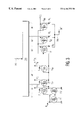
- FIG. 3 represents a current/current amplifier which receives as input a current I IN and delivers as output a current I OUT as a function of a digital control signal 200 .
- the input current I IN is applied to a current mirror formed by the N-channel MOS transistors 201 and 202 . More precisely, the current I IN is applied to the drain of the transistor 201 which is connected to its gate, itself connected to the gate of the transistor 202 .
- the drain-source current of the transistor 202 is therefore equal to I IN.
- a first series of M current sources which consist of P-channel MOS transistors T 71 , T 72 , T 7M is arranged in such a way that the sum of the currents of these sources is equal to I IN .
- All the gates of the transistors T 71 to T 7M are connected respectively to the drains of the same transistors, which are themselves connected to the drain of the transistor 202 .
- All the sources of the transistors T 71 to T 7M are connected to a supply voltage V CC through a series of switches 171 , 172 , 17 M.
- the switches 171 to 17 M are controlled by respective binary instructions a1, a2, aM constructed on the basis of the digital control signal 200 by a control logic circuit 210 .
- the drain-source current of the transistor 202 which is equal to I IN , is thus divided between the M current sources. If all the switches 171 to 17 M are closed, the source-drain current flowing through each of the transistors T 71 to T 7M is equal to I IN /M. Conversely, if only two switches out of the M are closed, then the current flowing through the corresponding transistors is equal to I IN /2.
- a second series of N current sources which consist of P-channel MOS transistors T 81 , T 82 , T 8N is arranged to form a current mirror with the first series of M sources. That is to say all the gates of the transistors Tel to T 8N are connected to the common point of the gates and drains of the first transistor T 71 to T 7M .
- the sources of the transistors T 81 to T 8N are connected to the supply voltage V cc and the drains of the transistors are each connected to a first terminal of a respective switch 181 , 182 , 18 N, the second terminals of all the switches 181 to 18 N being connected together to form a node to which a wire 205 delivering the output current of the amplifier I OUT is connected.
- the switches 181 to 18 N are controlled by the respective binary instructions b1, b2, bN which are constructed on the basis of the digital control signal 200 by the control logic circuit 210 .
- the amplifier of the invention has no stability problem because it does not have any feedback loop.
- the purpose of the controlled-gain amplifier of the invention is to output a signal with quasi-constant amplitude corresponding to an optimum value allowing best use to be made of the dynamic range of an analogue/digital converter arranged at the output of the amplifier, whatever the amplitude of the input signal of the amplifier is.
- the minimum variation increment of I OUT corresponds to the current flowing through one of the output sources T 81 to T 8N , that is to say I IN /m, assuming that m switches controlling the reference sources are closed.
- the digital control signal 200 is a signal encoded using N c bits.
- the number n of closed switches out of the control switches of the output sources varies linearly from 1 to N c .
- the integer part of the number given by equation (3) will be taken.
- the number of bits N c of the instruction will therefore be adapted as a function of the dynamic range of the input current I IN , according to the precision which it is desired to obtain.
- a digital control signal 200 encoded using 6 bits is used, that is to say one which can assume 64 different values.
- the code “0” is received, all the reference sources are connected (all the switches 17 x are closed) and when the code 63 is received, only one reference source is connected (only switch 171 is closed).
- the strategy for controlling the reference and output sources as a function of the code received in the signal 200 can be summarized in Table 2 below, in which the binary instructions a1 to aM and b1 to bN assume the value of “1” when the switch which they control is to be closed, and the value “0” when the switch is to be open.
- control modes may also be envisaged.
- the number of reference sources may be reduced in order to minimize the area of the circuit and simplify the control. Provision may also be made for a certain number of reference sources to remain permanently connected. What is required in practice is to find a compromise between the specifications expected of the circuit (expected output current I OUT , maximum increment allowed in variation of the output current, etc.) and the size of the circuit as a function of the dynamic range of the input current.
- FIG. 4 represents such an amplifier, which receives an input voltage V IN and which delivers at its output a voltage V OUT which is a function of a digital control signal 200 . All the elements which are identical to those in FIG. 3 have identical references, and will not be described further. Only the input and output stages differ from those in FIG. 3 .
- the voltage V IN is applied to the non-inverting input of an operational amplifier 203 .
- the output of the amplifier is connected to the gate of an N-channel MOS transistor 204 , while its inverting input is connected to the source of the transistor 204 and to the first terminal of a resistor 206 , the second terminal of which is earthed.
- the voltage V IN is therefore also found across the terminals of the resistor 206 through which a current I′ IN proportional to V IN flows, this current I′ IN also being equal to the drain-source current of the transistor 204 .
- This transistor 204 fulfils the same function as the transistor 202 of the amplifier represented in FIG. 3 .
- the current I OUT passes through a resistor 207 , one terminal of which is earthed in order, at the other terminal of the resistor, to deliver the output voltage V OUT .
- the way in which the amplifier in FIG. 4 operates is identical to that in FIG. 3 .
- FIG. 5 represents a part of an optical disc reader device which advantageously incorporates the amplifier which was described in FIG. 3 .
- Elements which are similar to those in FIG. 1 which has already been described have the same references and will not be described again.
- the read head 5 delivers four signals S′ 0 , S′ 1 , S′ 2 and S′ 3 which correspond to the currents output by the photodiodes A to F. These signals are processed in four identical processing systems which lead to the four inputs E′ 0 , E′ 1 , E′ 2 and E′ 3 of a multiplexer 115 .
- the processing systems each have a fixed-gain current/current amplifier 110 to 113 , followed by a controlled-gain amplifier 30 to 33 such as the one which is described in FIG. 3, a circuit 40 to 43 controlling the offset of the signal which is arranged at the output of the controlled-gain amplifier, and a resistor 50 to 53 which makes it possible to convert the current into voltage in order to apply it to an operational amplifier 60 to 63 , set up in follower mode, whose output is connected to the input E′ 0 to E′ 3 of the multiplexer 115 .
- the output of the multiplexer 115 which is a voltage signal, is sent to the input of an analogue/digital converter 118 which delivers a digital signal encoded using 6 bits to a digital circuit 125 for processing and decoding the signals output by the photodiodes.
- the operational amplifiers 60 to 63 which are arranged at the end of the systems for processing the signals S′ 0 to S′ 3 fulfil the function of buffers to prevent mixing, or crosstalk, between the channels of the multiplexer 115 . It will be noted that, in contrast to the prior art device represented in FIG. 1, the current/voltage conversion of the signals S′ 0 to S′ 3 is carried out before the signals are multiplexed. This is because, since the variable-gain amplifiers 30 - 33 make it possible to modify the amplitude of the signals directly in the processing system, it is no longer necessary to provide an external resistor whose value is selected according to the type of read head.
- the controlled-gain amplifiers 30 - 33 make it possible both to correct the variations in amplitude of the signals S′ 0 -S′ 3 which are due to the different types of read heads used, and those which are due to the surface condition of the optical disc 1 or other factors. Since the amplifiers 30 - 33 are controlled directly by a digital control signal 108 , constructed by the circuit 125 as a function of the signal received from the analogue/digital converter 118 , it is no longer necessary to provide an extra digital/analogue converter, and it is furthermore no longer necessary to vary the current through the laser diode 2 . The circuit is therefore more compact and the laser diode 2 , whose current is kept constant, has a longer life than in the prior art.
- the amplifier with digitally controlled gain as described in FIG. 3 can be used in applications other than the circuit for processing the signals output by a read head of an optical disc reader. In particular, it can be used in the processing of video signals or audio signals output by tuners.
Landscapes
- Analogue/Digital Conversion (AREA)
- Amplifiers (AREA)
- Control Of Amplification And Gain Control (AREA)
Applications Claiming Priority (2)
| Application Number | Priority Date | Filing Date | Title |
|---|---|---|---|
| FR9812495A FR2784820B1 (fr) | 1998-10-06 | 1998-10-06 | Dispositif amplificateur a gain commandable numeriquement et appareil lecteur de disques optiques incorporant un tel dispositif |
| FR9812495 | 1998-10-06 |
Publications (1)
| Publication Number | Publication Date |
|---|---|
| US6184752B1 true US6184752B1 (en) | 2001-02-06 |
Family
ID=9531240
Family Applications (1)
| Application Number | Title | Priority Date | Filing Date |
|---|---|---|---|
| US09/413,393 Expired - Lifetime US6184752B1 (en) | 1998-10-06 | 1999-10-06 | Amplifier device with digitally controllable gain and optical disc read apparatus incorporating such a device |
Country Status (6)
| Country | Link |
|---|---|
| US (1) | US6184752B1 (enExample) |
| EP (1) | EP0993110B1 (enExample) |
| JP (1) | JP4755743B2 (enExample) |
| CN (1) | CN1158651C (enExample) |
| DE (1) | DE69931231T2 (enExample) |
| FR (1) | FR2784820B1 (enExample) |
Cited By (7)
| Publication number | Priority date | Publication date | Assignee | Title |
|---|---|---|---|---|
| US20030112727A1 (en) * | 2001-12-14 | 2003-06-19 | Takanori Okuda | Photo-detector amplifier circuit for optical disk device |
| US6756576B1 (en) * | 2000-08-30 | 2004-06-29 | Micron Technology, Inc. | Imaging system having redundant pixel groupings |
| US20050248329A1 (en) * | 2004-05-06 | 2005-11-10 | Yukio Sato | Current voltage converter circuit |
| US20060220743A1 (en) * | 2005-03-30 | 2006-10-05 | Iwao Kojima | Variable gain amplifier, mixer and quadrature modulator using the same |
| CN100378812C (zh) * | 2003-02-27 | 2008-04-02 | 三星电子株式会社 | 根据光盘旋转速度控制放大增益的光信号转换器 |
| US20130154705A1 (en) * | 2011-12-15 | 2013-06-20 | Canon Kabushiki Kaisha | Electronic device |
| US9276021B2 (en) | 2011-12-15 | 2016-03-01 | Canon Kabushiki Kaisha | Electronic device including current sources and amplifiers |
Families Citing this family (4)
| Publication number | Priority date | Publication date | Assignee | Title |
|---|---|---|---|---|
| FR2820907A1 (fr) * | 2001-02-13 | 2002-08-16 | St Microelectronics Sa | Circuit de normalisation a tension d'erreur reduite |
| CN100527609C (zh) * | 2005-10-26 | 2009-08-12 | 威盛电子股份有限公司 | 可变增益放大电路及相关方法 |
| JP4883674B2 (ja) * | 2006-01-05 | 2012-02-22 | 株式会社山武 | 受光アンプ |
| US7643573B2 (en) * | 2006-03-17 | 2010-01-05 | Cirrus Logic, Inc. | Power management in a data acquisition system |
Citations (10)
| Publication number | Priority date | Publication date | Assignee | Title |
|---|---|---|---|---|
| US4064506A (en) | 1976-04-08 | 1977-12-20 | Rca Corporation | Current mirror amplifiers with programmable current gains |
| US4250461A (en) | 1979-04-20 | 1981-02-10 | Rca Corporation | Current mirror amplifier |
| US4439673A (en) | 1981-08-27 | 1984-03-27 | Sprague Electric Company | Two terminal integrated circuit light-sensor |
| US4485301A (en) | 1982-02-01 | 1984-11-27 | Sprague Electric Company | Linear two-terminal integrated circuit photo sensor |
| EP0577265A2 (en) | 1992-05-29 | 1994-01-05 | Sharp Kabushiki Kaisha | Light-receiving and amplifying device capable of widening an a.c. operation range |
| US5373253A (en) * | 1993-09-20 | 1994-12-13 | International Business Machines Corporation | Monolithic current mirror circuit employing voltage feedback for β-independent dynamic range |
| US5446397A (en) * | 1992-02-26 | 1995-08-29 | Nec Corporation | Current comparator |
| WO1996007927A2 (en) | 1994-09-01 | 1996-03-14 | Philips Electronics N.V. | Transconductance amplifier having a digitally variable transconductance as well as a variable gain stage and an automatic gain control circuit comprising such a variable gain stage |
| EP0840299A1 (en) | 1996-10-30 | 1998-05-06 | Deutsche Thomson-Brandt Gmbh | Input signal amplifier |
| US5753903A (en) * | 1996-11-05 | 1998-05-19 | Medar, Inc. | Method and system for controlling light intensity in a machine vision system |
Family Cites Families (5)
| Publication number | Priority date | Publication date | Assignee | Title |
|---|---|---|---|---|
| US3940760A (en) * | 1975-03-21 | 1976-02-24 | Analog Devices, Inc. | Digital-to-analog converter with current source transistors operated accurately at different current densities |
| JPS61285808A (ja) * | 1985-06-11 | 1986-12-16 | Sharp Corp | 電流増幅回路 |
| JPH0348506A (ja) * | 1989-04-19 | 1991-03-01 | Nec Corp | 電流可変回路 |
| FR2733098B1 (fr) * | 1995-04-11 | 1997-07-04 | Sgs Thomson Microelectronics | Amplificateur de courant |
| JPH1093436A (ja) * | 1996-09-19 | 1998-04-10 | Oki Electric Ind Co Ltd | デジタル・アナログ変換回路 |
-
1998
- 1998-10-06 FR FR9812495A patent/FR2784820B1/fr not_active Expired - Fee Related
-
1999
- 1999-09-17 DE DE69931231T patent/DE69931231T2/de not_active Expired - Lifetime
- 1999-09-17 EP EP99402282A patent/EP0993110B1/en not_active Expired - Lifetime
- 1999-09-22 CN CNB991194179A patent/CN1158651C/zh not_active Expired - Fee Related
- 1999-10-05 JP JP28473299A patent/JP4755743B2/ja not_active Expired - Fee Related
- 1999-10-06 US US09/413,393 patent/US6184752B1/en not_active Expired - Lifetime
Patent Citations (10)
| Publication number | Priority date | Publication date | Assignee | Title |
|---|---|---|---|---|
| US4064506A (en) | 1976-04-08 | 1977-12-20 | Rca Corporation | Current mirror amplifiers with programmable current gains |
| US4250461A (en) | 1979-04-20 | 1981-02-10 | Rca Corporation | Current mirror amplifier |
| US4439673A (en) | 1981-08-27 | 1984-03-27 | Sprague Electric Company | Two terminal integrated circuit light-sensor |
| US4485301A (en) | 1982-02-01 | 1984-11-27 | Sprague Electric Company | Linear two-terminal integrated circuit photo sensor |
| US5446397A (en) * | 1992-02-26 | 1995-08-29 | Nec Corporation | Current comparator |
| EP0577265A2 (en) | 1992-05-29 | 1994-01-05 | Sharp Kabushiki Kaisha | Light-receiving and amplifying device capable of widening an a.c. operation range |
| US5373253A (en) * | 1993-09-20 | 1994-12-13 | International Business Machines Corporation | Monolithic current mirror circuit employing voltage feedback for β-independent dynamic range |
| WO1996007927A2 (en) | 1994-09-01 | 1996-03-14 | Philips Electronics N.V. | Transconductance amplifier having a digitally variable transconductance as well as a variable gain stage and an automatic gain control circuit comprising such a variable gain stage |
| EP0840299A1 (en) | 1996-10-30 | 1998-05-06 | Deutsche Thomson-Brandt Gmbh | Input signal amplifier |
| US5753903A (en) * | 1996-11-05 | 1998-05-19 | Medar, Inc. | Method and system for controlling light intensity in a machine vision system |
Non-Patent Citations (1)
| Title |
|---|
| French Search Report citing the above-listed references: AA, AB, AC, AD, and AM. |
Cited By (18)
| Publication number | Priority date | Publication date | Assignee | Title |
|---|---|---|---|---|
| US6756576B1 (en) * | 2000-08-30 | 2004-06-29 | Micron Technology, Inc. | Imaging system having redundant pixel groupings |
| US20040222356A1 (en) * | 2000-08-30 | 2004-11-11 | Micron Technology, Inc. | Redundant imaging methods and systems |
| US20040222355A1 (en) * | 2000-08-30 | 2004-11-11 | Micron Technology, Inc. | Redundant imaging methods and systems |
| US7129457B2 (en) | 2000-08-30 | 2006-10-31 | Micron Technology, Inc. | Redundant imaging systems |
| US7297915B2 (en) | 2000-08-30 | 2007-11-20 | Micron Technology, Inc. | Compensation methods and systems for imaging detectors |
| US7263046B2 (en) | 2001-12-14 | 2007-08-28 | Sharp Kabushiki Kaisha | Photo-detector amplifier circuit for optical disk device |
| CN100409332C (zh) * | 2001-12-14 | 2008-08-06 | 夏普公司 | 光盘装置的受光放大器电路 |
| US20030112727A1 (en) * | 2001-12-14 | 2003-06-19 | Takanori Okuda | Photo-detector amplifier circuit for optical disk device |
| US7133346B2 (en) * | 2001-12-14 | 2006-11-07 | Sharp Kabushiki Kaisha | Photo-detector amplifier circuit for optical disk device |
| US20070019517A1 (en) * | 2001-12-14 | 2007-01-25 | Sharp Kabushiki Kaisha | Photo-detector amplifier circuit for optical disk device |
| CN100378812C (zh) * | 2003-02-27 | 2008-04-02 | 三星电子株式会社 | 根据光盘旋转速度控制放大增益的光信号转换器 |
| US7227119B2 (en) * | 2004-05-06 | 2007-06-05 | Kabushiki Kaisha Toshiba | Current voltage converter circuit |
| US20050248329A1 (en) * | 2004-05-06 | 2005-11-10 | Yukio Sato | Current voltage converter circuit |
| US20060220743A1 (en) * | 2005-03-30 | 2006-10-05 | Iwao Kojima | Variable gain amplifier, mixer and quadrature modulator using the same |
| US7432765B2 (en) | 2005-03-30 | 2008-10-07 | Matsushita Electric Industrial Co., Ltd. | Variable gain amplifier, mixer and quadrature modulator using the same |
| US20130154705A1 (en) * | 2011-12-15 | 2013-06-20 | Canon Kabushiki Kaisha | Electronic device |
| US9276021B2 (en) | 2011-12-15 | 2016-03-01 | Canon Kabushiki Kaisha | Electronic device including current sources and amplifiers |
| US9356585B2 (en) * | 2011-12-15 | 2016-05-31 | Canon Kabushiki Kaisha | Image pickup device |
Also Published As
| Publication number | Publication date |
|---|---|
| CN1250209A (zh) | 2000-04-12 |
| EP0993110A1 (en) | 2000-04-12 |
| CN1158651C (zh) | 2004-07-21 |
| JP4755743B2 (ja) | 2011-08-24 |
| DE69931231T2 (de) | 2007-02-22 |
| EP0993110B1 (en) | 2006-05-10 |
| DE69931231D1 (de) | 2006-06-14 |
| JP2000201037A (ja) | 2000-07-18 |
| FR2784820A1 (fr) | 2000-04-21 |
| FR2784820B1 (fr) | 2000-12-08 |
Similar Documents
| Publication | Publication Date | Title |
|---|---|---|
| US6184752B1 (en) | Amplifier device with digitally controllable gain and optical disc read apparatus incorporating such a device | |
| JP3152922B2 (ja) | 電流ミラー回路 | |
| US5914622A (en) | Pulse-width controller | |
| US5283579A (en) | Digital to analog converter having high multiplying bandwidth | |
| US6222357B1 (en) | Current output circuit with controlled holdover capacitors | |
| US5596285A (en) | Impedance adaptation process and device for a transmitter and/or receiver, integrated circuit and transmission system | |
| US6288564B1 (en) | Line receiver circuit with line termination impedance | |
| US6580326B2 (en) | High-bandwidth low-voltage gain cell and voltage follower having an enhanced transconductance | |
| US5191297A (en) | Transconductance amplifier having sensfets which drive a load with linearly proportional current | |
| US5764174A (en) | Switch architecture for R/2R digital to analog converters | |
| US7710169B2 (en) | Semiconductor integrated circuit controlling output impedance and slew rate | |
| US5763924A (en) | Circuits and methods for compensating non-linear capacitances to minimize harmonic distortion | |
| JPH05191162A (ja) | 演算増幅器および回線終端装置 | |
| EP0693749A1 (en) | A bidirectional load current sense circuit for a H-bridge | |
| US6255910B1 (en) | Active operating point adjustment for power amplifiers | |
| US5859564A (en) | Differential amplifier circuit for use in a read channel for a magnetic recording system | |
| US6331803B1 (en) | Constant bandwidth, variable gain amplifier, and method | |
| JPH04181817A (ja) | スイッチング定電流源回路 | |
| US20050017784A1 (en) | Variable gain amplifier and a large scale integrated circuit installed thereof applicable to processing signals | |
| KR970005825B1 (ko) | 차동 전류원 회로 | |
| JP2560542B2 (ja) | 電圧電流変換回路 | |
| EP0874453A2 (en) | Programmable amplifier | |
| US20050003784A1 (en) | Attenuator and portable telephone terminal apparatus using the same | |
| KR20010071056A (ko) | 증폭기 출력단 | |
| US5334950A (en) | Class-AB push-pull drive circuit |
Legal Events
| Date | Code | Title | Description |
|---|---|---|---|
| AS | Assignment |
Owner name: THOMSOM MULTIMEDIA, FRANCE Free format text: ASSIGNMENT OF ASSIGNORS INTEREST;ASSIGNOR:DAUTRICHE, PIERRE;REEL/FRAME:010306/0350 Effective date: 19990928 |
|
| AS | Assignment |
Owner name: THOMSON LICENSING S.A., FRANCE Free format text: ASSIGNMENT OF ASSIGNORS INTEREST;ASSIGNOR:THOMSON MULTIMEDIA;REEL/FRAME:011141/0281 Effective date: 20001130 |
|
| STCF | Information on status: patent grant |
Free format text: PATENTED CASE |
|
| FPAY | Fee payment |
Year of fee payment: 4 |
|
| FPAY | Fee payment |
Year of fee payment: 8 |
|
| FPAY | Fee payment |
Year of fee payment: 12 |
|
| AS | Assignment |
Owner name: MAGNOLIA LICENSING LLC, TEXAS Free format text: ASSIGNMENT OF ASSIGNORS INTEREST;ASSIGNOR:THOMSON LICENSING S.A.S.;REEL/FRAME:053570/0237 Effective date: 20200708 |