US6169449B1 - Transmission power control circuit capable of varying electric power over a wide range - Google Patents
Transmission power control circuit capable of varying electric power over a wide range Download PDFInfo
- Publication number
- US6169449B1 US6169449B1 US09/345,030 US34503099A US6169449B1 US 6169449 B1 US6169449 B1 US 6169449B1 US 34503099 A US34503099 A US 34503099A US 6169449 B1 US6169449 B1 US 6169449B1
- Authority
- US
- United States
- Prior art keywords
- circuit
- transmission
- circulator
- signal
- control circuit
- Prior art date
- Legal status (The legal status is an assumption and is not a legal conclusion. Google has not performed a legal analysis and makes no representation as to the accuracy of the status listed.)
- Expired - Lifetime
Links
Images


Classifications
-
- H—ELECTRICITY
- H03—ELECTRONIC CIRCUITRY
- H03F—AMPLIFIERS
- H03F3/00—Amplifiers with only discharge tubes or only semiconductor devices as amplifying elements
- H03F3/72—Gated amplifiers, i.e. amplifiers which are rendered operative or inoperative by means of a control signal
-
- H—ELECTRICITY
- H03—ELECTRONIC CIRCUITRY
- H03F—AMPLIFIERS
- H03F1/00—Details of amplifiers with only discharge tubes, only semiconductor devices or only unspecified devices as amplifying elements
- H03F1/02—Modifications of amplifiers to raise the efficiency, e.g. gliding Class A stages, use of an auxiliary oscillation
- H03F1/0205—Modifications of amplifiers to raise the efficiency, e.g. gliding Class A stages, use of an auxiliary oscillation in transistor amplifiers
- H03F1/0277—Selecting one or more amplifiers from a plurality of amplifiers
-
- H—ELECTRICITY
- H03—ELECTRONIC CIRCUITRY
- H03F—AMPLIFIERS
- H03F2200/00—Indexing scheme relating to amplifiers
- H03F2200/294—Indexing scheme relating to amplifiers the amplifier being a low noise amplifier [LNA]
-
- H—ELECTRICITY
- H03—ELECTRONIC CIRCUITRY
- H03F—AMPLIFIERS
- H03F2200/00—Indexing scheme relating to amplifiers
- H03F2200/372—Noise reduction and elimination in amplifier
-
- H—ELECTRICITY
- H03—ELECTRONIC CIRCUITRY
- H03F—AMPLIFIERS
- H03F2203/00—Indexing scheme relating to amplifiers with only discharge tubes or only semiconductor devices as amplifying elements covered by H03F3/00
- H03F2203/72—Indexing scheme relating to gated amplifiers, i.e. amplifiers which are rendered operative or inoperative by means of a control signal
- H03F2203/7239—Indexing scheme relating to gated amplifiers, i.e. amplifiers which are rendered operative or inoperative by means of a control signal the gated amplifier being switched on or off by putting into parallel or not, by choosing between amplifiers and shunting lines by one or more switch(es)
Definitions
- This invention relates to a transmission power control circuit for use in a transmitter and, in particular, to a transmission power control circuit which is included in a transmitter used in a code division multiple access (CDMA) system.
- CDMA code division multiple access
- the transmission power control circuit disclosed in Hei 5-83041 (will be simply referred to as Reference) mentioned above has a power amplifier circuit which includes a FET as an amplifying element and a gate bias circuit for controlling a gate bias of the FET.
- a power amplifier circuit which includes a FET as an amplifying element and a gate bias circuit for controlling a gate bias of the FET.
- a transmission power control circuit to which this invention is applicable has a circuit input terminal and a circuit output terminal.
- the transmission power control circuit comprises a first transmission circuit which has a first input terminal and a first output terminal, a second transmission circuit which has a second input terminal and a second output terminal, a circulator which has a first circulator port connected to the first output terminal, a second circulator port connected to the circuit output terminal, and a third circulator port selectively connected to the second output terminal and which circularly transmits an electric signal from a selected one of the second and the third circulator ports to the first circulator port, and a switch circuit which selectively connects the circuit input terminal to the first and the second transmission circuits to selectively supply the electric signal to the first and the third circulator ports.
- the first transmission circuit has an output impedance and the electric signal is sent from the third circulator port to the second circulator port through the first circulator port in dependency upon the output impedance when the switch circuit selects the second transmission circuit to supply the electric signal to the third circulator port through the second transmission circuit.
- the first transmission circuit may include a power amplifier for amplifying the electric signal while the second transmission circuit may include a bypass circuit which does not amplify the electric signal.
- the circulator serves to avoid attenuation of the electric signal sent from the bypass circuit.
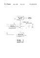
- FIG. 1 is a block diagram for use in schematically describing a conventional transmission power control circuit
- FIG. 2 is a block diagram for use in describing a transmission power control circuit to which this invention is applicable;
- FIG. 3 is a schematic block diagram for use in describing a transmission power control circuit according to a first embodiment of this invention
- FIG. 4 is a specific block diagram of the transmission power control circuit illustrated in FIG. 3;
- FIG. 5 is a partial block diagram for use in describing a transmission power control circuit according to a second embodiment of this invention.
- FIG. 6 is a block diagram for use in describing a mobile station which includes the transmission power control circuit according to this invention.
- the conventional transmission power control circuit comprises a power amplifier 11 which has an amplifier input terminal and an amplifier output terminal and which includes at least one field effect transistor (FET) (not shown) as an amplifying element.
- FET field effect transistor
- the FET has a drain electrode, a source electrode, and a gate electrode.
- the drain electrode of the FET is connected through a drain bias circuit 12 to a power source (not shown) while the gate electrode of the FET is connected to a gate bias controller 13 which has a gate control terminal 14 given a gate control voltage from a controller (not shown).
- the amplifier input terminal is connected to a variable attenuator 16 through a circuit input terminal 17 to which an input transmission signal is given.
- the input transmission signal is delivered to the power amplifier 11 after it is adjusted in level by the attenuator 16 .
- the power amplifier 12 can be selectively put into an on state or an off state by switching a source voltage sent from the power source by the drain bias circuit 12 connected to the drain electrode of the FET.
- the gate electrode of the FET included in the power amplifier 11 is controlled by the gate bias controller 13 connected to the gate control terminal 14 .
- the gate bias voltage of the gate electrode in the FET is varied in response to the gate control signal to change the output power of an output transmission signal over a predetermined range while the power amplifier 11 is turned on.
- the output transmission signal controlled by the gate bias controller 13 is sent from the power amplifier 11 through an isolator 18 to a circuit output terminal 19 as an output signal OUT.
- the transmission power control circuit illustrated in FIG. 1 is disadvantageous in that restricting the drain current is limited to the predetermined range because the power amplifier 11 must be put into an operated state, even when the power amplifier 11 is operated in the low output state, as mentioned before.
- a transmission power control circuit to which this invention is applicable has a preamplifier 20 located before the power amplifier 11 and an isolator 18 connected to the circuit output terminal 19 like in FIG. 1 .
- the illustrated power amplifier 11 is assumed to have an FET like in FIG. 1 and comprises a drain bias circuit 12 ′ connected to the drain electrode of the FET and a gate bias circuit 21 connected to the gate electrode of the FET.
- the illustrated transmission power control circuit has a first switch 22 between the preamplifier 20 and the power amplifier 11 and a second switch 23 between the power amplifier 11 and the isolator 18 .
- Each of the first and the second switches 22 and 23 has a changeover port a, a first switch port b, and a second switch port c.
- a bypass circuit 24 is connected between the second switch ports c of the first and the second switches 22 and 23 while the first switch ports b of the first and the second switches 22 and 23 are connected to an amplifier input terminal and an amplifier output terminal of the power amplifier 11 .
- Each of the first and the second switches 22 and 23 is switched in response to a control signal Co to selectively connect the changeover port a to the first switch port b or the second switch port c.
- the control signal Co is given from a controller (not shown) to each of the first and the second switches 22 and 23 .
- the transmission power control circuit when the transmission power control circuit is operated at a high power level, the changeover ports of the first and the second switches 22 and 23 are connected to the first switch ports b, as shown in FIG. 2 .
- the preamplifier 20 is connected to the power amplifier through the first switch 22 and the power amplifier 11 is connected to the isolator 18 through the second switch 23 . Therefore, a transmission input signal which is given to the preamplifier 20 is amplified by both the preamplifier 20 and the power amplifier 23 into the output signal of the high power level which is sent through the isolator 18 and the circuit output terminal 19 .
- the illustrated transmission power control circuit when the illustrated transmission power control circuit is operated at a low power level, the first and the second switches 22 and 23 are switched from the first switch ports b to the second switch ports c.
- the preamplifier 20 is connected to the bypass circuit 24 through the first switch 22 and is also connected to the isolator 18 through the second switch 23 .
- an output signal amplified by the preamplifier 20 is given as the output signal OUT through the circuit output terminal 19 without being amplified by the power amplifier 11 .
- This shows that the power amplifier 11 is bypassed by the bypass circuit 24 and may be kept inactive under control of the drain bias circuit 12 ′, like in FIG. 1 .
- the transmission power control circuit indispensably causes a power loss to occur at the second switch 23 when the power amplifier 11 is kept active.
- a transmission power control circuit according to a first embodiment of this invention comprises similar parts designated by like reference numerals and symbols in FIG. 2 . More specifically, the illustrated transmission power control circuit has the circuit input terminal (depicted by IN), the circuit output terminal (depicted by OUT), the preamplifier 20 connected to the circuit input terminal IN, the first switch 22 , the drain bias circuit 12 ′, and the gate bias circuit 21 , like in FIG. 2 .
- the power amplifier 11 , the drain bias circuit 12 ′, and the gate bias circuit 21 may be considered as being equivalent to those illustrated in FIG. 2 and may be collectively called a power amplification circuit 25 .
- the power amplifier 11 has an amplifier input terminal and an amplifier output terminal.
- the power amplifier 11 will be called a first transmission circuit while the amplifier input terminal and the amplifier output terminal may be called a first input terminal and a first output terminal, respectively.
- the bypass circuit 24 will be called a second transmission circuit which has a second input terminal and a second output terminal connected to the first and the second switches 22 and 23 ′ in the illustrated manner.
- the first switch 22 is connected between the preamplifier 20 and the amplifier input terminal or the first input terminal of the power amplifier 11 .
- a circulator 30 is connected between the amplifier output terminal or the first output terminal of the power amplifier 11 and the circuit output terminal OUT.
- the illustrated circulator 30 has a first circulator port a 1 connected to the amplifier output terminal of the power amplifier 11 , a second circulator port b 1 connected to the circuit output terminal OUT, and a third circulator port c 1 connected to a second switch 23 ′ which has a changeover port aa, a first switch port bb, and a second port cc.
- the changeover port aa of the second switch 23 ′ is connected to the third circulator port cl of the circulator 30 while the first port bb of the second switch 23 ′ is connected to a terminator 31 which has an impedance determined in relation to a characteristic impedance of a transmission path including the power amplifier 11 .
- the second port cc of the second switch 23 ′ is connected to the second port c of the first switch 22 through the bypass circuit 24 .
- the first and the second switches 22 and 23 ′ may be collectively referred to as a selection circuit which selectively connects the circuit input terminal IN to the power amplifier 11 and the bypass circuit 24 to selectively supply the electric signal to the circuit output terminal OUT.
- the circulator 30 serves to circulate an electric signal from the third circulator port c 1 to the first circulator port a 1 , from the first circulator port a 1 to the second circulator port b 1 , and from the second circulator port b 1 to the third circulator port c 1 .
- the controller 32 detects that a reception or an input signal has a transmission level higher than a predetermined level. Furthermore, it is assumed that the controller 32 delivers a switch control signal to the first and the second switches 22 and 23 ′ to connect the changeover ports a and aa of the first and the second switches 22 and 23 ′ to the first ports b and bb. Consequently, the first port b of the first switch 22 is connected to the power amplifier 11 while the first port bb of the second switch 23 ′ is connected to the terminator 31 . Under the circumstances, both the drain bias circuit 12 ′ and the gate bias circuit 21 become active and, as a result, the power amplifier 11 is put into the active state.
- the transmission input signal which is given through the circuit input terminal IN is delivered to the preamplifier 20 and is preliminarily amplified into a pre-amplified signal.
- the pre-amplified signal is supplied through the first switch 22 to the power amplification circuit 25 and is amplified into an amplified signal to be sent to the first circulator port a 1 of the circulator 30 .
- the amplified signal supplied to the first circulator port a 1 of the circulator 30 is circulated to the second circulator port b 1 of the circulator 30 and is produced as the output signal through the circuit output terminal OUT.
- the controller 32 Let the controller 32 detect that the reception signal has a level which is not higher than the predetermined level. In this case, both the drain bias circuit 12 ′ and the gate bias circuit 21 are put into inactive states and, as a result, the power amplifier 11 becomes inactive. Furthermore, it is surmised that the controller 32 sends the switch control signal to the first and the second switches 22 and 23 ′ to connect the changeover ports a and aa of the first and the second switches 22 and 23 ′ to the second ports c and cc. Thus, the preamplifier 20 is connected to the circulator 30 through the first switch 22 , the bypass circuit 24 , and the second switch 23 ′.
- the pre-amplified signal which is amplified by the preamplifier 20 is sent to the circulator 30 through the first switch port c of the first switch 22 , the bypass circuit 24 , the second switch port cc, and the changeover port aa, and the third circulator port c 1 of the circulator 30 .
- the pre-amplified signal is supplied to the circulator 30 through the bypass circuit 24 without being amplified by the power amplification circuit 25 and may be called a non-amplified signal.
- the non-amplified signal supplied to the third port c 1 of the circulator 30 is circulated from the third circulator port c 1 to the second circulator port b 1 of the circulator 30 and is threreafter circulated from the first circulator port a 1 to the second circulator port b 1 to be produced as the output signal through the circuit output terminal OUT.
- the power amplification circuit 25 When the non-amplified signal is circulated from the third circulator port c 1 to the first circulator port a 1 , the power amplification circuit 25 is put into the inactive state, as mentioned above. This means that an output impedance of the power amplification circuit 25 is extremely high and a voltage standing wave ratio (VSWR) becomes large at the first circulator port a 1 of the circulator 30 . As a result, the non-amplified signal is substantially subjected to reflection at the first circulator port a 1 of the circulator 30 and is circulated to the second circulator port b 1 of the circulator 30 without being attenuated at the first circulator port a 1 . Therefore, the non-amplified signal is transmitted to the circuit output terminal OUT without any loss.
- VSWR voltage standing wave ratio
- the transmission power control circuit comprises an automatic gain control (AGC) amplifier as the preamplifier 20 .
- the AGC amplifier 20 is controlled by the controller 32 which has a main control circuit 321 formed by a CPU and an output power control circuit 322 connected to the AGC amplifier 20 .
- the illustrated output power control circuit 322 also controls the first and the second switches 22 and 23 ′ and the drain bias circuit 12 ′ under control of the main control circuit 321 .
- the main control circuit 321 is coupled to the drain bias circuit 12 ′ and the gate bias circuit 21 .
- the drain bias circuit 12 ′ includes an AND gate 121 , N-channel MOS FET, P-channel MOS FET, and a pull-up resistor 122 all of which are connected in a manner shown in FIG. 4 .
- the AND gate 121 is connected to both the main control circuit 321 and the output power control circuit 322 which are mentioned before.
- the gate bias circuit 21 illustrated in FIG. 4 comprises a digital-to-analog (D/A) converter 211 , an inverting amplifier 212 , and a negative voltage generating/stabilizing circuit 213 which may be structured by a DC—DC converter.
- D/A converter 211 is connected to the main control circuit 321 while the inverting amplifier 212 is located between the D/A converter 211 and the drain bias circuit 12 ′.
- the DC—DC converter 213 is connected to the power source and is also connected to the inverting amplifier 212 .
- the illustrated inverting amplifier 212 is structured by an operational amplifier.
- the main control circuit 321 sends a logic “ 1 ” signal as a main control signal to the drain bias circuit 12 ′ at the beginning of transmission to turn the same into an on-state on one hand and indicates a transmission level to the output power control circuit 322 on the other hand. Responsive to the transmission level, the output power control circuit 322 compares the transmission level with a threshold level.
- the output power control circuit 322 supplies the AGC amplifier 20 with an AGC voltage which corresponds to the transmission level.
- the main control circuit 321 supplies the D/A converter 211 with a digital data signal representative of the transmission level.
- the digital data signal is converted by the D/A converter 211 into an analog signal corresponding to the transmission level and is sent to the inverting amplifier 212 .
- the inverting amplifier 212 is given a positive source voltage +Vcc and a negative source voltage obtained by adding, to ⁇ Vcc, a negative voltage given by the DC—DC converter 213 . With this structure, a negative output voltage can be generated by the inverting amplifier 212 .
- the output power control circuit 322 detects that the transmission level is lower than the threshold level. Under the circumstances, the output power control circuit 322 delivers the switch control signal to the first and the second switches 22 and 23 ′ to bypass the power amplifier 11 by connecting the first and the second switches 22 and 23 ′ to the bypass circuit 24 . In this event, the output power control circuit 322 sends a logic “ 0 ” signal as an off signal to the drain bias circuit 12 ′. As a result, the AND gate 121 of the drain bias circuit 12 ′ produces the logic “ 0 ” signal to put the drain bias circuit 12 ′ into the inactive state.
- the reception signal is given as a transmission input signal through the circuit input terminal IN and is amplified by the AGC amplifier 20 to the transmission level.
- the amplified signal is thereafter sent through the bypass circuit 24 to the circulator 30 when the output power control circuit 322 detects that the transmission level is lower the threshold level.
- the output power control circuit 322 delivers the first and the second switches 22 and 23 ′ to the switch control signal.
- the power amplifier 11 and the terminator 31 are connected to the AGC amplifier 20 and the circulator 30 through the first and the second switches 22 and 23 ′, respectively.
- the logic “ 1 ” level signal is produced by the AND gate 121 of the drain bias circuit 12 ′.
- the N-channel MOS PET is turned into an on state and the P-channel MOS PET is also turned into an on state.
- the power source is electrically connected to the power amplifier 11 through the P-channel MOS FET to supply the source voltage VDD 1 and VDD 2 to the power amplifier 11 .
- the N-channel MOS FET is put into the off state. Since the gate electrode of the P-channel MOS FET is pulled up by the pull-up resistor 122 , the P-channel MOS FET is also put into the off state. No source voltage is given to the power amplifier 11 .
- the illustrated power amplifier 11 includes first and second FETs 111 and 112 each of which has a drain electrode D, a source electrode S, and a gate electrode G. Both the drain electrodes D of the first and the second FETs 111 and 112 are supplied with source voltages VDD 1 and VDD 2 from the drain bias circuit 12 ′ through coils while both the source electrodes S are grounded.
- the gate electrode G of the first FET 111 is coupled to the first switch 22 while the gate electrode G of the second FET 112 is coupled to the drain electrode D of the first FET 111 .
- the drain electrode of the second FET 112 is coupled to the circulator 30 through a capacitor and the amplifier output terminal.
- the gate bias circuit 21 supplies the gate bias voltage Vg to the gate electrodes of the first and the second FETs 111 and 112 through resistors.
- the gate bias circuit 21 makes it possible to set the gate voltages of the first and the second FETs 111 and 112 into optimum levels in accordance with the transmission level. In other words, the consumption current can be determined by the gate bias circuit 21 very efficiently with linearity kept.
- the transmission power control circuit illustrated in FIG. 4 can supply the pre-amplified signal to the third circulator port c 1 of the circulator 30 through the bypass circuit 24 and the second switch port cc of the second switch 23 ′ when the transmission level is lower than the threshold level, as described before.
- the pre-amplified signal is delivered to the circulator 30 without being amplified by the power amplifier 11 and may be called a non-amplified signal.
- the non-amplified signal is circulated from the third circulator port c 1 to the first circulator port a 1 of the circulator 30 and is totally reflected at the first circulator port a 1 because the power amplifier 11 is put into the inactive state. Subsequently, the reflected signal is sent from the first circulator port a 1 to the second circulator port b 1 of the circulator 30 and is produced as the output transmission signal through the circuit output terminal OUT.
- the illustrated transmission power control circuit can bypass a transmission path including the power amplifier 30 at a low transmission level by using the first and the second switches 22 and 23 ′ to switch the transmission path to another transmission path which includes no power amplifier. While the power amplifier 30 is bypassed by the first and the second switches 22 and 23 ′, the power amplifier 30 is kept in the inactive state or an off state under control of the controller 32 . Such an off state of the power amplifier 30 is helpful to increase the VSWR at the first circulator port a 1 of the circulator 30 at which the power amplifier 11 is connected. Accordingly, it is possible to reduce power consumption at the low transmission level and to avoid attenuation of the non-amplified signal.
- a transmission power control circuit comprises an intermediate circuit 35 between the power amplifier (PA) 11 and the circulator 30 both of which are similar to those illustrated in FIGS. 3 and 4.
- the intermediate circuit 35 may be included in the power amplification circuit and is specified by a diode 40 which has an anode connected to the power amplifier 11 and a cathode connected to the first circulator port a 1 of the circulator 30 .
- the diode 40 is connected in an inverse direction with respect to the circulator 30 .
- the illustrated intermediate circuit 35 has choke coils 351 and 352 connected to the anode and the cathode of the diode 40 , respectively, a capacitor 353 connected between the choke coil 352 and the ground, and a resistor 354 connected to the choke coil 352 in series.
- the diode 40 may be, for example, a PIN diode.
- the first circulator port a 1 of the circulator 30 is substantially put into an open state when the power amplifier 11 is bypassed in the manner mentioned before and is seen from the circulator 30 .
- This structure can completely reflect the non-amplified signal given to the first circulator port a 1 from the third circulator port c 1 .
- the non-amplified signal can be circulated or transmitted from the first circulator port a 1 to the second circulator port b 1 without a substantial loss.
- a mobile station which includes the transmission power control circuit illustrated in FIG. 3 or 4 and which comprises a transmitter section 41 and a receiver section 42 .
- the transmission power control circuit is included in the transmitter section 41 and comprises similar parts designated by like reference numerals and symbols, like in FIG. 3 or 4 . Therefore, description will be mainly made about the receiver section 42 .
- the illustrated receiver section 42 is coupled to an antenna through a duplexer 51 used in common to the transmitter section 41 , a low noise amplifier (LNA) 52 , a band-pass filter 53 , a mixer 54 , another band-pass filter 55 , an AGC amplifier 56 , a demodulator 57 , and a reception signal processor 58 .
- LNA low noise amplifier
- the demodulator 57 is coupled to a synthesizer 59 controlled by the main control circuit 321 and supplies the signal processor 58 with a demodulated signal which includes an in-phase component (I) and a quadrature component (Q).
- the in-phase and the quadrature components (I) and (Q) are processed by the reception signal processor 58 into a sequence of reception decoded signals under control of the main control circuit 321 .
- the main control circuit 321 is coupled to a codec 61 which generates a succession of codes which are used for the CDMA system and makes the signal processor 58 decode the in-phase and the quadrature components (I) and (Q) in to the reception decoded signals by the use of the codes.
- Similar operation is carried out in connection with a control signal sent from a base station (not shown). As a result, the control signal is given to the main control circuit 321 . Supplied with the control signal from the base station, the main control circuit 321 indicates the transmission level of the output power control circuit 322 and supplies the gate bias circuit 21 with the digital signal corresponding to the transmission level.
- a transmission signal generator 63 is also included to generate in-phase and quadrature transmission components (I) and (Q) under control of the main control circuit 321 coupled to the codec 61 .
- the transmission signal is coded by the codec 61 into each of the in-phase and the quadrature transmission components (I) and (Q) which is sent from the transmission signal generator 63 in the form of a sequence of digital signals.
- the in-phase and the quadrature transmission components (I) and (Q) are given to a modulator 64 which is coupled to the synthesizer 59 and which may execute quadrature modulation, such as quadrature phase shift keying, quadrature amplitude modulation, to deliver the transmission signal to the AGC amplifier 20 through a band-pass filter 65 .
- quadrature modulation such as quadrature phase shift keying, quadrature amplitude modulation
- the AGC amplifier 20 produces the pre-amplified signal in the manner mentioned in conjunction with FIG. 4 .
- the pre-amplified signal is selectively supplied through the power amplifier 11 to the circulator 30 or through the bypass circuit 24 to the circulator 30 , as mentioned before.
- the pre-amplified signal is directly transmitted through the antenna without being amplified by the power amplifier 11 when the power amplifier 11 is bypassed.
- the illustrated power amplifier 11 itself can also vary output power over a wide range by controlling the drain bias circuit 12 ′ and the gate bias circuit 21 . Accordingly, the transmitter section 41 illustrated in FIG. 6 can control the transmission power over a very wide range. In any event, a transmission output signal is transmitted to the base station in the form of a radio signal through the circulator 30 , the duplexer 51 , and the antenna.
- the synthesizer 59 serves to deliver a local oscillation signal and any other oscillation signals to the mixer 54 , the demodulator 57 , and the modulator 64 .
- the power amplifier 11 may not always have an infinite output impedance when it is bypassed by the bypass circuit 24 but may have a finite output impedance.
- a phase of the pre-amplified signal can be controlled at the first circulator port a 1 of the circulator 30 by using the reflection from the power amplifier 11 .
- the illustrated bypass circuit 24 has been specified by a short-circuit, it may have any impedance.
- the transmission power control circuit according to this invention may be used in a base station.
- the transmission power control circuit according to this invention is advantageous in that current consumption can be remarkably reduced in the transmitter or the transmitter section on low output transmission because no current is substantially caused to flow through the power amplifier 11 . This brings about improvement of efficiency in the transmitter or the transmitter section. Moreover, high power transmission can be carried out like in the conventional circuit by putting the power amplifier 11 into the active state together with the drain bias circuit 12 ′ and the gate bias circuit 21 .
Landscapes
- Engineering & Computer Science (AREA)
- Power Engineering (AREA)
- Transmitters (AREA)
- Amplifiers (AREA)
Abstract
Description
Claims (23)
Applications Claiming Priority (2)
| Application Number | Priority Date | Filing Date | Title |
|---|---|---|---|
| JP10-188738 | 1998-07-03 | ||
| JP10188738A JP2000022559A (en) | 1998-07-03 | 1998-07-03 | Transmission output control circuit |
Publications (1)
| Publication Number | Publication Date |
|---|---|
| US6169449B1 true US6169449B1 (en) | 2001-01-02 |
Family
ID=16228916
Family Applications (1)
| Application Number | Title | Priority Date | Filing Date |
|---|---|---|---|
| US09/345,030 Expired - Lifetime US6169449B1 (en) | 1998-07-03 | 1999-07-02 | Transmission power control circuit capable of varying electric power over a wide range |
Country Status (3)
| Country | Link |
|---|---|
| US (1) | US6169449B1 (en) |
| JP (1) | JP2000022559A (en) |
| GB (1) | GB2339093B (en) |
Cited By (24)
| Publication number | Priority date | Publication date | Assignee | Title |
|---|---|---|---|---|
| US6374127B1 (en) * | 1998-03-05 | 2002-04-16 | Samsung Electronics Co., Ltd. | Power supply apparatus and method for controlling same in a mobile communication terminal |
| US20020072339A1 (en) * | 2000-09-12 | 2002-06-13 | Miikka Hamalainen | Transmitter and wireless communication device |
| EP1370008A1 (en) * | 2002-06-07 | 2003-12-10 | Sony United Kingdom Limited | Mobile transceiver front-end |
| EP1467481A1 (en) * | 2003-04-09 | 2004-10-13 | Sony Ericsson Mobile Communications AB | Glitch-free controllable RF power amplifier |
| US20040252773A1 (en) * | 2003-06-16 | 2004-12-16 | Nati Dinur | Power amplifier pre-distortion device and method for orthogonal frequency division multiplexing |
| US20050090210A1 (en) * | 2002-04-11 | 2005-04-28 | Mitsubishi Denki Kabushiki Kaisha | Communication apparatus |
| US20050136854A1 (en) * | 2003-12-04 | 2005-06-23 | Matsushita Electric Industrial Co., Ltd. | Transmitter |
| US20050136846A1 (en) * | 2003-12-23 | 2005-06-23 | Samsung Electronics Co., Ltd. | RF transceiver |
| US20050174170A1 (en) * | 2001-07-12 | 2005-08-11 | Joachim Herold | Amplifier switch |
| US20060006935A1 (en) * | 2004-06-21 | 2006-01-12 | Samsung Electronics Co., Ltd. | Amplifier |
| US20060126864A1 (en) * | 2002-09-11 | 2006-06-15 | Dmb Technology Co., Ltd. | Circuit and method for eliminating pop noise in digital audio amplifier using dual power supply |
| US20060244538A1 (en) * | 2004-03-23 | 2006-11-02 | Sadao Yamashita | Fet amplifier, pulse modulation module, and radar device |
| US7184799B1 (en) * | 2003-05-14 | 2007-02-27 | Marvell International Ltd. | Method and apparatus for reducing wake up time of a powered down device |
| US20070211820A1 (en) * | 2005-02-03 | 2007-09-13 | Yoshihiro Hara | Transmission Device And Wireless Communication Apparatus |
| US20080026710A1 (en) * | 2006-07-27 | 2008-01-31 | Harris Corporation | Power management scheme for software-defined radios |
| KR100876937B1 (en) * | 2007-05-07 | 2009-01-09 | 주식회사 에이스테크놀로지 | Tower-top low noise amplifier in time division duplexing communication system |
| US20090251209A1 (en) * | 2008-04-03 | 2009-10-08 | Mitsubishi Electric Corporation | High frequency power amplifier |
| US20110021237A1 (en) * | 2008-02-08 | 2011-01-27 | Skyworks Solutions, Inc. | Closed-Loop Adaptive Power Control For Adjusting Bandwidth In A Mobile Handset Transmitter |
| US8095091B1 (en) * | 2007-05-18 | 2012-01-10 | Marvell International Ltd. | Transmit power amplification control for wireless device |
| US20130070749A1 (en) * | 2011-09-20 | 2013-03-21 | Avago Technologies Wireless Ip (Singapore) Pte. Ltd. | Device for separating signal transmission and reception and communication system including same |
| GB2495605A (en) * | 2011-10-11 | 2013-04-17 | Furuno Electric Co | A pulsed radar transmitter amplifier with rapid turn-off |
| TWI456893B (en) * | 2005-11-01 | 2014-10-11 | Diodes Taiwan Inc | Monolithic integrated circuit with voltage regulator circuit and negative voltage generator circuit and low noise amplifier |
| US9294143B1 (en) * | 2014-06-13 | 2016-03-22 | L-3 Communications Corp. | Circulator used as a high power TX/RX switch |
| US9596649B1 (en) | 2007-05-18 | 2017-03-14 | Marvell International Ltd. | Power saving technique for a wireless device |
Families Citing this family (8)
| Publication number | Priority date | Publication date | Assignee | Title |
|---|---|---|---|---|
| US6060949A (en) * | 1998-09-22 | 2000-05-09 | Qualcomm Incorporated | High efficiency switched gain power amplifier |
| US6806768B2 (en) * | 2001-10-31 | 2004-10-19 | Qualcomm Incorporated | Balanced power amplifier with a bypass structure |
| CN100407582C (en) * | 2004-09-07 | 2008-07-30 | 华为技术有限公司 | Manual apparatus for delaying work time and realization thereof |
| JP5086524B2 (en) * | 2005-01-13 | 2012-11-28 | ルネサスエレクトロニクス株式会社 | Controller / driver and liquid crystal display device using the same |
| US8812052B2 (en) | 2007-02-27 | 2014-08-19 | Qualcomm Incorporated | SPS receiver with adjustable linearity |
| US9231630B2 (en) | 2009-05-05 | 2016-01-05 | San Diego, CA | Radio device having dynamic intermediate frequency scaling |
| KR101067112B1 (en) | 2009-06-08 | 2011-09-22 | 삼성전기주식회사 | Low Noise Amplifier |
| CN104158505A (en) * | 2013-05-14 | 2014-11-19 | 中兴通讯股份有限公司 | Radio frequency power amplification circuit, control method and terminal |
Citations (9)
| Publication number | Priority date | Publication date | Assignee | Title |
|---|---|---|---|---|
| US3992669A (en) | 1975-08-29 | 1976-11-16 | Gte Automatic Electric Laboratories Incorporated | Radio frequency protection circuit |
| US4056785A (en) | 1976-12-06 | 1977-11-01 | Bell Telephone Laboratories, Incorporated | Low-noise microwave amplifier |
| US4305043A (en) | 1980-03-03 | 1981-12-08 | Ford Aerospace & Communications Corporation | Coupler having arbitrary impedance transformation ratio and arbitrary coubling ratio |
| US4910478A (en) | 1988-06-10 | 1990-03-20 | Mitsubishi Denki Kabushiki Kaisha | Amplifier circuit and method of controlling output power thereof |
| JPH0583041A (en) | 1990-11-30 | 1993-04-02 | Nec Corp | Gate bias control circuit |
| JPH07336243A (en) | 1994-06-10 | 1995-12-22 | Matsushita Electric Ind Co Ltd | Transmission output controller |
| JPH08222963A (en) | 1995-02-10 | 1996-08-30 | Sanyo Electric Co Ltd | Transmission power control circuit |
| EP0735668A1 (en) | 1995-03-30 | 1996-10-02 | AT&T IPM Corp. | High-efficient configurable power amplifier for use in a portable unit |
| US5909643A (en) * | 1995-11-24 | 1999-06-01 | Matsushita Electric Industrial Co., Ltd. | Transmitter power varying device having a bypass line for a power amplifier |
-
1998
- 1998-07-03 JP JP10188738A patent/JP2000022559A/en active Pending
-
1999
- 1999-07-02 US US09/345,030 patent/US6169449B1/en not_active Expired - Lifetime
- 1999-07-05 GB GB9915704A patent/GB2339093B/en not_active Expired - Fee Related
Patent Citations (9)
| Publication number | Priority date | Publication date | Assignee | Title |
|---|---|---|---|---|
| US3992669A (en) | 1975-08-29 | 1976-11-16 | Gte Automatic Electric Laboratories Incorporated | Radio frequency protection circuit |
| US4056785A (en) | 1976-12-06 | 1977-11-01 | Bell Telephone Laboratories, Incorporated | Low-noise microwave amplifier |
| US4305043A (en) | 1980-03-03 | 1981-12-08 | Ford Aerospace & Communications Corporation | Coupler having arbitrary impedance transformation ratio and arbitrary coubling ratio |
| US4910478A (en) | 1988-06-10 | 1990-03-20 | Mitsubishi Denki Kabushiki Kaisha | Amplifier circuit and method of controlling output power thereof |
| JPH0583041A (en) | 1990-11-30 | 1993-04-02 | Nec Corp | Gate bias control circuit |
| JPH07336243A (en) | 1994-06-10 | 1995-12-22 | Matsushita Electric Ind Co Ltd | Transmission output controller |
| JPH08222963A (en) | 1995-02-10 | 1996-08-30 | Sanyo Electric Co Ltd | Transmission power control circuit |
| EP0735668A1 (en) | 1995-03-30 | 1996-10-02 | AT&T IPM Corp. | High-efficient configurable power amplifier for use in a portable unit |
| US5909643A (en) * | 1995-11-24 | 1999-06-01 | Matsushita Electric Industrial Co., Ltd. | Transmitter power varying device having a bypass line for a power amplifier |
Cited By (45)
| Publication number | Priority date | Publication date | Assignee | Title |
|---|---|---|---|---|
| US6374127B1 (en) * | 1998-03-05 | 2002-04-16 | Samsung Electronics Co., Ltd. | Power supply apparatus and method for controlling same in a mobile communication terminal |
| US20020072339A1 (en) * | 2000-09-12 | 2002-06-13 | Miikka Hamalainen | Transmitter and wireless communication device |
| US6954624B2 (en) * | 2000-09-12 | 2005-10-11 | Nokia Mobile Phones Ltd. | Transmitter and wireless communication device having a low power bypass branch |
| US20050174170A1 (en) * | 2001-07-12 | 2005-08-11 | Joachim Herold | Amplifier switch |
| US7064604B2 (en) * | 2001-07-12 | 2006-06-20 | Kathrein-Werke Kg | Amplifier switch |
| US20050090210A1 (en) * | 2002-04-11 | 2005-04-28 | Mitsubishi Denki Kabushiki Kaisha | Communication apparatus |
| EP1370008A1 (en) * | 2002-06-07 | 2003-12-10 | Sony United Kingdom Limited | Mobile transceiver front-end |
| US7313244B2 (en) * | 2002-09-11 | 2007-12-25 | Dmb Technology Co., Ltd. | Circuit and method for eliminating pop noise in digital audio amplifier using dual power supply |
| US20060126864A1 (en) * | 2002-09-11 | 2006-06-15 | Dmb Technology Co., Ltd. | Circuit and method for eliminating pop noise in digital audio amplifier using dual power supply |
| EP1467481A1 (en) * | 2003-04-09 | 2004-10-13 | Sony Ericsson Mobile Communications AB | Glitch-free controllable RF power amplifier |
| US7365599B2 (en) | 2003-04-09 | 2008-04-29 | Sony Ericsson Mobile Communications Ab | Glitch-free controllable RF power amplifier |
| US7184799B1 (en) * | 2003-05-14 | 2007-02-27 | Marvell International Ltd. | Method and apparatus for reducing wake up time of a powered down device |
| US8781539B1 (en) | 2003-05-14 | 2014-07-15 | Marvell International Ltd. | Method and apparatus for reducing wake up time of a powered down device |
| US8359074B1 (en) | 2003-05-14 | 2013-01-22 | Marvell International Ltd. | Method and apparatus for reducing wake up time of a powered down device |
| US20040252773A1 (en) * | 2003-06-16 | 2004-12-16 | Nati Dinur | Power amplifier pre-distortion device and method for orthogonal frequency division multiplexing |
| US7310381B2 (en) * | 2003-06-16 | 2007-12-18 | Intel Corporation | Power amplifier pre-distortion device and method for orthogonal frequency division multiplexing |
| US20050136854A1 (en) * | 2003-12-04 | 2005-06-23 | Matsushita Electric Industrial Co., Ltd. | Transmitter |
| US20050136846A1 (en) * | 2003-12-23 | 2005-06-23 | Samsung Electronics Co., Ltd. | RF transceiver |
| US20060244538A1 (en) * | 2004-03-23 | 2006-11-02 | Sadao Yamashita | Fet amplifier, pulse modulation module, and radar device |
| US7365603B2 (en) * | 2004-03-23 | 2008-04-29 | Murata Manufacturing Co., Ltd. | FET amplifier, pulse modulation module, and radar device |
| US7292096B2 (en) * | 2004-06-21 | 2007-11-06 | Samsung Electronics Co., Ltd. | Amplifier |
| US20060006935A1 (en) * | 2004-06-21 | 2006-01-12 | Samsung Electronics Co., Ltd. | Amplifier |
| US20070211820A1 (en) * | 2005-02-03 | 2007-09-13 | Yoshihiro Hara | Transmission Device And Wireless Communication Apparatus |
| US7664202B2 (en) * | 2005-02-03 | 2010-02-16 | Panasonic Corporation | Transmission device and wireless communication apparatus |
| TWI456893B (en) * | 2005-11-01 | 2014-10-11 | Diodes Taiwan Inc | Monolithic integrated circuit with voltage regulator circuit and negative voltage generator circuit and low noise amplifier |
| US20080026710A1 (en) * | 2006-07-27 | 2008-01-31 | Harris Corporation | Power management scheme for software-defined radios |
| US7590395B2 (en) * | 2006-07-27 | 2009-09-15 | Harris Corporation | Power management scheme for software-defined radios |
| KR100876937B1 (en) * | 2007-05-07 | 2009-01-09 | 주식회사 에이스테크놀로지 | Tower-top low noise amplifier in time division duplexing communication system |
| US20120115538A1 (en) * | 2007-05-18 | 2012-05-10 | Marvell Semiconductor, Inc. | Transmit power amplification control for wireless device |
| US8095091B1 (en) * | 2007-05-18 | 2012-01-10 | Marvell International Ltd. | Transmit power amplification control for wireless device |
| US9596649B1 (en) | 2007-05-18 | 2017-03-14 | Marvell International Ltd. | Power saving technique for a wireless device |
| US8538356B2 (en) * | 2007-05-18 | 2013-09-17 | Marvell International Ltd. | Transmit power amplification control for wireless device |
| US8798562B2 (en) | 2007-05-18 | 2014-08-05 | Marvell International Ltd. | Transmit power amplification control for wireless device |
| US20110021237A1 (en) * | 2008-02-08 | 2011-01-27 | Skyworks Solutions, Inc. | Closed-Loop Adaptive Power Control For Adjusting Bandwidth In A Mobile Handset Transmitter |
| US8606311B2 (en) * | 2008-02-08 | 2013-12-10 | Skyworks Solutions, Inc. | Closed-loop adaptive power control for adjusting bandwidth in a mobile handset transmitter |
| US7679441B2 (en) | 2008-04-03 | 2010-03-16 | Mitsubishi Electric Corporation | High frequency power amplifier |
| US20090251209A1 (en) * | 2008-04-03 | 2009-10-08 | Mitsubishi Electric Corporation | High frequency power amplifier |
| US8908668B2 (en) * | 2011-09-20 | 2014-12-09 | Avago Technologies General Ip (Singapore) Pte. Ltd. | Device for separating signal transmission and reception and communication system including same |
| US20130070749A1 (en) * | 2011-09-20 | 2013-03-21 | Avago Technologies Wireless Ip (Singapore) Pte. Ltd. | Device for separating signal transmission and reception and communication system including same |
| GB2495605A (en) * | 2011-10-11 | 2013-04-17 | Furuno Electric Co | A pulsed radar transmitter amplifier with rapid turn-off |
| US8994579B2 (en) | 2011-10-11 | 2015-03-31 | Furuno Electric Company Ltd. | RF pulse signal generation switching circuit, RF pulse signal generating circuit, and target object detecting apparatus |
| CN103051328A (en) * | 2011-10-11 | 2013-04-17 | 古野电气株式会社 | RF pulse signal generation switching circuit, RF pulse signal generating circuit, and target object detecting apparatus |
| CN103051328B (en) * | 2011-10-11 | 2017-04-12 | 古野电气株式会社 | RF pulse signal generation switching circuit, RF pulse signal generating circuit, and target object detecting apparatus |
| GB2495605B (en) * | 2011-10-11 | 2018-08-08 | Furuno Electric Co | RF pulse signal generation switching circuit, RF pulse signal generating circuit, and target object detecting apparatus |
| US9294143B1 (en) * | 2014-06-13 | 2016-03-22 | L-3 Communications Corp. | Circulator used as a high power TX/RX switch |
Also Published As
| Publication number | Publication date |
|---|---|
| JP2000022559A (en) | 2000-01-21 |
| GB2339093A (en) | 2000-01-12 |
| GB9915704D0 (en) | 1999-09-08 |
| GB2339093B (en) | 2003-03-12 |
Similar Documents
| Publication | Publication Date | Title |
|---|---|---|
| US6169449B1 (en) | Transmission power control circuit capable of varying electric power over a wide range | |
| US6215987B1 (en) | Mobile communication transmitter capable of selectively activating amplifiers | |
| US7336127B2 (en) | Doherty amplifier configuration for a collector controlled power amplifier | |
| EP0977354B1 (en) | Amplifier for radio transmission | |
| US5541554A (en) | Multi-mode power amplifier | |
| EP1127406B1 (en) | High efficiency power amplifier | |
| CA2075588C (en) | Power amplifier for a cellular telephone | |
| US20030222709A1 (en) | High efficiency power amplifier | |
| US6201441B1 (en) | Semiconductor circuit | |
| US6359514B1 (en) | Switchable path power amplifier with combining network | |
| KR100422894B1 (en) | Low-noise amplifier with switched gain and method | |
| JPH077449A (en) | Antenna change-over switch | |
| US6342812B1 (en) | Power amplification system for low power radio frequency signals | |
| EP0874452B1 (en) | Reception circuit for cellular telephone | |
| US5995853A (en) | Power control technique of radio communication system | |
| EP1012993B1 (en) | A radio front-end circuit | |
| US6711392B1 (en) | Balanced power amplifier for low power radio communications | |
| US6445729B1 (en) | Radio signal transceiver apparatus | |
| JP2000165311A (en) | Output circuit for portable terminal | |
| KR100950618B1 (en) | A linear power efficient radio frequencyrf driver system and method with power level control | |
| US7190228B2 (en) | Gain control device of transmitter in mobile communication terminal and method thereof | |
| JP2000349657A (en) | Rf detection circuit | |
| JPH11145748A (en) | Power amplifier circuit | |
| KR20040095286A (en) | Front stage amplifier with different modes | |
| JP2003017957A (en) | High frequency amplifier and receiver employing the same |
Legal Events
| Date | Code | Title | Description |
|---|---|---|---|
| AS | Assignment |
Owner name: NEC CORPORATION, JAPAN Free format text: ASSIGNMENT OF ASSIGNORS INTEREST;ASSIGNOR:HASEGAWA, OSAMU;REEL/FRAME:010094/0733 Effective date: 19990629 |
|
| FEPP | Fee payment procedure |
Free format text: PAYOR NUMBER ASSIGNED (ORIGINAL EVENT CODE: ASPN); ENTITY STATUS OF PATENT OWNER: LARGE ENTITY |
|
| STCF | Information on status: patent grant |
Free format text: PATENTED CASE |
|
| CC | Certificate of correction | ||
| FPAY | Fee payment |
Year of fee payment: 4 |
|
| FPAY | Fee payment |
Year of fee payment: 8 |
|
| FPAY | Fee payment |
Year of fee payment: 12 |
|
| AS | Assignment |
Owner name: WARREN & LEWIS INVESTMENT CORPORATION, VIRGINIA Free format text: ASSIGNMENT OF ASSIGNORS INTEREST;ASSIGNOR:NEC CORPORATION;REEL/FRAME:029216/0855 Effective date: 20120903 |
|
| AS | Assignment |
Owner name: NEC CORPORATION, JAPAN Free format text: NOTICE OF TERMINATION;ASSIGNOR:WARREN & LEWIS INVESTMENT CORPORATION;REEL/FRAME:034244/0623 Effective date: 20141113 |
|
| AS | Assignment |
Owner name: NEC CORPORATION, JAPAN Free format text: NUNC PRO TUNC ASSIGNMENT;ASSIGNORS:WARREN & LEWIS INVESTMENT CORPORATION;COMMIX SYSTEMS, LCC;REEL/FRAME:037209/0592 Effective date: 20151019 |
|
| AS | Assignment |
Owner name: NEC CORPORATION, JAPAN Free format text: CORRECTIVE ASSIGNMENT TO CORRECT THE SECOND CONVEYING PARTY NAME PREVIOUSLY RECORDED AT REEL: 037209 FRAME: 0592. ASSIGNOR(S) HEREBY CONFIRMS THE ASSIGNMENT;ASSIGNORS:WARREN & LEWIS INVESTMENT CORPORATION;COMMIX SYSTEMS, LLC;REEL/FRAME:037279/0685 Effective date: 20151019 |