US6166529A - Voltage-current conversion circuit - Google Patents
Voltage-current conversion circuit Download PDFInfo
- Publication number
- US6166529A US6166529A US09/511,935 US51193500A US6166529A US 6166529 A US6166529 A US 6166529A US 51193500 A US51193500 A US 51193500A US 6166529 A US6166529 A US 6166529A
- Authority
- US
- United States
- Prior art keywords
- current
- transistors
- mirror circuit
- voltage
- circuit
- Prior art date
- Legal status (The legal status is an assumption and is not a legal conclusion. Google has not performed a legal analysis and makes no representation as to the accuracy of the status listed.)
- Expired - Lifetime
Links
Images

Classifications
-
- G—PHYSICS
- G05—CONTROLLING; REGULATING
- G05F—SYSTEMS FOR REGULATING ELECTRIC OR MAGNETIC VARIABLES
- G05F1/00—Automatic systems in which deviations of an electric quantity from one or more predetermined values are detected at the output of the system and fed back to a device within the system to restore the detected quantity to its predetermined value or values, i.e. retroactive systems
- G05F1/10—Regulating voltage or current
- G05F1/46—Regulating voltage or current wherein the variable actually regulated by the final control device is dc
- G05F1/56—Regulating voltage or current wherein the variable actually regulated by the final control device is dc using semiconductor devices in series with the load as final control devices
- G05F1/561—Voltage to current converters
-
- G—PHYSICS
- G05—CONTROLLING; REGULATING
- G05F—SYSTEMS FOR REGULATING ELECTRIC OR MAGNETIC VARIABLES
- G05F3/00—Non-retroactive systems for regulating electric variables by using an uncontrolled element, or an uncontrolled combination of elements, such element or such combination having self-regulating properties
- G05F3/02—Regulating voltage or current
- G05F3/08—Regulating voltage or current wherein the variable is dc
- G05F3/10—Regulating voltage or current wherein the variable is dc using uncontrolled devices with non-linear characteristics
- G05F3/16—Regulating voltage or current wherein the variable is dc using uncontrolled devices with non-linear characteristics being semiconductor devices
- G05F3/20—Regulating voltage or current wherein the variable is dc using uncontrolled devices with non-linear characteristics being semiconductor devices using diode- transistor combinations
- G05F3/24—Regulating voltage or current wherein the variable is dc using uncontrolled devices with non-linear characteristics being semiconductor devices using diode- transistor combinations wherein the transistors are of the field-effect type only
- G05F3/242—Regulating voltage or current wherein the variable is dc using uncontrolled devices with non-linear characteristics being semiconductor devices using diode- transistor combinations wherein the transistors are of the field-effect type only with compensation for device parameters, e.g. channel width modulation, threshold voltage, processing, or external variations, e.g. temperature, loading, supply voltage
Definitions
- the present invention relates generally to a voltage-current conversion circuit, and more particularly, a voltage-current conversion circuit outputting a current corresponding to a difference in input voltages applied to a pair of transistors forming a differential circuit.
- FIG. 1 input voltages Vin1, Vin2 are applied to a pair of input terminals 10, 11.
- Each of the input terminals 10, 11 is connected to the bases of npn transistors Q1, Q2, respectively, the npn transistors Q1, Q2 forming a differential circuit.
- the collectors of transistors Q1, Q2 are connected to the collectors of transistors Q3, Q4.
- Transistors Q3, Q4 form a current-mirror circuit, their bases being connected to each other and jointly connected to the collector of Q3 and their respective emitters being connected to a power source Vcc.
- An output terminal 14 outputting a current Iout is connected to the collector of the transistor Q4.
- the emitters of transistors Q1, Q2 are connected both to the two ends of the resistor Rg as well as to a constant current source 12, 13 generating constant currents I, I' (I' ⁇ I).
- a requirement of the conventional circuit described above is that the input voltages Vin1, Vin2 be lower than the power source voltage Vcc. If this requirement is not met the circuit does not operate properly. As a result, the size of the input voltages Vin1, Vin2 is limited and hence the range of applications of the circuit is limited as well.
- a more specific object of the present invention is to provide an improved and useful voltage-current conversion circuit not restricted by the requirement that the input voltages be lower than the power source voltage and hence capable of an expanded range of applications.
- a voltage-current conversion circuit outputting a current corresponding to a difference between a first input voltage and a second input voltage
- the voltage-current conversion circuit comprising:
- a first current-mirror circuit supplied with the first input voltage as a power source and comprising at least one pair of transistors;
- a second current-mirror circuit supplied with the second input voltage as a power source and comprising at least one pair of transistors;
- a third current-mirror circuit comprising:
- a current output terminal being connected to one of the current source transistors.
- the voltage-current conversion circuit not restricted by the requirement that the input voltages be lower than the power source voltage because the first and second input voltages are supplied to the first and second current-mirror circuits as power sources.
- the voltage-current conversion circuit is capable of an expanded range of applications.
- the above-described object of the present invention is also achieved by the voltage-current conversion circuit as described above, wherein the first current-mirror circuit and the second current-mirror circuit are Wilson-type current-mirror circuits.
- the identity of the current flowing to the pairs of transistors forming the first and second current-mirror circuits increases.
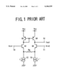
- FIG. 1 shows a conventional voltage-current conversion-circuit
- FIG. 2 shows an embodiment of a voltage-current conversion circuit according to the present invention.
- FIG. 2 shows an embodiment of a voltage-current conversion circuit according to the present invention.
- input voltages Vin1, Vin2 are applied to a pair of input terminals 20, 21, respectively.
- Input terminal 20 is connected to the emitters of pnp transistors Q11, Q12 which together form a current mirror circuit.
- Input terminal 21 is connected to the emitters of pnp transistors Q21, Q22 which together form a current-mirror circuit.
- the bases of transistors Q11, Q12 are connected to each other and jointly connected to the collector of transistor Q12.
- the collectors of transistors Q11, Q12 are connected to the emitters of pnp transistors Q13, Q14.
- the bases of transistors Q13, Q14 are connected to each other and jointly connected to the collector of transistor Q13 to form a current-mirror circuit.
- Transistors Q11, Q12, together with transistors Q13, Q14, form a Wilson-type current-mirror circuit.
- the collector of transistor Q13 is grounded via a constant current source 22 that generates a constant current I.
- the collector of transistor Q14 is connected to the collector of npn transistor Q15.
- the bases of transistors Q21, Q22 are connected to each other and jointly connected to the collector of transistor Q22.
- the collectors of transistors Q21, Q22 are connected to the emitters of pnp transistors Q23, Q24.
- the bases of transistors Q23, Q24 are collected to each other and jointly connected to the collector of transistor Q23 to form a current-mirror circuit.
- the collector of transistor Q23 is grounded via a constant current source 23 that generates a constant current I.
- a resistor Rg is connected between the collector of transistor Q12 and the collector of transistor Q22. Additionally, the base of transistor Q15 is connected to the collector of transistor Q15, the base of transistor Q15 is connected to the base of transistor Q25 and the emitters of transistors Q15, Q25 are grounded to form a current-mirror circuit. Additionally, an output terminal 24 is connected to the collector of transistor Q25. Power for the entire circuit is supplied from input voltages Vin1, Vin2.
- Transistors Q13, Q14 act to correct the base current of transistors Q11, Q12 and eliminate the early effect of transistors Q11, Q12, thus increasing the identity of the emitter current of transistors Q11, Q12.
- constant current sources 22, 23 generate the same constant current I
- transistors Q15, Q25 form a current-mirror circuit and the respective emitter currents are approximately identical, that is, equal to I, so the emitter currents of transistors Q11, Q12, Q21, Q22 become identical.
- a current Iout corresponding to the difference between input voltages Vin1 and Vin2 (Vin1-Vin2) is output from output terminal 24.
- the power for the circuit is supplied from the input voltages Vin1, Vin2 and no conditions restrict input voltages Vin1, Vin2, so the circuit can be used in an expanded range of applications as compared to the conventional art.
- pnp transistors and npn transistors may be replaced with npn transistors and pnp transistors, respectively, and moreover a negative power source may be used instead of the ground level so as to accommodate input voltages Vin1, Vin2 less than that of the ground level.
- circuit according to the embodiment described above can also be used in conjunction with a circuit in which the pnp transistors and npn transistors are switched as described above and the input terminal switched so as to be connected to one or the other circuit depending on whether the input voltages Vin1, Vin2 are greater than ground level or less than ground level.
- transistors Q11, Q12, Q13, Q14 correspond to the first current-mirror circuit claimed hereinbelow
- transistors Q21, Q22, Q23, Q24 correspond to the second current-mirror circuit claimed hereinbelow
- transistors Q15, Q25 correspond to the third current-mirror circuit as claimed hereinbelow.
Landscapes
- Engineering & Computer Science (AREA)
- Physics & Mathematics (AREA)
- Electromagnetism (AREA)
- General Physics & Mathematics (AREA)
- Radar, Positioning & Navigation (AREA)
- Automation & Control Theory (AREA)
- Amplifiers (AREA)
Abstract
A voltage-current conversion circuit outputting a current corresponding to a difference between a first input voltage and a second input voltage, the voltage-current conversion circuit having a first current-mirror circuit supplied with the first input voltage as a power source and comprising at least one pair of transistors, a second current-mirror circuit supplied with the second input voltage as a power source and comprising at least one pair of transistors, a resistor connected between one of the pair of transistors of the first current-mirror circuit and one of the transistors of the second current-mirror circuit, and a third current-mirror circuit having a current source transistor supplying current to one of the pair of transistors of the first current-mirror circuit and another current source transistor supplying current to one of the pair of transistors of the second current-mirror circuit, a current output terminal being connected to one of the current source transistors.
Description
1. Field of the Invention
The present invention relates generally to a voltage-current conversion circuit, and more particularly, a voltage-current conversion circuit outputting a current corresponding to a difference in input voltages applied to a pair of transistors forming a differential circuit.
2. Description of the Related Art
Conventionally, as a voltage-current conversion circuit adapted for a variable low-pass filter, electronic volume and the like, a circuit like that shown in FIG. 1 is known. In FIG. 1, input voltages Vin1, Vin2 are applied to a pair of input terminals 10, 11. Each of the input terminals 10, 11 is connected to the bases of npn transistors Q1, Q2, respectively, the npn transistors Q1, Q2 forming a differential circuit. The collectors of transistors Q1, Q2 are connected to the collectors of transistors Q3, Q4. Transistors Q3, Q4 form a current-mirror circuit, their bases being connected to each other and jointly connected to the collector of Q3 and their respective emitters being connected to a power source Vcc.
An output terminal 14 outputting a current Iout is connected to the collector of the transistor Q4. The emitters of transistors Q1, Q2 are connected both to the two ends of the resistor Rg as well as to a constant current source 12, 13 generating constant currents I, I' (I'≈I).
It should be noted that when an input voltage differential dV (=Vin1 minus Vin2) is applied between the input terminals 10, 11 a current Ig (=dV/Rg) corresponding to the voltage dV flows to the resistor Rg, the output current Iout being generated based on the current Ig.
A requirement of the conventional circuit described above is that the input voltages Vin1, Vin2 be lower than the power source voltage Vcc. If this requirement is not met the circuit does not operate properly. As a result, the size of the input voltages Vin1, Vin2 is limited and hence the range of applications of the circuit is limited as well.
Accordingly, it is a general object of the present invention to provide an improved and useful voltage-current conversion circuit in which the disadvantages described above are eliminated.
A more specific object of the present invention is to provide an improved and useful voltage-current conversion circuit not restricted by the requirement that the input voltages be lower than the power source voltage and hence capable of an expanded range of applications.
The above-described object of the present invention is achieved by a voltage-current conversion circuit outputting a current corresponding to a difference between a first input voltage and a second input voltage, the voltage-current conversion circuit comprising:
a first current-mirror circuit supplied with the first input voltage as a power source and comprising at least one pair of transistors;
a second current-mirror circuit supplied with the second input voltage as a power source and comprising at least one pair of transistors;
a resistor connected between one of the pair of transistors of the first current-mirror circuit and one of the transistors of the second current-mirror circuit; and
a third current-mirror circuit comprising:
a current source transistor supplying current to one of the pair of transistors of the first current-mirror circuit; and
another current source transistor supplying current to one of the pair of transistors of the second current-mirror circuit,
a current output terminal being connected to one of the current source transistors.
According to the invention described above, the voltage-current conversion circuit not restricted by the requirement that the input voltages be lower than the power source voltage because the first and second input voltages are supplied to the first and second current-mirror circuits as power sources. As a result, the voltage-current conversion circuit is capable of an expanded range of applications.
Additionally, the above-described object of the present invention is also achieved by the voltage-current conversion circuit as described above, wherein the first current-mirror circuit and the second current-mirror circuit are Wilson-type current-mirror circuits.
According to the invention described above, the identity of the current flowing to the pairs of transistors forming the first and second current-mirror circuits increases.
Other objects, features and advantages of the present invention will become more apparent from the following detailed description when read in conjunction with the accompanying drawings.
FIG. 1 shows a conventional voltage-current conversion-circuit; and
FIG. 2 shows an embodiment of a voltage-current conversion circuit according to the present invention.
A description will now be given of a preferred embodiment of a voltage-current conversion circuit according to the present invention, with reference to the accompanying drawings.
FIG. 2 shows an embodiment of a voltage-current conversion circuit according to the present invention. As shown in the diagram, input voltages Vin1, Vin2 are applied to a pair of input terminals 20, 21, respectively. Input terminal 20 is connected to the emitters of pnp transistors Q11, Q12 which together form a current mirror circuit. Input terminal 21 is connected to the emitters of pnp transistors Q21, Q22 which together form a current-mirror circuit.
The bases of transistors Q11, Q12 are connected to each other and jointly connected to the collector of transistor Q12. The collectors of transistors Q11, Q12 are connected to the emitters of pnp transistors Q13, Q14. The bases of transistors Q13, Q14 are connected to each other and jointly connected to the collector of transistor Q13 to form a current-mirror circuit. Transistors Q11, Q12, together with transistors Q13, Q14, form a Wilson-type current-mirror circuit. The collector of transistor Q13 is grounded via a constant current source 22 that generates a constant current I. The collector of transistor Q14 is connected to the collector of npn transistor Q15.
At the same time, the bases of transistors Q21, Q22 are connected to each other and jointly connected to the collector of transistor Q22. The collectors of transistors Q21, Q22 are connected to the emitters of pnp transistors Q23, Q24. The bases of transistors Q23, Q24 are collected to each other and jointly connected to the collector of transistor Q23 to form a current-mirror circuit. Transistors Q21, Q22, together with transistors Q23, Q24, form a Wilson-type current-mirror circuit. The collector of transistor Q23 is grounded via a constant current source 23 that generates a constant current I.
A resistor Rg is connected between the collector of transistor Q12 and the collector of transistor Q22. Additionally, the base of transistor Q15 is connected to the collector of transistor Q15, the base of transistor Q15 is connected to the base of transistor Q25 and the emitters of transistors Q15, Q25 are grounded to form a current-mirror circuit. Additionally, an output terminal 24 is connected to the collector of transistor Q25. Power for the entire circuit is supplied from input voltages Vin1, Vin2.
A description will now be given of the operation of the transistors Q11, Q12, Q13, Q14 that together form the Wilson-type current-mirror circuit. Transistors Q13, Q14 act to correct the base current of transistors Q11, Q12 and eliminate the early effect of transistors Q11, Q12, thus increasing the identity of the emitter current of transistors Q11, Q12.
That is, if a forward voltage drop between the bases and emitters of transistors Q13, Q14 is Vbe13, Vbe14 (Vbe13=Vbe14), then the electric potential at the collector of transistor Q12 can be expressed as -Vbe14+Vbe13=electric potential at the collector of transistor Q11, and the electric potentials at the collectors of transistors Q11, Q12 become identical and, as a result, the respective emitter currents of transistors Q11, Q12 become identical.
Similarly, if a forward voltage drop between the bases and emitters of transistors Q23, Q24 is Vbe23, Vbe24 (Vbe23=Vbe24), then the electric potential at the collector of transistor Q22 can be expressed as -Vbe24+Vbe23=electric potential at the collector of transistor Q21, and the electric potentials at the collectors of transistors Q21, Q22 become identical and, as a result, the respective emitter currents of transistors Q21, Q22 become identical.
Additionally, constant current sources 22, 23 generate the same constant current I, transistors Q15, Q25 form a current-mirror circuit and the respective emitter currents are approximately identical, that is, equal to I, so the emitter currents of transistors Q11, Q12, Q21, Q22 become identical.
If input voltages Vin1, Vin2 are identical, and if a forward voltage drop between the bases and emitters of transistors Q12, Q21 is Vbe12, Vbe22 (Vbe12=Vbe22), then at the collectors of transistors Q12, Q22
Vin1-Vbe12=Vin2-Vbe22
and no current flows to the resistor Rg.
For example, assuming an input voltage Vin2 rises such that Vin1<Vin2, then Vin1-Vbe12<Vin2-Vbe22 and a current Ir [Ir=(Vin2-Vin1)] flows from transistor Q22 toward transistor Q12 to resistor Rg. As a result, the transistor Q24 collector current decreases and a current Iout corresponding to the amount of that decrease, that is, a current of the same strength as current Ir, flows to the output terminal 24 from the subsequent circuitry.
Conversely, if the input voltage Vin1 rises so that Vin1>Vin2, then Vin1-Vbe12>Vin2-Vbe22 and a current Ir' [Ir'=(Vin1-Vin2)/Rg] flows from transistor Q12 toward transistor Q22 to resistor Rg. As a result, the transistor Q24 collector current increases and a current Iout corresponding to the amount of that increase, that is, a current of the same strength as current Ir', flows to the subsequent circuitry.
As described above, a current Iout corresponding to the difference between input voltages Vin1 and Vin2 (Vin1-Vin2) is output from output terminal 24.
Additionally, the power for the circuit is supplied from the input voltages Vin1, Vin2 and no conditions restrict input voltages Vin1, Vin2, so the circuit can be used in an expanded range of applications as compared to the conventional art.
It should be noted that in the above description the pnp transistors and npn transistors may be replaced with npn transistors and pnp transistors, respectively, and moreover a negative power source may be used instead of the ground level so as to accommodate input voltages Vin1, Vin2 less than that of the ground level.
Further, the circuit according to the embodiment described above can also be used in conjunction with a circuit in which the pnp transistors and npn transistors are switched as described above and the input terminal switched so as to be connected to one or the other circuit depending on whether the input voltages Vin1, Vin2 are greater than ground level or less than ground level.
As will be appreciated by those skilled in the art, transistors Q11, Q12, Q13, Q14 correspond to the first current-mirror circuit claimed hereinbelow, transistors Q21, Q22, Q23, Q24 correspond to the second current-mirror circuit claimed hereinbelow and transistors Q15, Q25 correspond to the third current-mirror circuit as claimed hereinbelow.
The above description is provided in order to enable any person skilled in the art to make and use the invention and sets forth the best mode contemplated by the inventors of carrying out the invention.
The present invention is not limited to the specifically disclosed embodiments and variations, and modifications may be made without departing from the scope and spirit of the present invention.
The present application is based on Japanese Priority Application No. 11-63913, filed on Mar. 10, 1999, the entire contents of which are hereby incorporated by reference.
Claims (2)
1. A voltage-current conversion circuit outputting a current corresponding to a difference between a first input voltage and a second input voltage, the voltage-current conversion circuit comprising:
a first current-mirror circuit supplied with the first input voltage as a power source and comprising at least one pair of transistors;
a second current-mirror circuit supplied with the second input voltage as a power source and comprising at least one pair of transistors;
a resistor connected between one of the pair of transistors of the first current-mirror circuit and one of the transistors of the second current-mirror circuit; and
a third current-mirror circuit comprising:
a current source transistor supplying current to one of the pair of transistors of the first current-mirror circuit; and
another current source transistor supplying current to one of the pair of transistors of the second current-mirror circuit,
a current output terminal being connected to one of the current source transistors.
2. The voltage-current conversion circuit as claimed in claim 1, wherein the first current-mirror circuit and the second current-mirror circuit are Wilson-type current-mirror circuits.
Applications Claiming Priority (2)
| Application Number | Priority Date | Filing Date | Title |
|---|---|---|---|
| JP11063913A JP2000261260A (en) | 1999-03-10 | 1999-03-10 | Voltage/current conversion circuit |
| JP11-063913 | 1999-03-10 |
Publications (1)
| Publication Number | Publication Date |
|---|---|
| US6166529A true US6166529A (en) | 2000-12-26 |
Family
ID=13243063
Family Applications (1)
| Application Number | Title | Priority Date | Filing Date |
|---|---|---|---|
| US09/511,935 Expired - Lifetime US6166529A (en) | 1999-03-10 | 2000-02-24 | Voltage-current conversion circuit |
Country Status (2)
| Country | Link |
|---|---|
| US (1) | US6166529A (en) |
| JP (1) | JP2000261260A (en) |
Cited By (4)
| Publication number | Priority date | Publication date | Assignee | Title |
|---|---|---|---|---|
| US6316967B1 (en) * | 1999-10-27 | 2001-11-13 | Autonetworks Technologies, Ltd. | Current detector |
| US20030058003A1 (en) * | 2001-09-14 | 2003-03-27 | Wolfgang Horn | Comparator |
| US20060017495A1 (en) * | 2004-07-23 | 2006-01-26 | The Hong Kong University Of Science And Technology | Symmetrically matched voltage mirror and applications therefor |
| US20060192543A1 (en) * | 2005-02-25 | 2006-08-31 | Fujitsu Limited | Early effect cancelling circuit, differential amplifier, linear regulator, and early effect canceling method |
Citations (5)
| Publication number | Priority date | Publication date | Assignee | Title |
|---|---|---|---|---|
| US4338527A (en) * | 1979-06-27 | 1982-07-06 | Tokyo Shibaura Denki Kabushiki Kaisha | Voltage-current conversion circuit |
| US4560920A (en) * | 1983-05-30 | 1985-12-24 | Sony Corporation | Voltage to current converting circuit |
| US5519309A (en) * | 1988-05-24 | 1996-05-21 | Dallas Semiconductor Corporation | Voltage to current converter with extended dynamic range |
| US5629614A (en) * | 1995-04-24 | 1997-05-13 | Samsung Electronics Co., Ltd. | Voltage-to-current converter |
| US5994887A (en) * | 1996-12-05 | 1999-11-30 | Mitsumi Electric Co., Ltd. | Low power consumption constant-voltage circuit |
-
1999
- 1999-03-10 JP JP11063913A patent/JP2000261260A/en active Pending
-
2000
- 2000-02-24 US US09/511,935 patent/US6166529A/en not_active Expired - Lifetime
Patent Citations (5)
| Publication number | Priority date | Publication date | Assignee | Title |
|---|---|---|---|---|
| US4338527A (en) * | 1979-06-27 | 1982-07-06 | Tokyo Shibaura Denki Kabushiki Kaisha | Voltage-current conversion circuit |
| US4560920A (en) * | 1983-05-30 | 1985-12-24 | Sony Corporation | Voltage to current converting circuit |
| US5519309A (en) * | 1988-05-24 | 1996-05-21 | Dallas Semiconductor Corporation | Voltage to current converter with extended dynamic range |
| US5629614A (en) * | 1995-04-24 | 1997-05-13 | Samsung Electronics Co., Ltd. | Voltage-to-current converter |
| US5994887A (en) * | 1996-12-05 | 1999-11-30 | Mitsumi Electric Co., Ltd. | Low power consumption constant-voltage circuit |
Cited By (7)
| Publication number | Priority date | Publication date | Assignee | Title |
|---|---|---|---|---|
| US6316967B1 (en) * | 1999-10-27 | 2001-11-13 | Autonetworks Technologies, Ltd. | Current detector |
| US20030058003A1 (en) * | 2001-09-14 | 2003-03-27 | Wolfgang Horn | Comparator |
| US6747486B2 (en) * | 2001-09-14 | 2004-06-08 | Infineon Technologies Ag | Comparator |
| US20060017495A1 (en) * | 2004-07-23 | 2006-01-26 | The Hong Kong University Of Science And Technology | Symmetrically matched voltage mirror and applications therefor |
| US7215187B2 (en) * | 2004-07-23 | 2007-05-08 | The Hong Kong University Of Science And Technology | Symmetrically matched voltage mirror and applications therefor |
| US20060192543A1 (en) * | 2005-02-25 | 2006-08-31 | Fujitsu Limited | Early effect cancelling circuit, differential amplifier, linear regulator, and early effect canceling method |
| US7352163B2 (en) * | 2005-02-25 | 2008-04-01 | Fujitsu Limited | Early effect cancelling circuit, differential amplifier, linear regulator, and early effect canceling method |
Also Published As
| Publication number | Publication date |
|---|---|
| JP2000261260A (en) | 2000-09-22 |
Similar Documents
| Publication | Publication Date | Title |
|---|---|---|
| CA1210087A (en) | Voltage to current converting circuit | |
| US4335360A (en) | Class AB push-pull amplifiers | |
| NL8600292A (en) | BRIDGE AMPLIFIER. | |
| US5315176A (en) | Differential ECL circuit | |
| KR850000732B1 (en) | Volume controll circuit | |
| US6166529A (en) | Voltage-current conversion circuit | |
| US4425551A (en) | Differential amplifier stage having bias compensating means | |
| US6031414A (en) | Constant current circuit with small output current fluctuation | |
| EP0299723B1 (en) | Current mirror circuit | |
| JPH01317011A (en) | Gain control amplifier | |
| KR920010238B1 (en) | Amplifier | |
| US4626795A (en) | Differential amplifier | |
| US5081376A (en) | Level converter for converting ecl-level signal voltage to ttl-level signal voltage | |
| JPH10163770A (en) | Dc controlled differential base voltage generation circuit | |
| US5148055A (en) | Holding circuit for providing a large time constant by using a base current to charge the capacitor | |
| JPS6252486B2 (en) | ||
| US5815044A (en) | Variable-reactance circuit | |
| JP3427429B2 (en) | Operational amplifier and active filter using the same | |
| GB2283843A (en) | Logarithmic intermediate frequency amplifier | |
| JP2930024B2 (en) | Voltage comparison circuit | |
| US5014019A (en) | Amplifier circuit operable at low power source voltage | |
| JP2829361B2 (en) | Circuit for supplying an extreme voltage among several input voltages | |
| JP3244074B2 (en) | Output level control circuit | |
| EP0487037B1 (en) | Holding circuit | |
| JP2723824B2 (en) | ECL output circuit |
Legal Events
| Date | Code | Title | Description |
|---|---|---|---|
| AS | Assignment |
Owner name: MITSUMI ELECTRIC CO., LTD., JAPAN Free format text: ASSIGNMENT OF ASSIGNORS INTEREST;ASSIGNORS:IKEUCHI, AKIRA;TOKUDA, NAOSHI;REEL/FRAME:010638/0873 Effective date: 20000221 |
|
| STCF | Information on status: patent grant |
Free format text: PATENTED CASE |
|
| FPAY | Fee payment |
Year of fee payment: 4 |
|
| FEPP | Fee payment procedure |
Free format text: PAYOR NUMBER ASSIGNED (ORIGINAL EVENT CODE: ASPN); ENTITY STATUS OF PATENT OWNER: LARGE ENTITY |
|
| FPAY | Fee payment |
Year of fee payment: 8 |
|
| FPAY | Fee payment |
Year of fee payment: 12 |