US6165852A - Method of fabricating integration of high-voltage devices and low-voltage devices - Google Patents
Method of fabricating integration of high-voltage devices and low-voltage devices Download PDFInfo
- Publication number
- US6165852A US6165852A US09/557,343 US55734300A US6165852A US 6165852 A US6165852 A US 6165852A US 55734300 A US55734300 A US 55734300A US 6165852 A US6165852 A US 6165852A
- Authority
- US
- United States
- Prior art keywords
- dopant
- type
- region
- voltage device
- ion implantation
- Prior art date
- Legal status (The legal status is an assumption and is not a legal conclusion. Google has not performed a legal analysis and makes no representation as to the accuracy of the status listed.)
- Expired - Lifetime
Links
- 238000004519 manufacturing process Methods 0.000 title claims abstract description 16
- 230000010354 integration Effects 0.000 title claims abstract description 7
- 238000005468 ion implantation Methods 0.000 claims abstract description 39
- 238000000034 method Methods 0.000 claims abstract description 28
- 238000002955 isolation Methods 0.000 claims abstract description 19
- 239000002019 doping agent Substances 0.000 claims description 183
- 239000000758 substrate Substances 0.000 claims description 40
- 238000002513 implantation Methods 0.000 claims description 21
- 239000007943 implant Substances 0.000 claims description 16
- 230000000873 masking effect Effects 0.000 claims description 12
- ZOXJGFHDIHLPTG-UHFFFAOYSA-N Boron Chemical group [B] ZOXJGFHDIHLPTG-UHFFFAOYSA-N 0.000 claims description 4
- OAICVXFJPJFONN-UHFFFAOYSA-N Phosphorus Chemical group [P] OAICVXFJPJFONN-UHFFFAOYSA-N 0.000 claims description 4
- 229910052785 arsenic Inorganic materials 0.000 claims description 4
- RQNWIZPPADIBDY-UHFFFAOYSA-N arsenic atom Chemical compound [As] RQNWIZPPADIBDY-UHFFFAOYSA-N 0.000 claims description 4
- 229910052796 boron Inorganic materials 0.000 claims description 4
- 229910052698 phosphorus Inorganic materials 0.000 claims description 4
- 239000011574 phosphorus Substances 0.000 claims description 4
- 229920002120 photoresistant polymer Polymers 0.000 description 8
- 239000000463 material Substances 0.000 description 5
- 230000005684 electric field Effects 0.000 description 4
- 230000008901 benefit Effects 0.000 description 3
- KRHYYFGTRYWZRS-UHFFFAOYSA-N Fluorane Chemical compound F KRHYYFGTRYWZRS-UHFFFAOYSA-N 0.000 description 2
- NBIIXXVUZAFLBC-UHFFFAOYSA-N Phosphoric acid Chemical compound OP(O)(O)=O NBIIXXVUZAFLBC-UHFFFAOYSA-N 0.000 description 2
- 229910052581 Si3N4 Inorganic materials 0.000 description 2
- VYPSYNLAJGMNEJ-UHFFFAOYSA-N Silicium dioxide Chemical compound O=[Si]=O VYPSYNLAJGMNEJ-UHFFFAOYSA-N 0.000 description 2
- 230000000694 effects Effects 0.000 description 2
- 238000012986 modification Methods 0.000 description 2
- 230000004048 modification Effects 0.000 description 2
- 230000003647 oxidation Effects 0.000 description 2
- 238000007254 oxidation reaction Methods 0.000 description 2
- HQVNEWCFYHHQES-UHFFFAOYSA-N silicon nitride Chemical compound N12[Si]34N5[Si]62N3[Si]51N64 HQVNEWCFYHHQES-UHFFFAOYSA-N 0.000 description 2
- 229910052814 silicon oxide Inorganic materials 0.000 description 2
- 229910000147 aluminium phosphate Inorganic materials 0.000 description 1
- 230000015556 catabolic process Effects 0.000 description 1
- 238000005229 chemical vapour deposition Methods 0.000 description 1
- 239000004973 liquid crystal related substance Substances 0.000 description 1
- 238000004518 low pressure chemical vapour deposition Methods 0.000 description 1
- 229910021420 polycrystalline silicon Inorganic materials 0.000 description 1
- 229920005591 polysilicon Polymers 0.000 description 1
- 239000004065 semiconductor Substances 0.000 description 1
Images
Classifications
-
- H—ELECTRICITY
- H10—SEMICONDUCTOR DEVICES; ELECTRIC SOLID-STATE DEVICES NOT OTHERWISE PROVIDED FOR
- H10D—INORGANIC ELECTRIC SEMICONDUCTOR DEVICES
- H10D84/00—Integrated devices formed in or on semiconductor substrates that comprise only semiconducting layers, e.g. on Si wafers or on GaAs-on-Si wafers
- H10D84/01—Manufacture or treatment
- H10D84/0123—Integrating together multiple components covered by H10D12/00 or H10D30/00, e.g. integrating multiple IGBTs
- H10D84/0126—Integrating together multiple components covered by H10D12/00 or H10D30/00, e.g. integrating multiple IGBTs the components including insulated gates, e.g. IGFETs
- H10D84/0165—Integrating together multiple components covered by H10D12/00 or H10D30/00, e.g. integrating multiple IGBTs the components including insulated gates, e.g. IGFETs the components including complementary IGFETs, e.g. CMOS devices
- H10D84/0172—Manufacturing their gate conductors
- H10D84/0179—Manufacturing their gate conductors the gate conductors having different shapes or dimensions
-
- H—ELECTRICITY
- H10—SEMICONDUCTOR DEVICES; ELECTRIC SOLID-STATE DEVICES NOT OTHERWISE PROVIDED FOR
- H10D—INORGANIC ELECTRIC SEMICONDUCTOR DEVICES
- H10D84/00—Integrated devices formed in or on semiconductor substrates that comprise only semiconducting layers, e.g. on Si wafers or on GaAs-on-Si wafers
- H10D84/01—Manufacture or treatment
- H10D84/0123—Integrating together multiple components covered by H10D12/00 or H10D30/00, e.g. integrating multiple IGBTs
- H10D84/0126—Integrating together multiple components covered by H10D12/00 or H10D30/00, e.g. integrating multiple IGBTs the components including insulated gates, e.g. IGFETs
- H10D84/0165—Integrating together multiple components covered by H10D12/00 or H10D30/00, e.g. integrating multiple IGBTs the components including insulated gates, e.g. IGFETs the components including complementary IGFETs, e.g. CMOS devices
- H10D84/0181—Manufacturing their gate insulating layers
-
- H—ELECTRICITY
- H10—SEMICONDUCTOR DEVICES; ELECTRIC SOLID-STATE DEVICES NOT OTHERWISE PROVIDED FOR
- H10D—INORGANIC ELECTRIC SEMICONDUCTOR DEVICES
- H10D84/00—Integrated devices formed in or on semiconductor substrates that comprise only semiconducting layers, e.g. on Si wafers or on GaAs-on-Si wafers
- H10D84/01—Manufacture or treatment
- H10D84/02—Manufacture or treatment characterised by using material-based technologies
- H10D84/03—Manufacture or treatment characterised by using material-based technologies using Group IV technology, e.g. silicon technology or silicon-carbide [SiC] technology
- H10D84/038—Manufacture or treatment characterised by using material-based technologies using Group IV technology, e.g. silicon technology or silicon-carbide [SiC] technology using silicon technology, e.g. SiGe
Definitions
- the present invention relates to a method of fabricating a metal-oxide-semiconductor (MOS) device. More particularly, the present invention relates to a method of fabricating the integration of the high-voltage devices and the low-voltage devices.
- MOS metal-oxide-semiconductor
- the operation speed of the transistors becomes faster due to the reduced channel length.
- the short channel effects derived from the reduced channel length become severe.
- the electric field is proportional to the voltage and inversely proportional to the channel length. Therefore, if the voltage applied remains constant, the intensity of the electric field will increase due to the reduced channel length, which raises the energy of the electrons in the channel and further induces electrical breakdown as well as punch-through problems.
- isolation structures are mainly used, which increase the distance between the gate and the source/drain and further decrease the transverse electric field in the channel. Consequently, the MOS device can still perform normally, even during high-voltage operation.
- the production process applied for the low-voltage device is limited to the level of 0.5 to 0.6 micron.
- Integrated circuits containing both high-voltage and low-voltage devices are not rare.
- the low-voltage device is used in the control circuits as the high-voltage device is used in electrically programmable read only memory (EPROM), flash memory or the driving circuits of the liquid crystal display.
- the high-voltage device and the low-voltage device are manufactured separately due to different electrical properties required for the high-voltage device and the low-voltage device and then are incorporated onto the same chip. For that reason, the manufacture steps become trivial and the control over the conditions of the process becomes complicated, increasing difficulties in the control over the manufacture conditions.
- the invention provides a method of fabricating the integration of the high-voltage devices and the low-voltage devices, which combines the process steps, previously separate in the prior arts, for manufacturing the high-voltage device and the low-voltage device and hence simplifies the production process of the whole integrated circuit.
- this invention has the advantage that the anti-punch-through regions in the low-voltage device, and the isolation doping regions and the drafting doping regions in the high-voltage device are formed simultaneously. This invention offers great helps for increasing the production and the integrated circuit integrity.
- the substrate contains at lease one high-voltage device region and one low-voltage device region, with at least one type-I dopant region and one type-II dopant region formed in each region.
- a masking layer is formed on the substrate, a plurality of openings are formed inside the masking layer, exposing the surface of the substrate.
- type-I dopant drafting doping regions are formed in type-II dopant region inside the high-voltage device region.
- type-I dopant isolation doping regions are formed in the type-I dopant region inside the high-voltage device region along with a type-I dopant anti-punch-through doping region formed in the type I dopant region inside the low-voltage device region.
- the second ion implantation step is performed to implant type-II dopant in the substrate.
- type-II dopant drafting doping regions are formed in the type-I dopant region inside the high-voltage device region.
- type-II dopant isolation doping regions are formed in the type-II dopant region inside the high-voltage device region along with a type-II dopant anti-punch-through doping region formed in the type-II dopant region inside the low-voltage device region.
- isolation structures are formed in the exposed substrate.
- a gate oxide layer and a plurality of gates are formed sequentially over the substrate.
- the third ion implantation step is performed to implant type-I dopant in the substrate, hence a plurality of type-I dopant source/drain doping regions are formed in the type-II dopant region.
- the fourth ion implantation step is performed to implant type-II dopant in the substrate. Hence a plurality of type-II dopant source/drain doping regions are formed in the type-I dopant region.
- the type-I dopant is an n-type dopant, then the type-II dopant is a p-type dopant. Conversely, if the type-I dopant is a p-type dopant, then the type-II dopant is an n-type dopant.
- the N-type dopant can be, for example, a phosphorus dopant or an arsenic dopant.
- P-type dopant can be, for instance, a boron dopant.
- the dopant dose is about 3 ⁇ 10 13 to about 9 ⁇ 10 13 atom/cm 2 , with an implantation energy of about 20 to about 50 keV. If a p-type dopant is used for the first and the second ion implantation steps, the dopant dose is about 1 ⁇ 10 12 to about 5 ⁇ 10 12 atom/cm 2 , with an implantation energy of about 120 to about 180 keV.
- the dopant dose is about 1 ⁇ 10 15 to about 3 ⁇ 10 15 atom/cm 2 , with an implantation energy of about of 60 to about 100 keV. If a p-type dopant is used for the third and the fourth ion implantation steps, the dopant dose is about 3 ⁇ 10 15 to about 5 ⁇ 10 15 atom/cm 2 , with an implantation energy of about 60 to about 100 keV.
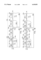
- FIGS. 1A to 1F are schematic, cross-sectional views of illustrating the process steps of fabricating the integration of high-voltage devices and low-voltage devices according to a preferred embodiment of this invention.
- At least one high-voltage device region 105a and at least one low-voltage device region 105b are formed in the substrate 100 having an electrical property of a type-I dopant.
- At least one type-II dopant well 110a is formed in the high-voltage device region 105a, and at least one type-II dopant well 110b is formed in the low-voltage device region 105b, by, for example, ion implantation.
- a pad oxide layer 120 and a masking layer 130 are formed sequentially on the substrate 100.
- the material of pad oxide layer 120 can be silicon oxide formed by, for example, thermal oxidation.
- a preferable material for masking layer 130 can be, for example, silicon nitride formed by, for instance, low pressure chemical vapor deposition.
- openings 145a, 145b, 155a, 155b, 165c are formed inside the masking layer 130, exposing the surface of pad oxide layer 120.
- a patterned photoresist layer 140 is formed over the substrate 100, with openings 145a, 145b exposed in the high-voltage device region 105a and opening 145c exposed in the low-voltage device region 105b.
- type-I dopant drafting doping regions 140a are formed in the type-II dopant well 110a inside the high-voltage device region 105a.
- type-I dopant isolation doping regions 140b are formed in the type-I dopant substrate 100 inside the high-voltage device region 105a along with a type-I dopant anti-punch-through doping region 140c formed in the type-I dopant substrate 100 inside the low-voltage device region 105b.
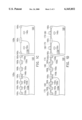
- photoresist layer 140 is removed first, and then a patterned photoresist layer 150 is formed over the substrate 100, with openings 155a, 155b exposed in the high-voltage device region 105a and opening 155c exposed in the low-voltage device region 105b.
- type-II dopant drafting doping regions 150a are formed in type-I dopant substrate 100 inside the high-voltage device region 105a.
- type-II dopant isolation doping regions 150b are formed in the type-II dopant well 110a inside the high-voltage device region 105a along with a type-II dopant anti-punch-through doping region 150c formed in the type-II dopant well 110b inside the low-voltage device region 105b.
- isolation structures 160a, 160b, 160c are formed subsequently in the exposed substrate 100, wherein isolation structures 160a, 160b, 160c can be, for example, field oxide layers or shallow trench isolation.
- masking layer 130 and pad oxide layer 120 are removed.
- the material of masking layer 130 is silicon nitride
- hot phosphoric acid can be used.
- the material of pad oxide layer 120 is silicon oxide, then hydrofluoric acid can be applied to remove pad oxide layer 120.
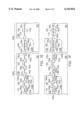
- a gate oxide layer 170 and a plurality of gates 180 are formed subsequently over the substrate 100.
- a method of forming gate oxide layer 170 can be, for instance, thermal oxidation.
- a preferable material of gate 180 can be, for example, doped polysilicon or polycide, formed by, for example, chemical vapor deposition.
- a patterned photoresist layer 185 is formed over the substrate 100. Later on, the third ion implantation step is performed to implant type-I dopant in the substrate 100. Hence type-I dopant source/drain doping region 190a, 190b are formed accordingly in the type-II dopant well 110a inside the high-voltage device region 105a and in the type-II dopant well 110b inside the low-voltage device region 105b.
- a patterned photoresist layer 195 is formed.
- the fourth ion implantation step is performed to implant type-II dopant in the substrate 100.
- a plurality of type-II dopant source/drain doping regions 200a, 200b are formed in the type-I dopant substrate 100 inside the high-voltage device region 105a and the low-voltage device region 105b.
- the type-I dopant is an n-type dopant
- the type-II dopant is a p-type dopant.
- the type-II dopant is an n-type dopant.
- the n-type dopant can be, for example, a phosphorus dopant or an arsenic dopant.
- the p-type dopant can be, for instance, a boron dopant.
- the dopant dose is about 3 ⁇ 10 13 to about 9 ⁇ 10 13 atom/cm 2 , with an implantation energy of about 20 to about 50 keV. If the p-type dopant is used for the first and the second ion implantation steps, the dopant dose is about 1 ⁇ 10 12 to about 5 ⁇ 10 12 atom/cm 2 , with an implantation energy of about 120 to about 180 keV.
- the dopant dose is about 1 ⁇ 10 15 to about 3 ⁇ 10 15 atom/cm 2 , with an implantation energy of about 60 to about 100 keV. If the p-type dopant is used for the third and the fourth ion implantation steps, the dopant dose is about 3 ⁇ 10 15 to about 5 ⁇ 10 15 atom/cm 2 , with an implantation energy of about 60 to about 100 keV.
- the dopant doses and the implantation energies described above are detailed in U.S. Pat. No. 5,382,820.
- this invention can be applied in the process of integrating the high-voltage device and the low-voltage device below 0.35 micron.
- the ion implantation steps for forming the isolation doping regions and the drafting doping regions in the high-voltage device are used to form simultaneously the anti-punch-through regions in the low-voltage device. Since the ion implantation steps for the high-voltage device and for the low-voltage device are integrated together, the ion implantation steps need not be performed separately to match different electrical property requirements for the high-voltage device and the low-voltage device.
- this invention has the advantage of simplifying the processes for integration of the high-voltage device and the low-voltage device. Therefore, this invention offers great help for increasing production.
Landscapes
- Metal-Oxide And Bipolar Metal-Oxide Semiconductor Integrated Circuits (AREA)
Abstract
The invention describes a method of fabricating the integration of high-voltage devices and low-voltage devices. The ion implantation steps for forming the isolation doping regions and the drafting doping regions in the high-voltage device are used to form simultaneously the anti-punch-through regions in the low-voltage device. The production of the integrated circuit is then finished with other process steps.
Description
This application claims the priority benefit of Taiwan application serial no. 89104138, filed Mar. 8, 2000.
1. Field of Invention
The present invention relates to a method of fabricating a metal-oxide-semiconductor (MOS) device. More particularly, the present invention relates to a method of fabricating the integration of the high-voltage devices and the low-voltage devices.
2. Description of Related Art
As the size of the MOS devices become smaller, the operation speed of the transistors becomes faster due to the reduced channel length. However, the short channel effects derived from the reduced channel length become severe. According to the equation (electric field=voltage/channel length), the electric field is proportional to the voltage and inversely proportional to the channel length. Therefore, if the voltage applied remains constant, the intensity of the electric field will increase due to the reduced channel length, which raises the energy of the electrons in the channel and further induces electrical breakdown as well as punch-through problems.
In general, for preventing short channel effects of the high-voltage MOS device, isolation structures are mainly used, which increase the distance between the gate and the source/drain and further decrease the transverse electric field in the channel. Consequently, the MOS device can still perform normally, even during high-voltage operation.
For the integrated circuits, if the high-voltage device and the low-voltage device are to be produced simultaneously, the production process applied for the low-voltage device is limited to the level of 0.5 to 0.6 micron. Integrated circuits containing both high-voltage and low-voltage devices are not rare. For example, the low-voltage device is used in the control circuits as the high-voltage device is used in electrically programmable read only memory (EPROM), flash memory or the driving circuits of the liquid crystal display.
In order to increase the integrity of the device, it is necessary to apply a production process of a smaller size, for instance, below 0.35 micron. However, anti-punch-through doping or multi-step well doping must be applied to produce a low-voltage device in such a small size to adjust the electrical properties of the device, and to prevent the punch-through problems that occur in the low-voltage device.
Usually, the high-voltage device and the low-voltage device are manufactured separately due to different electrical properties required for the high-voltage device and the low-voltage device and then are incorporated onto the same chip. For that reason, the manufacture steps become trivial and the control over the conditions of the process becomes complicated, increasing difficulties in the control over the manufacture conditions.
The invention provides a method of fabricating the integration of the high-voltage devices and the low-voltage devices, which combines the process steps, previously separate in the prior arts, for manufacturing the high-voltage device and the low-voltage device and hence simplifies the production process of the whole integrated circuit. For the processes of integrating the high-voltage device and the low-voltage device below 0.35 micron, this invention has the advantage that the anti-punch-through regions in the low-voltage device, and the isolation doping regions and the drafting doping regions in the high-voltage device are formed simultaneously. This invention offers great helps for increasing the production and the integrated circuit integrity.
As embodied and broadly described herein, the substrate contains at lease one high-voltage device region and one low-voltage device region, with at least one type-I dopant region and one type-II dopant region formed in each region. After a masking layer is formed on the substrate, a plurality of openings are formed inside the masking layer, exposing the surface of the substrate.
Later on, the first ion implantation step is performed to implant type-I dopant to the substrate. Hence type-I dopant drafting doping regions are formed in type-II dopant region inside the high-voltage device region. Simultaneously, type-I dopant isolation doping regions are formed in the type-I dopant region inside the high-voltage device region along with a type-I dopant anti-punch-through doping region formed in the type I dopant region inside the low-voltage device region.
The second ion implantation step is performed to implant type-II dopant in the substrate. Hence type-II dopant drafting doping regions are formed in the type-I dopant region inside the high-voltage device region. Simultaneously, type-II dopant isolation doping regions are formed in the type-II dopant region inside the high-voltage device region along with a type-II dopant anti-punch-through doping region formed in the type-II dopant region inside the low-voltage device region.
Several isolation structures are formed in the exposed substrate. After the masking layer is removed, a gate oxide layer and a plurality of gates are formed sequentially over the substrate. The third ion implantation step is performed to implant type-I dopant in the substrate, hence a plurality of type-I dopant source/drain doping regions are formed in the type-II dopant region. The fourth ion implantation step is performed to implant type-II dopant in the substrate. Hence a plurality of type-II dopant source/drain doping regions are formed in the type-I dopant region.
As embodied and broadly described herein, if the type-I dopant is an n-type dopant, then the type-II dopant is a p-type dopant. Conversely, if the type-I dopant is a p-type dopant, then the type-II dopant is an n-type dopant. The N-type dopant can be, for example, a phosphorus dopant or an arsenic dopant. P-type dopant can be, for instance, a boron dopant.
As embodied and broadly described herein, if an n-type dopant is used for the first and the second ion implantation steps, the dopant dose is about 3×10¹³ to about 9×10¹³ atom/cm2, with an implantation energy of about 20 to about 50 keV. If a p-type dopant is used for the first and the second ion implantation steps, the dopant dose is about 1×10¹² to about 5×10¹² atom/cm2, with an implantation energy of about 120 to about 180 keV. If an n-type dopant is used for the third and the fourth ion implantation steps, the dopant dose is about 1×10¹⁵ to about 3×10¹⁵ atom/cm2, with an implantation energy of about of 60 to about 100 keV. If a p-type dopant is used for the third and the fourth ion implantation steps, the dopant dose is about 3×10¹⁵ to about 5×10¹⁵ atom/cm2, with an implantation energy of about 60 to about 100 keV.
It is to be understood that both the foregoing general description and the following detailed description are exemplary, and are intended to provide further explanation of the invention as claimed.
The accompanying drawings are included to provide a further understanding of the invention, and are incorporated in and constitute a part of this specification. The drawings illustrate embodiments of the invention and, together with the description, serve to explain the principles of the invention. In the drawings,
FIGS. 1A to 1F are schematic, cross-sectional views of illustrating the process steps of fabricating the integration of high-voltage devices and low-voltage devices according to a preferred embodiment of this invention.
Referring to FIG. 1A, at least one high-voltage device region 105a and at least one low-voltage device region 105b are formed in the substrate 100 having an electrical property of a type-I dopant. At least one type-II dopant well 110a is formed in the high-voltage device region 105a, and at least one type-II dopant well 110b is formed in the low-voltage device region 105b, by, for example, ion implantation.
Again referring to FIG.. 1A, a pad oxide layer 120 and a masking layer 130 are formed sequentially on the substrate 100. The material of pad oxide layer 120 can be silicon oxide formed by, for example, thermal oxidation. A preferable material for masking layer 130 can be, for example, silicon nitride formed by, for instance, low pressure chemical vapor deposition.
Several openings 145a, 145b, 155a, 155b, 165c are formed inside the masking layer 130, exposing the surface of pad oxide layer 120. A patterned photoresist layer 140 is formed over the substrate 100, with openings 145a, 145b exposed in the high-voltage device region 105a and opening 145c exposed in the low-voltage device region 105b.
Later on, the first ion implantation step is performed to implant type-I dopant in the substrate 100. Hence type-I dopant drafting doping regions 140a are formed in the type-II dopant well 110a inside the high-voltage device region 105a. Simultaneously, type-I dopant isolation doping regions 140b are formed in the type-I dopant substrate 100 inside the high-voltage device region 105a along with a type-I dopant anti-punch-through doping region 140c formed in the type-I dopant substrate 100 inside the low-voltage device region 105b.
Referring to FIG. 1B, photoresist layer 140 is removed first, and then a patterned photoresist layer 150 is formed over the substrate 100, with openings 155a, 155b exposed in the high-voltage device region 105a and opening 155c exposed in the low-voltage device region 105b.
Later on, the second ion implantation step is performed to implant type-II dopant in the substrate 100. Hence type-II dopant drafting doping regions 150a are formed in type-I dopant substrate 100 inside the high-voltage device region 105a. Simultaneously, type-II dopant isolation doping regions 150b are formed in the type-II dopant well 110a inside the high-voltage device region 105a along with a type-II dopant anti-punch-through doping region 150c formed in the type-II dopant well 110b inside the low-voltage device region 105b.
Referring to FIG. 1C, after photoresist layer 150 is removed, a plurality of isolation structures 160a, 160b, 160c are formed subsequently in the exposed substrate 100, wherein isolation structures 160a, 160b, 160c can be, for example, field oxide layers or shallow trench isolation. Afterwards, masking layer 130 and pad oxide layer 120 are removed. For removing masking layer 130, if the material of masking layer 130 is silicon nitride, hot phosphoric acid can be used. If the material of pad oxide layer 120 is silicon oxide, then hydrofluoric acid can be applied to remove pad oxide layer 120.
Referring to FIG.. 1D, a gate oxide layer 170 and a plurality of gates 180 are formed subsequently over the substrate 100. A method of forming gate oxide layer 170 can be, for instance, thermal oxidation. A preferable material of gate 180 can be, for example, doped polysilicon or polycide, formed by, for example, chemical vapor deposition.
Referring to FIG.. 1E, a patterned photoresist layer 185 is formed over the substrate 100. Later on, the third ion implantation step is performed to implant type-I dopant in the substrate 100. Hence type-I dopant source/drain doping region 190a, 190b are formed accordingly in the type-II dopant well 110a inside the high-voltage device region 105a and in the type-II dopant well 110b inside the low-voltage device region 105b.
Referring to FIG.. 1F, after photoresist layer 185 is removed, a patterned photoresist layer 195 is formed. The fourth ion implantation step is performed to implant type-II dopant in the substrate 100. Hence, a plurality of type-II dopant source/drain doping regions 200a, 200b are formed in the type-I dopant substrate 100 inside the high-voltage device region 105a and the low-voltage device region 105b.
The following process steps for removing photoresist layer 195 and for finishing the production of this integrated circuit are well known to those persons who are familiar with the prior arts, therefore, they will not be illustrated here.
In the preferred embodiment described herein, if the type-I dopant is an n-type dopant, then the type-II dopant is a p-type dopant. Conversely, if the type-I dopant is a p-type dopant, then the type-II dopant is an n-type dopant. The n-type dopant can be, for example, a phosphorus dopant or an arsenic dopant. The p-type dopant can be, for instance, a boron dopant.
In the preferred embodiment described herein, if the n-type dopant is used for the first and the second ion implantation steps, the dopant dose is about 3×10¹³ to about 9×10¹³ atom/cm2, with an implantation energy of about 20 to about 50 keV. If the p-type dopant is used for the first and the second ion implantation steps, the dopant dose is about 1×10¹² to about 5×10¹² atom/cm2, with an implantation energy of about 120 to about 180 keV. If the n-type dopant is used for the third and the fourth ion implantation steps, the dopant dose is about 1×10¹⁵ to about 3×10¹⁵ atom/cm2, with an implantation energy of about 60 to about 100 keV. If the p-type dopant is used for the third and the fourth ion implantation steps, the dopant dose is about 3×10¹⁵ to about 5×10¹⁵ atom/cm2, with an implantation energy of about 60 to about 100 keV. The dopant doses and the implantation energies described above are detailed in U.S. Pat. No. 5,382,820.
In the preferred embodiment described herein, this invention can be applied in the process of integrating the high-voltage device and the low-voltage device below 0.35 micron. In this invention, the ion implantation steps for forming the isolation doping regions and the drafting doping regions in the high-voltage device are used to form simultaneously the anti-punch-through regions in the low-voltage device. Since the ion implantation steps for the high-voltage device and for the low-voltage device are integrated together, the ion implantation steps need not be performed separately to match different electrical property requirements for the high-voltage device and the low-voltage device.
In conclusion, this invention has the advantage of simplifying the processes for integration of the high-voltage device and the low-voltage device. Therefore, this invention offers great help for increasing production.
It will be apparent to those skilled in the art that various modifications and variations can be made to the structure of the present invention without departing from the scope or spirit of the invention. In view of the foregoing, it is intended that the present invention cover modifications and variations of this invention provided they fall within the scope of the following claims and their equivalents.
Claims (17)
1. A method of fabricating the integration of high-voltage devices and low-voltage devices, wherein a provided substrate contains at least one high-voltage device region and at least one low-voltage device region, with at least one type-I dopant region and at least one type-II dopant region formed in each region, the method comprising:
forming a masking layer on the substrate;
forming a plurality of openings inside the masking layer to expose the surface of the substrate;
performing a first ion implantation step to implant the type-I dopant in the substrate, two type-I dopant drafting doping regions being formed in a type-II dopant region inside the high-voltage device region, two type-I dopant isolation doping regions being formed in a type-I dopant region inside the high-voltage device region, and a type-I dopant anti-punch-through doping region being formed in a type-I dopant region inside the low-voltage device region;
performing a second ion implantation step to implant the type-II dopant in the substrate, two type-II dopant drafting doping regions being formed in type-I dopant region inside the high-voltage device region, two type-II dopant isolation doping regions being formed in the type-II dopant region inside the high-voltage device region, and a type-II dopant anti-punch-through doping region being formed in the type-II dopant region inside the low-voltage device region;
forming a plurality of isolation structures in the substrate exposed;
removing the masking layer;
forming a gate oxide layer over the substrate;
forming a plurality of gates over the substrate;
performing a third ion implantation step to implant the type-I dopant in the substrate, which forms a plurality of type-I dopant source/drain regions in the type-II dopant regions; and
performing a fourth ion implantation step to implant the type-II dopant in the substrate, which forms a plurality of type-II dopant source/drain regions in the type-I dopant regions.
2. The method as claimed in 1, wherein if the type-I dopant is an n-type dopant, then the type-II dopant is a p-type dopant.
3. The method as claimed in 1, wherein if the type-I dopant is a p-type dopant, then the type-II dopant is an n-type dopant.
4. The method as claimed in 2, wherein the n-type dopant is a phosphorus dopant or an arsenic dopant.
5. The method as claimed in 3, wherein the n-type dopant is a phosphorus dopant or an arsenic dopant.
6. The method as claimed in 2, wherein the p-type dopant is a boron dopant.
7. The method as claimed in 3, wherein the p-type dopant is a boron dopant.
8. The method as claimed in 2, wherein a dopant dose of the type-I dopant applied in the first ion implantation step is about 3×10¹³ to about 9×10¹³ atom/cm2, with an implantation energy of about 20 to about 50 keV.
9. The method as claimed in 2, wherein a dopant dose of type-II dopant for the second ion implantation step is about 1×10¹² to about 5×10¹² atom/cm2, with an implantation energy of about 120 to about 180 keV.
10. The method as claimed in 2, wherein the dopant dose of the type-I dopant for the third ion implantation step is about 1×10¹⁵ to about 3×10¹⁵ atom/cm2, with an implantation energy of about 60 to about 100 keV.
11. The method as claimed in 2, wherein a dopant dose of the type-II dopant for the fourth ion implantation step is about 3×10¹⁵ to about 5×10¹⁵ atom/cm2, with an implantation energy of about 60 to about 100 keV.
12. The method as claimed in 3, wherein the dopant dose of type-I dopant for the first ion implantation step is about 1×10¹² to about 5×10¹² atom/cm2, with an implantation energy of about 120 to about 180 keV.
13. The method as claimed in 3, wherein a dopant dose of the type-II dopant for the second ion implantation step is about 3×10¹³ to about 9×10¹³ atom/cm2, with an implantation energy of about 20 to about 50 keV.
14. The method as claimed in 3, wherein a dopant dose of the type-I dopant for the third ion implantation step is about 1×10¹⁵ to about 3×10¹⁵ atom/cm2, with an implantation energy of about 60 to about 100 keV.
15. The method as claimed in 3, wherein a dopant dose of the type-II dopant for the fourth ion implantation step is about 3×10¹⁵ to about 5×10¹⁵ atom/cm2, with an implantation energy of about 60 to about 100 keV.
16. A method of simultaneously improving the electrical properties for high-voltage devices and low-voltage devices, wherein a high-voltage device region and a low-voltage device region, each containing a n-type dopant region and a p-type dopant region, are formed on the provided substrate, the method comprising:
performing a first ion implantation step to implant the n-type dopant in the substrate, two n-type dopant drafting doping regions being formed in the p-type dopant region inside the high-voltage device region, two n-type dopant isolation doping regions being formed in the n-type dopant region inside the high-voltage device region, and an n-type dopant anti-punch-through doping region being formed in the n-type dopant region inside the low-voltage device region, wherein the dopant dose is about 3×10¹³ to about 9×10¹³ atom/cm2, with an implantation energy of about 20 to about 50 keV; and
performing a second ion implantation step to implant the p-type dopant in the substrate, two p-type dopant drafting doping regions being formed in the n-type dopant region inside the high-voltage device region, two p-type dopant isolation doping regions being formed in the p-type dopant region inside the high-voltage device region, and a p-type dopant anti-punch-through doping region being formed in the p-type dopant region inside the low-voltage device region, wherein a dopant dose of a p-type dopant for the second ion implantation step is about 1×10¹² to about 5×10¹² atom/cm2, with an implantation energy of about 120 to about 180 keV.
17. A method of simultaneously improving the electrical properties for high-voltage devices and low-voltage devices, wherein a high-voltage device region and a low-voltage device region, each containing a p-type dopant region and a n-type dopant region, are formed on the provided substrate, the method comprising:
performing a first ion implantation step to implant the p-type dopant in the substrate, two p-type dopant drafting doping regions being formed in the n-type dopant region inside the high-voltage device region, two p-type dopant isolation doping regions being formed in the p-type dopant region inside the high-voltage device region, a p-type dopant anti-punch-through doping region being formed in the p-type dopant region inside the low-voltage device region, wherein a dopant dose of p-type dopant for the second ion implantation step is about 1×10¹² to about 5×10¹² atom/cm2, with an implantation energy of about 120 to about 180 keV; and
performing one second ion implantation step to implant the n-type dopant in the substrate, two n-type dopant drafting doping regions being formed in the p-type dopant region inside the high-voltage device region, two n-type dopant isolation doping regions being formed in the n-type dopant region inside the high-voltage device region, and an n-type dopant anti-punch-through doping region being formed in the n-type dopant region inside the low-voltage device region, wherein a dopant dose is about 3×10¹³ to about 9×10¹³ atom/cm2, with an implantation energy of about 20 to about 50 keV.
Applications Claiming Priority (2)
| Application Number | Priority Date | Filing Date | Title |
|---|---|---|---|
| TW089104138A TW451268B (en) | 2000-03-08 | 2000-03-08 | Integrated manufacturing method of high-voltage device and low-voltage device |
| TW89104138 | 2000-03-08 |
Publications (1)
| Publication Number | Publication Date |
|---|---|
| US6165852A true US6165852A (en) | 2000-12-26 |
Family
ID=21659014
Family Applications (1)
| Application Number | Title | Priority Date | Filing Date |
|---|---|---|---|
| US09/557,343 Expired - Lifetime US6165852A (en) | 2000-03-08 | 2000-04-25 | Method of fabricating integration of high-voltage devices and low-voltage devices |
Country Status (2)
| Country | Link |
|---|---|
| US (1) | US6165852A (en) |
| TW (1) | TW451268B (en) |
Cited By (3)
| Publication number | Priority date | Publication date | Assignee | Title |
|---|---|---|---|---|
| US6440802B1 (en) * | 2000-08-28 | 2002-08-27 | Sharp Kabushiki Kaisha | Process for fabricating semiconductor device and photolithography mask |
| US6803282B2 (en) * | 2001-12-07 | 2004-10-12 | Texas Instruments Incorporated | Methods for fabricating low CHC degradation mosfet transistors |
| US20060222495A1 (en) * | 2005-03-29 | 2006-10-05 | Siemens Westinghouse Power Corporation | Turbine blade cooling system with bifurcated mid-chord cooling chamber |
-
2000
- 2000-03-08 TW TW089104138A patent/TW451268B/en not_active IP Right Cessation
- 2000-04-25 US US09/557,343 patent/US6165852A/en not_active Expired - Lifetime
Cited By (3)
| Publication number | Priority date | Publication date | Assignee | Title |
|---|---|---|---|---|
| US6440802B1 (en) * | 2000-08-28 | 2002-08-27 | Sharp Kabushiki Kaisha | Process for fabricating semiconductor device and photolithography mask |
| US6803282B2 (en) * | 2001-12-07 | 2004-10-12 | Texas Instruments Incorporated | Methods for fabricating low CHC degradation mosfet transistors |
| US20060222495A1 (en) * | 2005-03-29 | 2006-10-05 | Siemens Westinghouse Power Corporation | Turbine blade cooling system with bifurcated mid-chord cooling chamber |
Also Published As
| Publication number | Publication date |
|---|---|
| TW451268B (en) | 2001-08-21 |
Similar Documents
| Publication | Publication Date | Title |
|---|---|---|
| USH986H (en) | Field effect-transistor with asymmetrical structure | |
| US6518623B1 (en) | Semiconductor device having a buried-channel MOS structure | |
| EP0978141B1 (en) | Method of making nmos and pmos devices with reduced masking steps | |
| US7091079B2 (en) | Method of forming devices having three different operation voltages | |
| US5296401A (en) | MIS device having p channel MOS device and n channel MOS device with LDD structure and manufacturing method thereof | |
| US5047358A (en) | Process for forming high and low voltage CMOS transistors on a single integrated circuit chip | |
| US7851317B2 (en) | Method for fabricating high voltage drift in semiconductor device | |
| US6204133B1 (en) | Self-aligned extension junction for reduced gate channel | |
| US5885887A (en) | Method of making an igfet with selectively doped multilevel polysilicon gate | |
| US7256092B2 (en) | Method for fabricating integrated circuits having both high voltage and low voltage devices | |
| US6051459A (en) | Method of making N-channel and P-channel IGFETs using selective doping and activation for the N-channel gate | |
| US5185279A (en) | Method of manufacturing insulated-gate type field effect transistor | |
| US5956591A (en) | Method of making NMOS and PMOS devices having LDD structures using separate drive-in steps | |
| US6509243B2 (en) | Method for integrating high-voltage device and low-voltage device | |
| US6008100A (en) | Metal-oxide semiconductor field effect transistor device fabrication process | |
| US5977600A (en) | Formation of shortage protection region | |
| US5970331A (en) | Method of making a plug transistor | |
| JP2836515B2 (en) | Method for manufacturing semiconductor device | |
| US5393679A (en) | Use of double charge implant to improve retrograde process PMOS punch through voltage | |
| US6165852A (en) | Method of fabricating integration of high-voltage devices and low-voltage devices | |
| US6124159A (en) | Method for integrating high-voltage device and low-voltage device | |
| US20030116800A1 (en) | Semiconductor device and method for fabricating the same | |
| KR100415191B1 (en) | Method for fabricating asymmetric cmos transistor | |
| US20060148185A1 (en) | Method for manufacturing high voltage transistor | |
| KR100959241B1 (en) | Manufacturing Method of Semiconductor Device |
Legal Events
| Date | Code | Title | Description |
|---|---|---|---|
| AS | Assignment |
Owner name: UNITED MICROELECTRONICS CORP., TAIWAN Free format text: ASSIGNMENT OF ASSIGNORS INTEREST;ASSIGNORS:CHEN, SHENG-LUNG;YANG, SHENG-HSING;REEL/FRAME:010767/0133 Effective date: 20000414 |
|
| STCF | Information on status: patent grant |
Free format text: PATENTED CASE |
|
| FEPP | Fee payment procedure |
Free format text: PAYOR NUMBER ASSIGNED (ORIGINAL EVENT CODE: ASPN); ENTITY STATUS OF PATENT OWNER: LARGE ENTITY |
|
| FPAY | Fee payment |
Year of fee payment: 4 |
|
| FPAY | Fee payment |
Year of fee payment: 8 |
|
| FPAY | Fee payment |
Year of fee payment: 12 |