US6153492A - Method for improving the readability of alignment marks - Google Patents
Method for improving the readability of alignment marks Download PDFInfo
- Publication number
- US6153492A US6153492A US09/492,656 US49265600A US6153492A US 6153492 A US6153492 A US 6153492A US 49265600 A US49265600 A US 49265600A US 6153492 A US6153492 A US 6153492A
- Authority
- US
- United States
- Prior art keywords
- etching
- alignment marks
- metal
- alignment
- semiconductor wafer
- Prior art date
- Legal status (The legal status is an assumption and is not a legal conclusion. Google has not performed a legal analysis and makes no representation as to the accuracy of the status listed.)
- Expired - Lifetime
Links
Images
Classifications
-
- H—ELECTRICITY
- H10—SEMICONDUCTOR DEVICES; ELECTRIC SOLID-STATE DEVICES NOT OTHERWISE PROVIDED FOR
- H10W—GENERIC PACKAGES, INTERCONNECTIONS, CONNECTORS OR OTHER CONSTRUCTIONAL DETAILS OF DEVICES COVERED BY CLASS H10
- H10W46/00—Marks applied to devices, e.g. for alignment or identification
-
- H—ELECTRICITY
- H10—SEMICONDUCTOR DEVICES; ELECTRIC SOLID-STATE DEVICES NOT OTHERWISE PROVIDED FOR
- H10W—GENERIC PACKAGES, INTERCONNECTIONS, CONNECTORS OR OTHER CONSTRUCTIONAL DETAILS OF DEVICES COVERED BY CLASS H10
- H10W46/00—Marks applied to devices, e.g. for alignment or identification
- H10W46/301—Marks applied to devices, e.g. for alignment or identification for alignment
-
- H—ELECTRICITY
- H10—SEMICONDUCTOR DEVICES; ELECTRIC SOLID-STATE DEVICES NOT OTHERWISE PROVIDED FOR
- H10W—GENERIC PACKAGES, INTERCONNECTIONS, CONNECTORS OR OTHER CONSTRUCTIONAL DETAILS OF DEVICES COVERED BY CLASS H10
- H10W46/00—Marks applied to devices, e.g. for alignment or identification
- H10W46/501—Marks applied to devices, e.g. for alignment or identification for use before dicing
Definitions
- the invention lies in the field of semiconductor manufacture. More specifically, the invention relates to a method for improving the identifiability or readability of alignment marks on semiconductor wafers during multilayer metallization, in which the alignment marks are fabricated in the scribe line and vias or contact holes or plated-through holes to deeper metallization layers or active regions by means of a photolithographic patterning step in an oxide layer by etching and subsequent deposition of metal, and in which the semiconductor wafer is subsequently planarized in a CMP step (polishing step), with subsequent aluminum (Al) metallization.
- CMP step polishing step
- Alignment marks are indispensable for the photolithographic processing of semiconductor wafers. Alignment marks help ensure that the masks which are necessary for exposing the photoresist on the semiconductor wafer can be aligned exactly with respect to the latter. This presupposes that the alignment marks have an exact assignment to the structures to be fabricated on the semiconductor wafer and, furthermore, offer a sufficient topographical contrast to be able to be reliably identified. After each CMP process, in particular, the identification of these alignment marks is greatly impaired due to the topographical contrast which is severely reduced or absent on account of the polishing operation. The consequence is an increased outlay on postprocessing on account of the misalignment of the mask. It may even happen that alignment becomes completely impossible. This problem is becoming ever greater, however, on account of the ever decreasing structure widths and the consequentially increasing requirements made of the alignment accuracy.
- the alignment marks are located at such a depth that a topography which offers a sufficient contrast still remains after the CMP process. See FIG. 1. It is disadvantageous in that case, however, that the inner edges of the alignment marks can be displaced or flattened in an uncontrolled manner due to unavoidable asymmetric erosion of the oxide surrounding the alignment mark. An overlay error is consequently produced during wafer exposure. Such an error necessitates post processing of the semiconductor wafer. In this case, this overlay error on account of displacement of the detected edge position can occur either at the alignment marks within a wafer, or from wafer to wafer or from batch to batch.
- a further disadvantage of particularly deep alignment marks may be seen in the fact that considerable quantities of particles and slurry residues may remain in the alignment marks, particularly after the CMP process, and involve the risk of contamination and an increased defect density. Since these particles can also settle on the edges of the alignment mark, this results in further flattening of the edges. The consequence is that exact alignment is at the very least made more difficult, if not even impossible. Consequently, the readability of the alignment marks cannot be improved sufficiently by that method.
- an additional photoplane is used. See FIG. 2.
- a further alignment mark (auxiliary mark) is etched in the scribe line before metallization and is intended to allow better alignment after metallization due to sharper edges.
- auxiliary mark is etched in the scribe line before metallization and is intended to allow better alignment after metallization due to sharper edges.
- the additional alignment mark can be aligned more easily relative to the tungsten-filled marker, owing to the fact that the material contrast between the additional alignment mark and the surrounding oxide can be utilized.
- the outlay for the additional photoplane and the fact that the overlay error of the two markers accumulates are disadvantageous in this case.
- the object of the invention is to provide a method for improving the readability of alignment marks on semiconductor wafers for the purpose of better alignment after metallization in semiconductor manufacture, which overcomes the above-noted deficiencies and disadvantages of the prior art devices and methods of this kind, and which does not influence the functionality of the semiconductor chips to be fabricated and is also simple and cost-effective to realize. It is a further object to provide a method which simultaneously enables the defects and contamination based on particles and slurry residues to be largely eliminated.
- a method for improving the readability of alignment marks on semiconductor wafers during multilayer metallization which comprises:
- metal situated in the alignment marks is etched back for the purpose of uncovering the edges of the alignment marks after the deposition of metal and the subsequent CMP step.
- a sharply defined edge is produced in the transition from the oxide to the metal within the alignment mark, which edge can be used to effect exact and reproducible alignment of the photoplanes relative to the contact hole or via plane after metallization.
- the etching-back step which is not necessary for the function of the semiconductor chip to be fabricated, produces a sharply defined edge in a simple manner. This results in a considerable reduction in the reworking rates in the critical metallization planes.
- there is no residual topology present after the CMP process with the result that no particles can accumulate in the alignment marks either.
- tungsten is deposited during the deposition of metal in the alignment marks and the vias or contact holes, where the subsequent etching back process is effected selectively in such a way that preferentially relatively large areas are etched.
- the effect achieved as a result of this is that preferably the tungsten in the alignment marks is etched, since there is no desire for any etching back in the contact holes or vias.
- the method is also wherein the etching back process is performed with high selectivity with respect to the material surrounding the alignment mark, in particular the surrounding oxide.
- the etching is performed in a reactive ion etching (RIE) system or in an inductive coupled plasma source (ICP) system in a Cl 2 /SF 6 /NF 3 atmosphere, which ensures sufficient etching selectivity with respect to the surrounding oxide.
- RIE reactive ion etching
- ICP inductive coupled plasma source
- This etching selectivity may additionally be further improved by additive gases being added to the Cl 2 /SF 6 /NF 3 atmosphere.
- O 2 and/or N 2 are/is preferable as additive gases.
- complete planarization of the surface of the semiconductor wafer is performed in the CMP step before the etching back process. This reliably prevents particles from being taken up.
- the recess etching process is performed selectively with respect to the metal in the alignment mark and with respect to the liner, where it is preferable for a wet-chemical recess etching process using dilute hydrofluoric acid to be effected.
- the recess etching may also be performed by RIE etching or by etching from the vapor phase.
- the semiconductor wafer is covered by a photoresist, the relatively close surroundings of the alignment marks being kept free. In this case, it is not necessary to impose any special accuracy requirements on the region to be kept free.
- the region to be kept free for the recess etching may also be defined and patterned with the aid of standard lithography, where the exposure can be effected through a 1:1 mask on account of the inconsiderable accuracy requirements.
- the alignment marks are identified by a microscope optical arrangement and the surroundings thereof are exposed by the microscope optical arrangement.
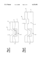
- FIG. 1 is a diagrammatic view of a prior art alignment mark located particularly deep, with alignment with the inner edges of the marker;
- FIG. 2 is a diagrammatic view illustrating a prior art method by means of an auxiliary marker in an additional photoplane
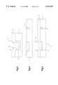
- FIG. 3 is a diagrammatic view of an etched-back alignment mark with good topological contrast and with a metallization layer
- FIG. 4 is a diagrammatic view of a shallow, tungsten-filled alignment mark after the CMP process
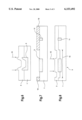
- FIG. 5 is a diagrammatic view of the etched-back alignment mark with good topological contrast according to FIG. 4 with a metallization layer;
- FIG. 6 is a diagrammatic view of an alignment mark with good topological contrast with recess-etched surroundings and a metallization layer;
- FIG. 7 is a diagrammatic view of a shallow alignment mark after the CMP process without topological contrast, with additional photoresist.
- FIG. 8 is a diagrammatic view of the alignment mark with good topological contrast according to FIG. 7 with recess-etched surroundings (oxide recess) and a metallization layer.
- alignment marks 5 prepared in each case by a method from the prior art, which already reflects the endeavor to achieve better identification of the alignment mark 5. Accordingly, in the case of the alignment mark 5 according to FIG. 1, first of all a particularly deep depression was produced in the oxide 1 by photolithography and subsequent etching and then tungsten 3 was deposited on the entire wafer. The tungsten on the wafer was subsequently removed by a CMP process, with the result that only the tungsten in the depression of the alignment mark 5 remains. In this case, however, particles may also be deposited in the alignment mark 5. The corresponding region is designated by the reference symbol 4 in FIG. 1. These deposits lead to flattening of the edges, with the consequence of poor identifiability (readability), since the shape of the depression of the alignment mark 5 and thus also the edges 6 of the alignment mark are reproduced in the metallization layer 2 applied over them.
- FIG. 2 shows the same alignment mark 5 once again, but with the latter having been assigned an auxiliary marker 7 in an additional photoplane.
- This auxiliary marker 7 has sharper edges, with the result that these can also be better identified in the Al metallization layer 2 situated over them.
- the additional alignment mark 5 can admittedly be aligned more easily relative to the tungsten-filled marker, since the material contrast between the auxiliary marker 7 and the surrounding oxide 1 can be utilized. The fact that the overlay error of the two markers accumulates is disadvantageous in this case.
- FIGS. 3 to 8 there are shown alignment marks 5 in which significantly better identification is ensured by the application of the methods according to the invention, and in which, in particular, the problems of particles being deposited in an uncontrolled manner after the CMP process can no longer occur.
- FIG. 3 shows a deep alignment mark 5 in the case of which the tungsten 3 situated in the depression in the alignment mark 5 has been etched back before Al metallization. Sharper outer edges 9 are produced in the process at the transitions to the surrounding oxide 1.
- This etching can be performed in a standard RIE/ICP system with a Cl 2 /SF 6 /NF 3 atmosphere, as a result of which it is possible to ensure sufficient etching selectivity with respect to the surrounding oxide 1.
- the etching selectivity can be further improved by the addition of additive gases, such as O 2 or N 2 .
- the subsequent etching back is effected until the edges 6 that are produced at the marker-oxide transition can be identified sufficiently well as topological contrast after Al metallization.
- FIGS. 6-8 show a variant of the exemplary method according to the invention in which the oxide 1 surrounding the alignment mark 5 has been etched back by recess etching, with the result that the alignment mark 5 projects approximately 100-500 nm from the surface.
- the recess etching may preferably be effected wet-chemically using dilute hydrofluoric acid selectively with respect to the tungsten and with respect to the liner.
- the recess etching process can be applied both to shallow and to deep alignment marks 5.
- FIG. 6 shows the application of the recess etching process to an existing deep alignment mark 5.
- the application of this method presupposes that the recess etching is restricted to the region of the alignment marks 5, since the contact holes or vias 11 are not permitted to project to such an extent from the surface.
- the alignment of the recess region 14 relative to the alignment marks 5 is completely noncritical as long as the markers to be identified are detected and are not etched too far into the chip region.
- the recess region 14 can be seen in
- FIGS. 7, 8 This region is defined and patterned e.g. using standard lithography.
- the recess etching can also be carried out by means of an RIE step or by etching from the vapor phase.
- the use of the shallow alignment mark 5 (see FIGS. 7, 8) furthermore has the advantage that no topology remains after the CMP process and, consequently, it is not possible for any contamination and particles to accumulate. In addition, only the edges to be detected are produced as contrast-affording topology.
Landscapes
- Exposure And Positioning Against Photoresist Photosensitive Materials (AREA)
- Exposure Of Semiconductors, Excluding Electron Or Ion Beam Exposure (AREA)
Abstract
Description
Claims (22)
Applications Claiming Priority (2)
| Application Number | Priority Date | Filing Date | Title |
|---|---|---|---|
| DE19903196A DE19903196A1 (en) | 1999-01-27 | 1999-01-27 | Alignment mark recognition, in photolithographic production of multilayer metallizations on wafers, is improved by back etching metal present in the marks to expose mark edges after metal deposition and CMP steps |
| DE19903196 | 1999-01-27 |
Publications (1)
| Publication Number | Publication Date |
|---|---|
| US6153492A true US6153492A (en) | 2000-11-28 |
Family
ID=7895547
Family Applications (1)
| Application Number | Title | Priority Date | Filing Date |
|---|---|---|---|
| US09/492,656 Expired - Lifetime US6153492A (en) | 1999-01-27 | 2000-01-27 | Method for improving the readability of alignment marks |
Country Status (2)
| Country | Link |
|---|---|
| US (1) | US6153492A (en) |
| DE (1) | DE19903196A1 (en) |
Cited By (18)
| Publication number | Priority date | Publication date | Assignee | Title |
|---|---|---|---|---|
| US6303459B1 (en) * | 1999-11-15 | 2001-10-16 | Taiwan Semiconductor Manufacturing Company | Integration process for Al pad |
| US6514780B2 (en) * | 1999-12-07 | 2003-02-04 | Infineon Technologies Ag | Method for manufacturing an integrated circuit having a particular functionality required by a user of the circuit and having first structures to produce the particular functionality and second structures |
| US20030066816A1 (en) * | 2001-09-17 | 2003-04-10 | Schultz Gary A. | Uniform patterning for deep reactive ion etching |
| US20030216009A1 (en) * | 2002-05-15 | 2003-11-20 | Hitachi, Ltd. | Semiconductor device and manufacturing the same |
| US20040022959A1 (en) * | 2002-05-15 | 2004-02-05 | Knut Kahlisch | Method of marking substandard parts |
| DE10259322A1 (en) * | 2002-12-18 | 2004-07-15 | Infineon Technologies Ag | Making alignment mark in opaque layer on substrate, forms trenches of differing depth, fills selectively, then adds and polishes further layers to leave defined opaque mark |
| US20040147072A1 (en) * | 2002-12-13 | 2004-07-29 | Christoph Kleint | Method for fabricating semiconductor memories with charge trapping memory cells |
| US20040188411A1 (en) * | 2002-10-02 | 2004-09-30 | Stratagene | Apparatus and method for flexible heating cover assembly for thermal cycling of samples of biological material |
| US20050074945A1 (en) * | 2003-10-06 | 2005-04-07 | Ching-Yu Chang | [overlay mark and method of fabricating the same] |
| US20070102819A1 (en) * | 2004-03-25 | 2007-05-10 | Klaus Goller | Method for producing an integrated circuit assembly with an auxiliary indentation, particularly with aligning marks, and an integrated circuit arrangement |
| US20070238286A1 (en) * | 2006-04-06 | 2007-10-11 | Hynix Semiconductor Inc. | Method of manufacturing semiconductor device |
| US20070247608A1 (en) * | 2006-04-03 | 2007-10-25 | Molecular Imprints, Inc. | Tesselated Patterns in Imprint Lithography |
| US20090032978A1 (en) * | 2007-07-31 | 2009-02-05 | International Business Machines Corporation | Microelectronic structure including dual damascene structure and high contrast alignment mark |
| WO2010073226A2 (en) | 2008-12-24 | 2010-07-01 | X-Fab Semiconductor Foundries Ag | Production of high alignment marks and such alignment marks on a semiconductor wafer |
| CN102376531A (en) * | 2010-08-12 | 2012-03-14 | 上海华虹Nec电子有限公司 | Method for improving photoetching marking signal after epitaxial filling and CMP (corrugated metal pipe) grinding |
| WO2015130510A1 (en) * | 2014-02-25 | 2015-09-03 | Weatherford/Lamb, Inc. | Alignment marking for rock sample analysis |
| CN107994031A (en) * | 2017-11-16 | 2018-05-04 | 长江存储科技有限责任公司 | A kind of 3D NAND manufacture methods |
| US11244907B2 (en) | 2020-01-02 | 2022-02-08 | International Business Machines Corporation | Metal surface preparation for increased alignment contrast |
Citations (4)
| Publication number | Priority date | Publication date | Assignee | Title |
|---|---|---|---|---|
| US5640053A (en) * | 1994-07-01 | 1997-06-17 | Cypress Semiconductor Corp. | Inverse open frame alignment mark and method of fabrication |
| US5663099A (en) * | 1990-06-29 | 1997-09-02 | Canon Kabushiki Kaisha | Method for producing semiconductor device having alignment mark |
| US5786260A (en) * | 1996-12-16 | 1998-07-28 | Taiwan Semiconductor Manufacturing Company, Ltd. | Method of fabricating a readable alignment mark structure using enhanced chemical mechanical polishing |
| US5911108A (en) * | 1997-01-29 | 1999-06-08 | Integrated Device Technology, Inc. | Method for protecting an alignment mark on a semiconductor substrate during chemical mechanical polishing and the resulting structure |
-
1999
- 1999-01-27 DE DE19903196A patent/DE19903196A1/en not_active Ceased
-
2000
- 2000-01-27 US US09/492,656 patent/US6153492A/en not_active Expired - Lifetime
Patent Citations (4)
| Publication number | Priority date | Publication date | Assignee | Title |
|---|---|---|---|---|
| US5663099A (en) * | 1990-06-29 | 1997-09-02 | Canon Kabushiki Kaisha | Method for producing semiconductor device having alignment mark |
| US5640053A (en) * | 1994-07-01 | 1997-06-17 | Cypress Semiconductor Corp. | Inverse open frame alignment mark and method of fabrication |
| US5786260A (en) * | 1996-12-16 | 1998-07-28 | Taiwan Semiconductor Manufacturing Company, Ltd. | Method of fabricating a readable alignment mark structure using enhanced chemical mechanical polishing |
| US5911108A (en) * | 1997-01-29 | 1999-06-08 | Integrated Device Technology, Inc. | Method for protecting an alignment mark on a semiconductor substrate during chemical mechanical polishing and the resulting structure |
Cited By (33)
| Publication number | Priority date | Publication date | Assignee | Title |
|---|---|---|---|---|
| US6303459B1 (en) * | 1999-11-15 | 2001-10-16 | Taiwan Semiconductor Manufacturing Company | Integration process for Al pad |
| US6514780B2 (en) * | 1999-12-07 | 2003-02-04 | Infineon Technologies Ag | Method for manufacturing an integrated circuit having a particular functionality required by a user of the circuit and having first structures to produce the particular functionality and second structures |
| US20030066816A1 (en) * | 2001-09-17 | 2003-04-10 | Schultz Gary A. | Uniform patterning for deep reactive ion etching |
| US6821867B2 (en) * | 2002-05-15 | 2004-11-23 | Renesas Technology Corp. | Method for forming grooves in the scribe region to prevent a warp of a semiconductor substrate |
| US20040022959A1 (en) * | 2002-05-15 | 2004-02-05 | Knut Kahlisch | Method of marking substandard parts |
| US20030216009A1 (en) * | 2002-05-15 | 2003-11-20 | Hitachi, Ltd. | Semiconductor device and manufacturing the same |
| US20040188411A1 (en) * | 2002-10-02 | 2004-09-30 | Stratagene | Apparatus and method for flexible heating cover assembly for thermal cycling of samples of biological material |
| US20040147072A1 (en) * | 2002-12-13 | 2004-07-29 | Christoph Kleint | Method for fabricating semiconductor memories with charge trapping memory cells |
| US7005355B2 (en) | 2002-12-13 | 2006-02-28 | Infineon Technologies Ag | Method for fabricating semiconductor memories with charge trapping memory cells |
| DE10259322B4 (en) * | 2002-12-18 | 2005-12-29 | Infineon Technologies Ag | A method of forming an alignment mark in an opaque layer on a substrate |
| DE10259322A1 (en) * | 2002-12-18 | 2004-07-15 | Infineon Technologies Ag | Making alignment mark in opaque layer on substrate, forms trenches of differing depth, fills selectively, then adds and polishes further layers to leave defined opaque mark |
| US20050074945A1 (en) * | 2003-10-06 | 2005-04-07 | Ching-Yu Chang | [overlay mark and method of fabricating the same] |
| US7459798B2 (en) * | 2003-10-06 | 2008-12-02 | Macronix International Co., Ltd. | Overlay mark |
| US7094662B2 (en) * | 2003-10-06 | 2006-08-22 | Ching-Yu Chang | Overlay mark and method of fabricating the same |
| US20070069399A1 (en) * | 2003-10-06 | 2007-03-29 | Ching-Yu Chang | Overlay mark |
| US20070102819A1 (en) * | 2004-03-25 | 2007-05-10 | Klaus Goller | Method for producing an integrated circuit assembly with an auxiliary indentation, particularly with aligning marks, and an integrated circuit arrangement |
| US7795105B2 (en) | 2004-03-25 | 2010-09-14 | Infineon Technologies Ag | Method for producing an integrated circuit assembly with an auxiliary indentation, particularly with aligning marks, and an integrated circuit arrangement |
| US20070247608A1 (en) * | 2006-04-03 | 2007-10-25 | Molecular Imprints, Inc. | Tesselated Patterns in Imprint Lithography |
| US8850980B2 (en) | 2006-04-03 | 2014-10-07 | Canon Nanotechnologies, Inc. | Tessellated patterns in imprint lithography |
| WO2007117523A3 (en) * | 2006-04-03 | 2008-04-10 | Molecular Imprints Inc | Imprint lithography system |
| US20070238286A1 (en) * | 2006-04-06 | 2007-10-11 | Hynix Semiconductor Inc. | Method of manufacturing semiconductor device |
| US7572729B2 (en) * | 2006-04-06 | 2009-08-11 | Hynix Semiconductor Inc. | Method of manufacturing semiconductor device |
| US7994639B2 (en) * | 2007-07-31 | 2011-08-09 | International Business Machines Corporation | Microelectronic structure including dual damascene structure and high contrast alignment mark |
| US20090032978A1 (en) * | 2007-07-31 | 2009-02-05 | International Business Machines Corporation | Microelectronic structure including dual damascene structure and high contrast alignment mark |
| DE102009060277A1 (en) | 2008-12-24 | 2010-09-02 | X-Fab Semiconductor Foundries Ag | Method for producing alignment marks for light-impermeable or light-absorbing layers (light shield resist masks) |
| WO2010073226A2 (en) | 2008-12-24 | 2010-07-01 | X-Fab Semiconductor Foundries Ag | Production of high alignment marks and such alignment marks on a semiconductor wafer |
| US8722506B2 (en) | 2008-12-24 | 2014-05-13 | X-Fab Semiconductor Foundries Ag | Production of high alignment marks and such alignment marks on a semiconductor wafer |
| CN102376531A (en) * | 2010-08-12 | 2012-03-14 | 上海华虹Nec电子有限公司 | Method for improving photoetching marking signal after epitaxial filling and CMP (corrugated metal pipe) grinding |
| WO2015130510A1 (en) * | 2014-02-25 | 2015-09-03 | Weatherford/Lamb, Inc. | Alignment marking for rock sample analysis |
| US9552958B2 (en) | 2014-02-25 | 2017-01-24 | Weatherford Technology Holdings, Llc | Alignment marking for rock sample analysis |
| CN107994031A (en) * | 2017-11-16 | 2018-05-04 | 长江存储科技有限责任公司 | A kind of 3D NAND manufacture methods |
| CN107994031B (en) * | 2017-11-16 | 2020-12-18 | 长江存储科技有限责任公司 | A 3D NAND manufacturing method |
| US11244907B2 (en) | 2020-01-02 | 2022-02-08 | International Business Machines Corporation | Metal surface preparation for increased alignment contrast |
Also Published As
| Publication number | Publication date |
|---|---|
| DE19903196A1 (en) | 2000-08-10 |
Similar Documents
| Publication | Publication Date | Title |
|---|---|---|
| US6153492A (en) | Method for improving the readability of alignment marks | |
| US6261918B1 (en) | Method for creating and preserving alignment marks for aligning mask layers in integrated circuit manufacture | |
| US6049137A (en) | Readable alignment mark structure formed using enhanced chemical mechanical polishing | |
| US9837314B2 (en) | Self-alignment of metal and via using selective deposition | |
| US6043133A (en) | Method of photo alignment for shallow trench isolation chemical-mechanical polishing | |
| JP2002217170A (en) | Method of forming fine pattern, method of manufacturing semiconductor device, and semiconductor device | |
| US9581900B2 (en) | Self aligned patterning with multiple resist layers | |
| US20020016059A1 (en) | Method of manufacturing a semiconductor device, and a semiconductor device manufactured thereby | |
| JPH10209161A (en) | Simplified hole interconnection method | |
| US5946583A (en) | Method for preventing alignment marks from disappearing after chemical mechanical polishing | |
| KR100281213B1 (en) | Method for manufacturing semiconductor device | |
| US7141507B2 (en) | Method for production of a semiconductor structure | |
| KR100579687B1 (en) | Semiconductor device and method of manufacturing the same | |
| US6350680B1 (en) | Pad alignment for AlCu pad for copper process | |
| US6436789B2 (en) | Method of forming a device separation region | |
| US6586324B2 (en) | Method of forming interconnects | |
| JP2004503927A (en) | Method for forming integrated circuit stage in which fine patterns and wide patterns are mixed | |
| US7541255B2 (en) | Method for manufacturing semiconductor device | |
| US6787431B2 (en) | Method and semiconductor wafer configuration for producing an alignment mark for semiconductor wafers | |
| US9673050B2 (en) | Method of patterning incorporating overlay error protection | |
| US6821894B2 (en) | CMP process | |
| KR100843045B1 (en) | Overlay Vernier Formation Method for Semiconductor Devices | |
| US6197676B1 (en) | Method of forming metal lines | |
| JPS6196734A (en) | Polysilicon fillet | |
| KR20100079197A (en) | Semiconductor device and manufacturing method thereof |
Legal Events
| Date | Code | Title | Description |
|---|---|---|---|
| AS | Assignment |
Owner name: SIEMENS AKTIENGESELLSCHAFT, GERMANY Free format text: ASSIGNMENT OF ASSIGNORS INTEREST;ASSIGNORS:WEGE, STEPHAN;LANOHR, PETER;REEL/FRAME:011042/0966 Effective date: 20000203 |
|
| STCF | Information on status: patent grant |
Free format text: PATENTED CASE |
|
| FEPP | Fee payment procedure |
Free format text: PAYOR NUMBER ASSIGNED (ORIGINAL EVENT CODE: ASPN); ENTITY STATUS OF PATENT OWNER: LARGE ENTITY |
|
| FPAY | Fee payment |
Year of fee payment: 4 |
|
| AS | Assignment |
Owner name: INFINEON TECHNOLOGIES AG, GERMANY Free format text: ASSIGNMENT OF ASSIGNORS INTEREST;ASSIGNOR:SIEMENS AKTIENGESELLSCHAFT;REEL/FRAME:016621/0875 Effective date: 20050927 |
|
| FPAY | Fee payment |
Year of fee payment: 8 |
|
| AS | Assignment |
Owner name: QIMONDA AG, GERMANY Free format text: ASSIGNMENT OF ASSIGNORS INTEREST;ASSIGNOR:INFINEON TECHNOLOGIES AG;REEL/FRAME:023828/0001 Effective date: 20060425 |
|
| FPAY | Fee payment |
Year of fee payment: 12 |
|
| AS | Assignment |
Owner name: INFINEON TECHNOLOGIES AG, GERMANY Free format text: ASSIGNMENT OF ASSIGNORS INTEREST;ASSIGNOR:QIMONDA AG;REEL/FRAME:035623/0001 Effective date: 20141009 |
|
| AS | Assignment |
Owner name: POLARIS INNOVATIONS LIMITED, IRELAND Free format text: ASSIGNMENT OF ASSIGNORS INTEREST;ASSIGNOR:INFINEON TECHNOLOGIES AG;REEL/FRAME:036353/0134 Effective date: 20150708 |