US6151371A - Automatic frequency control circuit - Google Patents
Automatic frequency control circuit Download PDFInfo
- Publication number
- US6151371A US6151371A US08/976,777 US97677797A US6151371A US 6151371 A US6151371 A US 6151371A US 97677797 A US97677797 A US 97677797A US 6151371 A US6151371 A US 6151371A
- Authority
- US
- United States
- Prior art keywords
- signal
- unit
- phase difference
- real
- preamble
- Prior art date
- Legal status (The legal status is an assumption and is not a legal conclusion. Google has not performed a legal analysis and makes no representation as to the accuracy of the status listed.)
- Expired - Lifetime
Links
- 230000005540 biological transmission Effects 0.000 claims abstract description 9
- 238000001514 detection method Methods 0.000 description 24
- 230000010354 integration Effects 0.000 description 7
- 238000006243 chemical reaction Methods 0.000 description 6
- 238000005562 fading Methods 0.000 description 4
- 238000010586 diagram Methods 0.000 description 3
- 230000003247 decreasing effect Effects 0.000 description 2
- 230000003111 delayed effect Effects 0.000 description 1
- 238000009499 grossing Methods 0.000 description 1
- 230000010355 oscillation Effects 0.000 description 1
- 239000010453 quartz Substances 0.000 description 1
- VYPSYNLAJGMNEJ-UHFFFAOYSA-N silicon dioxide Inorganic materials O=[Si]=O VYPSYNLAJGMNEJ-UHFFFAOYSA-N 0.000 description 1
- 238000001228 spectrum Methods 0.000 description 1
Images

Classifications
-
- H—ELECTRICITY
- H04—ELECTRIC COMMUNICATION TECHNIQUE
- H04L—TRANSMISSION OF DIGITAL INFORMATION, e.g. TELEGRAPHIC COMMUNICATION
- H04L27/00—Modulated-carrier systems
- H04L27/0014—Carrier regulation
-
- H—ELECTRICITY
- H04—ELECTRIC COMMUNICATION TECHNIQUE
- H04L—TRANSMISSION OF DIGITAL INFORMATION, e.g. TELEGRAPHIC COMMUNICATION
- H04L27/00—Modulated-carrier systems
- H04L27/18—Phase-modulated carrier systems, i.e. using phase-shift keying
- H04L27/22—Demodulator circuits; Receiver circuits
- H04L27/233—Demodulator circuits; Receiver circuits using non-coherent demodulation
- H04L27/2332—Demodulator circuits; Receiver circuits using non-coherent demodulation using a non-coherent carrier
-
- H—ELECTRICITY
- H04—ELECTRIC COMMUNICATION TECHNIQUE
- H04L—TRANSMISSION OF DIGITAL INFORMATION, e.g. TELEGRAPHIC COMMUNICATION
- H04L27/00—Modulated-carrier systems
- H04L27/0014—Carrier regulation
- H04L2027/0024—Carrier regulation at the receiver end
- H04L2027/0026—Correction of carrier offset
- H04L2027/003—Correction of carrier offset at baseband only
-
- H—ELECTRICITY
- H04—ELECTRIC COMMUNICATION TECHNIQUE
- H04L—TRANSMISSION OF DIGITAL INFORMATION, e.g. TELEGRAPHIC COMMUNICATION
- H04L27/00—Modulated-carrier systems
- H04L27/0014—Carrier regulation
- H04L2027/0044—Control loops for carrier regulation
- H04L2027/0053—Closed loops
- H04L2027/0057—Closed loops quadrature phase
-
- H—ELECTRICITY
- H04—ELECTRIC COMMUNICATION TECHNIQUE
- H04L—TRANSMISSION OF DIGITAL INFORMATION, e.g. TELEGRAPHIC COMMUNICATION
- H04L27/00—Modulated-carrier systems
- H04L27/0014—Carrier regulation
- H04L2027/0044—Control loops for carrier regulation
- H04L2027/0063—Elements of loops
- H04L2027/0067—Phase error detectors
-
- H—ELECTRICITY
- H04—ELECTRIC COMMUNICATION TECHNIQUE
- H04L—TRANSMISSION OF DIGITAL INFORMATION, e.g. TELEGRAPHIC COMMUNICATION
- H04L27/00—Modulated-carrier systems
- H04L27/0014—Carrier regulation
- H04L2027/0083—Signalling arrangements
- H04L2027/0089—In-band signals
- H04L2027/0093—Intermittant signals
- H04L2027/0095—Intermittant signals in a preamble or similar structure
Definitions
- the present invention relates to an automatic frequency control circuit and, more particularly, to an automatic frequency control circuit for correcting the influence of frequency offset in a radio data communication terminal in a scheme in which transmission path characteristics are obtained during the preamble period by narrow-band modulation such as GMSK to equalize the received signal.
- a radio unit performs automatic frequency control, and communication is performed while controlling any frequency offset between the transmission side and the reception side.
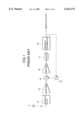
- FIG. 1 shows an example of a conventional automatic frequency circuit of an FM receiver.
- the FM receiver comprises an antenna 41 for receiving a radio wave transmitted from the transmitter side, a bandpass filter 42 for extracting a signal having a necessary band from the received signal, an amplifier 43 for amplifying the level of the signal passing through the bandpass filter 2 to a necessary level, a mixer 44 for decreasing the frequency of the received signal to a necessary frequency, an oscillator 45 for generating a necessary frequency, an amplifier 46 for amplifying the level of the received signal to a necessary level, a limiter 47 for limiting the amplitude of the received signal, and a frequency discriminator 48 for demodulating the received signal.
- a signal received by the antenna 41 is amplified by the amplifier 43, it is changed by the mixer 44 to a signal having a necessary frequency, amplified by the amplifier 46, limited in amplitude by the limiter 47, and demodulated by the frequency discriminator 48.
- the DC component of the demodulated data changes its polarity to positive or negative depending on the offset direction of the center frequency from the center of the S-mode characteristic of the discriminator. This DC component is negatively fed back to control the frequency of the oscillator.
- the present invention has been made in consideration of the above situation, and has as its object to enable correction of the influence of frequency offset even in the frequency selection multi-path fading environment in a radio data communication terminal of a scheme in which transmission path characteristics are obtained during the preamble period by narrow-band modulation to equalize the received signal.
- an automatic frequency control circuit for correcting influence of a frequency offset of a radio data communication terminal of a scheme in which a transmission path characteristic is obtained during a preamble period by narrow-band modulation to equalize a received signal, comprising on a transmitter side, means for repeatedly transmitting a pattern of a predetermined pseudo noise (PN) signal serving as a preamble signal; on a receiver side, means for calculating a phase difference per PN cycle on the basis of a component (real and imaginary part amplitude values) of a PN signal one cycle before that is quadrature-modulated during a predetermined period of the preamble, and a component of a current PN signal; means for dividing the phase difference by the number of symbols of one PN cycle to obtain a phase difference ( ⁇ ) of a unit symbol; means for holding ⁇ during a burst period; means for integrating ⁇ in units of symbols during data demodulation; means for converting an integrated value into
- PN pseudo noise
- an automatic frequency control circuit wherein, when a signal component has a level not more than a predetermined level, the means, defined in the first aspect, of calculating the phase difference per symbol on the basis of the component (real and imaginary part amplitude values) of the PN signal one cycle before that is quadrature-modulated during the predetermined period of the preamble, and the component of the current PN signal does not integrate the value.
- phase correction can be done in units of symbols during data demodulation by repeatedly transmitting the pattern of a predetermined PN signal serving as a preamble pattern from the transmitter side, and calculating the phase difference per PN cycle on the basis of the component of a PN signal one cycle before that is quadrature-modulated during a preamble period, and the component of the current PN signal on the receiver side. Therefore, automatic frequency control can be attained even in the frequency selection multi-path fading environment.
- phase correction can be done in units of symbols even in the frequency selection multi-path fading environment in automatic frequency control of correcting the influence of frequency offset in a radio data communication terminal of a scheme in which transmission path characteristics are obtained during the preamble period by narrow-band modulation to equalize the received signal. Accordingly, high-speed data communication can be realized even with a low-precision synthesizer, oscillator, or the like, and the apparatus can be downsized.
- FIG. 1 is a block diagram showing the arrangement of a conventional automatic frequency control circuit
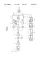
- FIG. 2 is a block diagram showing the whole arrangement of an embodiment of the present invention.
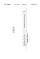
- FIG. 3 is a view showing the signal format of the transmission frame in the embodiment of the present invention.
- FIG. 4 is a block diagram showing a phase rotation unit, a phase difference detection circuit, an average value detection circuit, an integration circuit, and a vector conversion circuit shown in FIG. 2 in detail.
- FIG. 2 shows an example of the arrangement of automatic frequency control using a PN signal according to the present invention.
- a receiver comprises an antenna 1 for receiving a radio wave transmitted from the transmitter side (not shown), a bandpass filter 2 for extracting a signal having a necessary band from the received signal, an amplifier 3 for amplifying the level of the signal passing through the bandpass filter 2 to a necessary level, a mixer 4 for decreasing the frequency of the received signal to a necessary frequency, an oscillator 5 for generating a necessary frequency, an amplifier 6 for amplifying the level of the received signal to a necessary level, mixers 7 and 8, a 0°/90° phase generator 9, and an oscillator 10 which are used to quadrature-modulate the received signal, A/D converters 11 and 12 for A/D-converting the signals of quadrature-modulated real and imaginary part amplitude values, a phase rotation unit 13 for rotating the phase of the received signal by a necessary phase amount, a phase difference detection circuit 14 for obtaining the current angle and an angle after one
- FIG. 3 shows a transmission frame format in the embodiment of the present invention.
- This format is constituted by a preamble period in which frame synchronization detection or the like is performed, and an information data period.
- the same PN signal pattern is repeatedly transmitted during the preamble period.
- a phase difference between samples separated by one PN cycle is divided by the number of symbols of one PN cycle to obtain the phase difference ⁇ of the unit symbol, this value is held during one burst, and the value ⁇ is integrated in units of symbols to correct the phase of the incoming signal on the reception side.
- the receiver side receives a transmitted signal through the antenna 1.
- the phase difference detection circuit 14 obtains the current angle by using quadrature-modulated output signals from the A/D converters 11 and 12, and real and imaginary part amplitude values with reference to a table.
- the phase difference detection circuit 14 calculates the difference between the current angle and the angle obtained from the received signal one PN cycle before. This operation is repeatedly executed to input a predetermined number of differences to the average value detection circuit 15, and calculate the average value, which is performed for smoothing.
- the average value obtained, ⁇ is fixed during the burst period.
- the integration circuit 16 integrates ⁇ in units of symbols.
- the vector conversion circuit 17 converts the integrated value into a real part amplitude value and an imaginary part amplitude value, which are input to the phase rotation unit 13, and synthesized with the received signal to correct its phase.
- phase rotation unit 13 the phase difference detection circuit 14, the average value detection circuit 15, the integration circuit 16, and the vector conversion circuit 17 shown in FIG. 2 will be described in detail with reference to FIG. 4.
- the phase rotation unit 13 is built from multipliers 21, 22, 23, and 24, and adders 25 and 26.
- the phase difference detection circuit 14 is made up of an absolute value detection circuit 27, a comparison circuit 28, an angle detection unit 29, a delay circuit 30, a subtracter 31, and a signal switching circuit 32.
- the average value detection circuit 15 has an adder 33, a latch circuit 34, a divider 35, and a latch circuit 36, and the integration circuit 16 an adder 37 and a latch circuit 38.
- the vector conversion circuit 17 is constituted by a real part amplitude value detection circuit 39 and an imaginary part amplitude value detection circuit 40.
- the phase rotation unit 13 rotates the phase of the incoming signal by a necessary phase amount in combination with the multipliers 21, 22, 23, and 24 and the adders 25 and 26 in accordance with the addition theorem, thereby controlling the frequency of the signal.
- the absolute value detection circuit 27 inputs the amplitude values of the real and imaginary parts to the angle detection unit 29 to obtain an angle, and inputs the obtained value to the delay circuit 30 to delay the value by one cycle.
- the subtracter 31 calculates the difference between the angle value delayed by one cycle and the current angle value. At this time, when a signal of low level due to noise or the like is input, a correct phase difference cannot be calculated. For this reason, the absolute value detection circuit 27 calculates the absolute values of the amplitude values of the real and imaginary parts, and when the comparison circuit 28 determines that the signal level is equal to or lower than a predetermined level, the signal switching circuit 32 cancels the signal.
- the adder 33 adds a predetermined number of phase difference values, and the latch circuit 34 latches the added value.
- the divider 35 divides the latched value to obtain the average value, and the latch circuit 36 latches and holds the average value.
- the integration circuit 16 integrates the average value with the adder 37 and the latch circuit 38 to output a phase value.
- the phase value is input to the real part amplitude value detection circuit 39 and the imaginary part amplitude value detection circuit 40 to obtain the amplitude values of the real and imaginary parts, which are input to the phase rotation unit 13 to rotate the phase by a necessary phase amount and correct the phase.
Landscapes
- Engineering & Computer Science (AREA)
- Computer Networks & Wireless Communication (AREA)
- Signal Processing (AREA)
- Digital Transmission Methods That Use Modulated Carrier Waves (AREA)
- Channel Selection Circuits, Automatic Tuning Circuits (AREA)
Abstract
Description
Claims (2)
Applications Claiming Priority (2)
| Application Number | Priority Date | Filing Date | Title |
|---|---|---|---|
| JP8315904A JP2959498B2 (en) | 1996-11-27 | 1996-11-27 | Automatic frequency control circuit |
| JP8-315904 | 1996-11-27 |
Publications (1)
| Publication Number | Publication Date |
|---|---|
| US6151371A true US6151371A (en) | 2000-11-21 |
Family
ID=18071013
Family Applications (1)
| Application Number | Title | Priority Date | Filing Date |
|---|---|---|---|
| US08/976,777 Expired - Lifetime US6151371A (en) | 1996-11-27 | 1997-11-24 | Automatic frequency control circuit |
Country Status (2)
| Country | Link |
|---|---|
| US (1) | US6151371A (en) |
| JP (1) | JP2959498B2 (en) |
Cited By (6)
| Publication number | Priority date | Publication date | Assignee | Title |
|---|---|---|---|---|
| US6396884B1 (en) * | 1998-08-18 | 2002-05-28 | Nec Corporation | Automatic frequency control circuit |
| US6522702B1 (en) * | 1998-04-22 | 2003-02-18 | Nec Corporation | Radio data communication terminal |
| WO2002060144A3 (en) * | 2001-01-09 | 2003-02-20 | Qualcomm Inc | Calibrating the local oscillation frequency of a cdma receiver |
| US6661851B1 (en) * | 2000-10-20 | 2003-12-09 | Qualcomm Incorporated | Bi-directional vector rotator |
| US20130163572A1 (en) * | 2010-08-23 | 2013-06-27 | Electronics And Telecommunications Research Institute | Communication method using a preamble to share characteristic information, method for generating the preamble, and communication system to which the methods are applied |
| CN111181885A (en) * | 2018-11-13 | 2020-05-19 | 中国科学院上海高等研究院 | Transmission method and reception method of preamble signal in ultra-high-speed mobile broadband communication |
Families Citing this family (4)
| Publication number | Priority date | Publication date | Assignee | Title |
|---|---|---|---|---|
| JP2000032069A (en) | 1998-07-08 | 2000-01-28 | Nec Corp | Packet configuration method and packet receiver |
| JP3866908B2 (en) | 2000-07-31 | 2007-01-10 | 三菱電機株式会社 | Wireless communication receiver |
| JP4570558B2 (en) * | 2005-12-13 | 2010-10-27 | パナソニック株式会社 | Wireless communication apparatus and frequency offset amount estimation method |
| JP2011259091A (en) * | 2010-06-07 | 2011-12-22 | Sony Corp | Signal transmission system, signal processor, reference signal transmitter, reference signal receiver, electronic apparatus, signal transmission method |
Citations (3)
| Publication number | Priority date | Publication date | Assignee | Title |
|---|---|---|---|---|
| US5400366A (en) * | 1992-07-09 | 1995-03-21 | Fujitsu Limited | Quasi-synchronous detection and demodulation circuit and frequency discriminator used for the same |
| US5579346A (en) * | 1994-01-19 | 1996-11-26 | Kabushiki Kaisha Toshiba | Automatic frequency control method and circuit for use in a delay detection type demodulator |
| US5696797A (en) * | 1994-07-22 | 1997-12-09 | Motorola, Inc. | Demodulator with baseband doppler shift compensation and method |
-
1996
- 1996-11-27 JP JP8315904A patent/JP2959498B2/en not_active Expired - Fee Related
-
1997
- 1997-11-24 US US08/976,777 patent/US6151371A/en not_active Expired - Lifetime
Patent Citations (3)
| Publication number | Priority date | Publication date | Assignee | Title |
|---|---|---|---|---|
| US5400366A (en) * | 1992-07-09 | 1995-03-21 | Fujitsu Limited | Quasi-synchronous detection and demodulation circuit and frequency discriminator used for the same |
| US5579346A (en) * | 1994-01-19 | 1996-11-26 | Kabushiki Kaisha Toshiba | Automatic frequency control method and circuit for use in a delay detection type demodulator |
| US5696797A (en) * | 1994-07-22 | 1997-12-09 | Motorola, Inc. | Demodulator with baseband doppler shift compensation and method |
Cited By (8)
| Publication number | Priority date | Publication date | Assignee | Title |
|---|---|---|---|---|
| US6522702B1 (en) * | 1998-04-22 | 2003-02-18 | Nec Corporation | Radio data communication terminal |
| US6396884B1 (en) * | 1998-08-18 | 2002-05-28 | Nec Corporation | Automatic frequency control circuit |
| US6661851B1 (en) * | 2000-10-20 | 2003-12-09 | Qualcomm Incorporated | Bi-directional vector rotator |
| WO2002060144A3 (en) * | 2001-01-09 | 2003-02-20 | Qualcomm Inc | Calibrating the local oscillation frequency of a cdma receiver |
| US20130163572A1 (en) * | 2010-08-23 | 2013-06-27 | Electronics And Telecommunications Research Institute | Communication method using a preamble to share characteristic information, method for generating the preamble, and communication system to which the methods are applied |
| US8995409B2 (en) * | 2010-08-23 | 2015-03-31 | Electronics And Telecommunications Research Institute | Communication method using a preamble to share characteristic information, method for generating the preamble, and communication system to which the methods are applied |
| CN111181885A (en) * | 2018-11-13 | 2020-05-19 | 中国科学院上海高等研究院 | Transmission method and reception method of preamble signal in ultra-high-speed mobile broadband communication |
| CN111181885B (en) * | 2018-11-13 | 2022-09-09 | 中国科学院上海高等研究院 | Transmission method and reception method of preamble signal in ultra-high-speed mobile broadband communication |
Also Published As
| Publication number | Publication date |
|---|---|
| JPH10163816A (en) | 1998-06-19 |
| JP2959498B2 (en) | 1999-10-06 |
Similar Documents
| Publication | Publication Date | Title |
|---|---|---|
| JP3744546B2 (en) | Variable of sampled signal C. Method and apparatus for compensating offset | |
| US5610946A (en) | Radio communication apparatus | |
| EP1391997B1 (en) | Digitally compensated direct conversion receiver | |
| US4977580A (en) | Timing and carrier recovery in TDMA without preamble sequence | |
| US7200188B2 (en) | Method and apparatus for frequency offset compensation | |
| KR100780117B1 (en) | Angular Modulated Rf Signal Receiver | |
| US6133964A (en) | Digital demodulator and method therefor | |
| JPH0758928B2 (en) | Method and circuit device for receiving frequency-modulated radio wave | |
| JPH04502241A (en) | Method and apparatus for demodulating orthogonally modulated signals | |
| US20100261434A1 (en) | Phase noise correction circuit, transmission device,reception device, radio device, radio communication system, and phase noise correction method | |
| EP0381637B1 (en) | A method of controlling the frequency of a coherent radio receiver and apparatus for carrying out the method | |
| US6151371A (en) | Automatic frequency control circuit | |
| EP1209872B1 (en) | Frequency control in a PSK receiver | |
| US6396884B1 (en) | Automatic frequency control circuit | |
| US20160226686A1 (en) | Receiving apparatus and receiving method | |
| US5373247A (en) | Automatic frequency control method and circuit for correcting an error between a received carrier frequency and a local frequency | |
| US20060062331A1 (en) | Demodulator for use in wireless communications and receiver, method and terminal using it | |
| JP3383318B2 (en) | Digital modulation wave demodulator | |
| US6914946B1 (en) | Digitally-implemented demodulator | |
| US6243429B1 (en) | Data demodulator for correcting bit errors | |
| JP2000004264A (en) | SN ratio estimating circuit and receiving device | |
| JPH0823361A (en) | TDMA data receiver | |
| CA2262941A1 (en) | Demodulator with digital circuit for recovering carrier and rhythm | |
| MXPA97004753A (en) | Receiver of direct conversion, compensated digitalme |
Legal Events
| Date | Code | Title | Description |
|---|---|---|---|
| AS | Assignment |
Owner name: NEC CORPORATION, A CORP, OF JAPAN, JAPAN Free format text: ASSIGNMENT OF ASSIGNORS INTEREST;ASSIGNOR:MARUYAMA, HIDENORI;REEL/FRAME:008956/0707 Effective date: 19971114 |
|
| STCF | Information on status: patent grant |
Free format text: PATENTED CASE |
|
| FEPP | Fee payment procedure |
Free format text: PAYOR NUMBER ASSIGNED (ORIGINAL EVENT CODE: ASPN); ENTITY STATUS OF PATENT OWNER: LARGE ENTITY |
|
| FPAY | Fee payment |
Year of fee payment: 4 |
|
| FPAY | Fee payment |
Year of fee payment: 8 |
|
| FPAY | Fee payment |
Year of fee payment: 12 |
|
| AS | Assignment |
Owner name: RAKUTEN, INC., JAPAN Free format text: ASSIGNMENT OF ASSIGNORS INTEREST;ASSIGNOR:NEC CORPORATION;REEL/FRAME:028252/0280 Effective date: 20120514 |
|
| AS | Assignment |
Owner name: RAKUTEN, INC., JAPAN Free format text: CHANGE OF ADDRESS;ASSIGNOR:RAKUTEN, INC.;REEL/FRAME:037751/0006 Effective date: 20150824 |