US6150267A - Method of manufacturing buried contact in SRAM - Google Patents
Method of manufacturing buried contact in SRAM Download PDFInfo
- Publication number
- US6150267A US6150267A US09/185,915 US18591598A US6150267A US 6150267 A US6150267 A US 6150267A US 18591598 A US18591598 A US 18591598A US 6150267 A US6150267 A US 6150267A
- Authority
- US
- United States
- Prior art keywords
- substrate
- contact window
- forming
- conductive layer
- opening
- Prior art date
- Legal status (The legal status is an assumption and is not a legal conclusion. Google has not performed a legal analysis and makes no representation as to the accuracy of the status listed.)
- Expired - Fee Related
Links
Images

Classifications
-
- H10W20/0698—
Definitions
- the present invention relates to a method of manufacturing static random access memory (SRAM). More particularly, the present invention relates to a method of manufacturing a buried contact in an SRAM.
- SRAM static random access memory
- SRAM is one of the fastest operating semiconductor memory devices. Therefore, SRAM has been widely used, for example, in the cache memory of a computer. At present, SRAMs are also used in microcomputers, microprocessors and other digital equipment.
- an SRAM integrated circuit can be divided into two regions, namely, a memory cell region and a peripheral circuit region.
- the memory cell region comprises a large number of memory cell units, each for storing a single bit of data.
- the peripheral circuit region includes some address decoders for decoding the memory addresses coming from the memory cell region and some memory operating circuits.
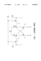
- FIG. 1 is a circuit diagram of a memory unit in the memory cell region of SRAM.
- an SRAM cell comprises resistors R 1 and R 2 and MOS transistors T 1 , T 2 , T 3 and T 4 .
- the resistor R 1 is connected in series with the MOS transistor T 1 , while the drain and the source of the MOS transistor T 1 are connected to the voltage source V DD and ground V SS , respectively.
- the resistor R 2 is connected in series with the MOS transistor T 2 , while the drain and the source of the MOS transistor T 2 are connected to the voltage source V DD and ground V SS , respectively.
- the gate of the MOS transistor T 2 , the drain of MOS transistor T 1 and the drain of MOS transistor T 3 are connected at node point A.
- the gate of the MOS transistor T 1 , the drain of MOS transistor T 2 and the drain of MOS transistor T 4 are connected at node point B.
- the gates of the MOS transistors T 3 and T 4 are connected to a word line WL, while the sources of the MOS transistor T 3 and T 4 are connected to the bit line BL and the complementary bit line BL, respectively.
- Transistors T 1 and T 2 act as drivers, and transistors T 3 and T 4 act as a relays for accessing data.
- the resistor elements R 1 and R 2 serve as loads.
- the contact windows of conventional SRAM are formed mostly above the source/drain regions.
- the conventional method of forming contact windows becomes infeasible. Therefore, a type of contact window known as a buried contact window, which is especially suitable for forming local interconnects, is developed.
- a buried contact window is capable of reducing wafer occupation. For example, when a buried contact is formed in an SRAM unit, as much as 25% of chip area can be saved. Hence, buried contact windows are preferred in high-density semiconductor products.
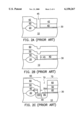
- FIGS. 2A through 2C are schematic, cross-sectional views showing the progression of steps in producing a buried contact window in SRAM according to the conventional method.
- a semiconductor substrate 10 is provided.
- a device isolation structure for example, a field oxide (FOX) layer 20 is formed above the substrate 10.
- a gate oxide layer 30 is formed over the substrate 10, and then a first polysilicon layer 40 is deposited over the gate oxide layer 30.
- a photoresist layer 42 is coated over the first polysilicon layer 40, and then the photoresist layer 42 is patterned.
- the first polysilicon layer 40 and the gate oxide layer 30 are sequentially etched, thereby forming a buried contact window opening 45.
- the photoresist layer 42 is removed.
- a second polysilicon layer 50 and a tungsten suicide layer 60 are sequentially formed over the first polysilicon layer 40 and the buried contact window opening 45.
- FIG. 2C conventional photolithographic technique is used to pattern out the source/drain region.
- the tungsten silicide layer 60 and the second polysilicon layer 50 are sequentially etched to form a conductive line 65 and a gate 75. Therefore, between the conductive line 65 and the gate 75, an opening 70 that exposes the surface of the source/drain region 90 is also formed.
- the opening 70 is purposely formed in a position slightly shifted towards the field oxide layer 20.
- a trench 80 as shown in FIG. 2C is also formed in the substrate 10.
- thickness of the gate oxide layer 30d underneath the opening 70 is also reduced due to etching.
- ions are implanted into the substrate at the bottom of the opening 70 using the tungsten silicide layer 60 as a mask, thereby forming doped regions 90 and 100 in the substrate. Since the ions need not strike the substrate perpendicularly, and a trench 80 was formed in a previous etching operation, some ions are trapped in the buried contact window 100 on the left side at the bottom of the opening 70 and next to the source/drain region 90.
- a trench 80 is also formed. If the depth of this trench 80 is great, contact area between the buried contact window 100 and the source/drain region 90 will be small. Hence, resistance at the junction increases considerably. Moreover, if the depth of the trench 80 is too deep, there may be a re-direction of current. Instead of passing through the implanted regions 90 and 100, the current flows by way of the substrate 10 and ground, thereby leading to junction leakage.
- the present invention provides a method of manufacturing the buried contact window of SRAM so that the depth of trench within the buried contact window is reduced, and junction leakage can be prevented as well.
- the invention provides a method of manufacturing a buried contact window in an SRAM.
- the method includes the steps of forming a gate oxide layer over a semiconductor substrate, and then forming a device isolation structure above the substrate. Thereafter, a first polysilicon layer is formed over the gate oxide layer. Then, photolithographic and etching operations are conducted to form a buried contact window opening in the first polysilicon layer and the gate oxide layer.
- the contact window opening is patterned again, and then oxygen ions are implanted into the substrate on one side of the desired source/drain location.
- a second polysilicon layer and a tungsten silicide layer are sequentially formed over the first polysilicon layer and the buried contact window opening. In the process of depositing the second polysilicon layer the high reaction temperature needed to deposit polysilicon is able to transform the oxygen ion implanted region into a silicon oxide layer
- the opening is located within the tungsten silicide layer and the second polysilicon layer on one side of the previously formed buried contact window opening. In other words, the opening is located between a gate and a conductive line. Since a patch of oxide is formed in the substrate on one side of the source/drain region, the etching selectivity ratio there is increased. Consequently, a trench having a depth less than the conventional depth is formed, thereby avoiding a high resistance at the junction between the buried contact window and the source/drain region or any junction leakage current.
- FIG. 1 is a circuit diagram of a memory unit in the memory cell region of SRAM
- FIGS. 2A through 2C are schematic, cross-sectional views showing the progression of steps in producing a buried contact window in SRAM according to the conventional method.
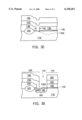
- FIGS. 3A through 3D are schematic, cross-sectional views showing the progression of steps in producing a buried contact window in SRAM according to one preferred embodiment of this invention.
- FIGS. 3A through 3D are schematic, cross-sectional views showing the progression of steps in producing a buried contact window in SRAM according to one preferred embodiment of this invention.
- a semiconductor substrate 110 is provided.
- a device isolation structure for example, a field oxide (FOX) layer 120 is formed above the substrate 110.
- a gate oxide layer 130 is formed over the substrate 110 using, for example, a thermal oxidation method.
- the gate oxide layer 130 can be a silicon oxide layer having a thickness of about 100 ⁇ to 250 ⁇ .
- a first polysilicon layer 140 is formed over the gate oxide layer 130.
- the first polysilicon layer 140 is deposited by heating to a temperature of between 575° C. to 650° C. using SiH 4 as the reactive gas in a low pressure chemical vapor deposition (LPCVD) process.
- LPCVD low pressure chemical vapor deposition
- a first layer of photoresist 142 is coated over the first polysilicon layer 140, and then the photoresist layer 142 is patterned.
- the first polysilicon layer 140 and the gate oxide layer 130 are etched to form a buried contact window opening 145.
- the photoresist layer 142 is removed.
- a second layer of photoresist 146 is coated over the first polysilicon layer 140. Then, the photoresist layer 146 is patterned to form a small opening 145a occupying only a portion of the buried contact window opening 145. The small opening 145a is formed on one side of the desired source/drain location. Thereafter, employing oxygen plasma 148, oxygen ions are implanted into the substrate region 135a through the opening 145a.
- the implanted oxygen ions in the region 135a are permitted to react with silicon to form a silicon oxide layer.
- the silicon oxide layer is used as a protective cover protecting against over-etching of the substrate to form a deep trench when an opening leading to the source/drain region is later formed.
- the implanted oxygen ions in the region 135a can react with silicon utilizing the high temperature of a subsequent polysilicon deposition.
- the region 135a can be exposed to a laser beam to hasten the reaction between silicon and oxygen to form a silicon oxide layer. It is of note that oxygen ions are implanted into the bottom of the opening 145a instead of the bottom of the whole buried contact window opening 145. This is because subsequently deposited conductive material can form a good electrical contact with the contact window surface only if there is an undoped region.
- the photoresist layer 146 is removed.
- a second polysilicon layer 150 and a tungsten silicide layer 160 are sequentially formed over the first polysilicon layer 140 and the buried contact window opening 145.
- the implanted oxygen ions in region 135a will be transformed into a local oxide region 135b after a laser beam is applied to that area, or when the second polysilicon layer 150 is deposited at a high temperature. Hence, a portion of the substrate surface is protected.
- the tungsten silicide is deposited over the second polysilicon layer using WF6 and SiH 4 as reactive gases at a temperature of between 300° C. to 400° C. in a LPCVD operation, for example.
- photolithographic and etching operations are carried out to form a conductive line 165 and a gate 175 within the tungsten suicide 160, the second polysilicon layer 150 and the first polysilicon layer 140.
- an opening 170 that leads to a source/drain region and a trench 180 in the substrate 110 are formed.
- the gate oxide layer 130d directly underneath the opening 170 is thinner than the gate oxide layer 130.
- depth of the trench 180 after the etching will be much shallower than a conventional trench.
- ion implantation is carried out using the tungsten silicide layer 160 as a mask to form the ion doped regions including a source/drain region 190 and a buried contact window 200 in the substrate 110.
- the major aspect of this invention includes performing an oxygen ion implant in a portion of the buried contact window opening. Then, using the heat in a subsequent polysilicon deposition operation or a laser beam, an oxidation reaction is initiated, thereby forming a protective oxide layer over the substrate. Therefore, when various overlying layers are etched to form an opening that leads directly to the source/drain region, the oxide layer can serve as a buffer region preventing the formation of a deep trench.
- the invention is capable of reducing the depth of trench located in the buried contact window region, and hence is able to reduce contact resistance between the buried contact window and the source/drain region or any leakage current at the junction.
Landscapes
- Semiconductor Memories (AREA)
- Electrodes Of Semiconductors (AREA)
Abstract
A method of manufacturing buried contact window in SRAM includes implanting oxygen ions into a substrate inside a buried contact window region adjacent to the location for forming a source/drain region, and then carrying out oxidative reaction in the implanted region to form an silicon oxide layer using the heat generated by a subsequent polysilicon deposition process or a laser beam. The silicon oxide layer protects the substrate by acting as a buffer, thus preventing the substrate from being over-etched to form a deep trench. Consequently, contact resistance between the buried contact window and the source/drain region is lowered, and leakage current at the junction is prevented.
Description
1. Field of Invention
The present invention relates to a method of manufacturing static random access memory (SRAM). More particularly, the present invention relates to a method of manufacturing a buried contact in an SRAM.
2. Description of Related Art
SRAM is one of the fastest operating semiconductor memory devices. Therefore, SRAM has been widely used, for example, in the cache memory of a computer. At present, SRAMs are also used in microcomputers, microprocessors and other digital equipment.
In general, an SRAM integrated circuit can be divided into two regions, namely, a memory cell region and a peripheral circuit region. The memory cell region comprises a large number of memory cell units, each for storing a single bit of data. The peripheral circuit region includes some address decoders for decoding the memory addresses coming from the memory cell region and some memory operating circuits. FIG. 1 is a circuit diagram of a memory unit in the memory cell region of SRAM.
As shown in FIG. 1, an SRAM cell comprises resistors R1 and R2 and MOS transistors T1, T2, T3 and T4. The resistor R1 is connected in series with the MOS transistor T1, while the drain and the source of the MOS transistor T1 are connected to the voltage source VDD and ground VSS, respectively. Similarly, The resistor R2 is connected in series with the MOS transistor T2, while the drain and the source of the MOS transistor T2 are connected to the voltage source VDD and ground VSS, respectively.
In addition, the gate of the MOS transistor T2, the drain of MOS transistor T1 and the drain of MOS transistor T3 are connected at node point A. Similarly, the gate of the MOS transistor T1, the drain of MOS transistor T2 and the drain of MOS transistor T4 are connected at node point B. The gates of the MOS transistors T3 and T4 are connected to a word line WL, while the sources of the MOS transistor T3 and T4 are connected to the bit line BL and the complementary bit line BL, respectively. Transistors T1 and T2 act as drivers, and transistors T3 and T4 act as a relays for accessing data. Lastly, the resistor elements R1 and R2 serve as loads.
In general, the contact windows of conventional SRAM are formed mostly above the source/drain regions. However, for integrated circuits having a high level of integration, the conventional method of forming contact windows becomes infeasible. Therefore, a type of contact window known as a buried contact window, which is especially suitable for forming local interconnects, is developed. A buried contact window is capable of reducing wafer occupation. For example, when a buried contact is formed in an SRAM unit, as much as 25% of chip area can be saved. Hence, buried contact windows are preferred in high-density semiconductor products.
FIGS. 2A through 2C are schematic, cross-sectional views showing the progression of steps in producing a buried contact window in SRAM according to the conventional method.
First, as shown in FIG. 2A, a semiconductor substrate 10 is provided. Then, a device isolation structure, for example, a field oxide (FOX) layer 20 is formed above the substrate 10. Next, a gate oxide layer 30 is formed over the substrate 10, and then a first polysilicon layer 40 is deposited over the gate oxide layer 30. Thereafter, a photoresist layer 42 is coated over the first polysilicon layer 40, and then the photoresist layer 42 is patterned. In the subsequent step, the first polysilicon layer 40 and the gate oxide layer 30 are sequentially etched, thereby forming a buried contact window opening 45.
Next, as shown in FIG. 2B, the photoresist layer 42 is removed. Then, a second polysilicon layer 50 and a tungsten suicide layer 60 are sequentially formed over the first polysilicon layer 40 and the buried contact window opening 45.
Next, as shown in FIG. 2C, conventional photolithographic technique is used to pattern out the source/drain region. Thereafter, the tungsten silicide layer 60 and the second polysilicon layer 50 are sequentially etched to form a conductive line 65 and a gate 75. Therefore, between the conductive line 65 and the gate 75, an opening 70 that exposes the surface of the source/drain region 90 is also formed. The opening 70 is purposely formed in a position slightly shifted towards the field oxide layer 20. Furthermore, since the second polysilicon layer 50 and the substrate 10 are made from the same material, a trench 80 as shown in FIG. 2C is also formed in the substrate 10. In addition, thickness of the gate oxide layer 30d underneath the opening 70 is also reduced due to etching.
Thereafter, ions are implanted into the substrate at the bottom of the opening 70 using the tungsten silicide layer 60 as a mask, thereby forming doped regions 90 and 100 in the substrate. Since the ions need not strike the substrate perpendicularly, and a trench 80 was formed in a previous etching operation, some ions are trapped in the buried contact window 100 on the left side at the bottom of the opening 70 and next to the source/drain region 90.
In the aforementioned method of forming an opening 70 to the source/drain region 90, a trench 80 is also formed. If the depth of this trench 80 is great, contact area between the buried contact window 100 and the source/drain region 90 will be small. Hence, resistance at the junction increases considerably. Moreover, if the depth of the trench 80 is too deep, there may be a re-direction of current. Instead of passing through the implanted regions 90 and 100, the current flows by way of the substrate 10 and ground, thereby leading to junction leakage.
In light of the foregoing, there is a need a more efficient method of fabrication buried contact window in SRAM.
Accordingly, the present invention provides a method of manufacturing the buried contact window of SRAM so that the depth of trench within the buried contact window is reduced, and junction leakage can be prevented as well.
To achieve these and other advantages and in accordance with the purpose of the invention, as embodied and broadly described herein, the invention provides a method of manufacturing a buried contact window in an SRAM. The method includes the steps of forming a gate oxide layer over a semiconductor substrate, and then forming a device isolation structure above the substrate. Thereafter, a first polysilicon layer is formed over the gate oxide layer. Then, photolithographic and etching operations are conducted to form a buried contact window opening in the first polysilicon layer and the gate oxide layer.
Next, the contact window opening is patterned again, and then oxygen ions are implanted into the substrate on one side of the desired source/drain location. A second polysilicon layer and a tungsten silicide layer are sequentially formed over the first polysilicon layer and the buried contact window opening. In the process of depositing the second polysilicon layer the high reaction temperature needed to deposit polysilicon is able to transform the oxygen ion implanted region into a silicon oxide layer
Thereafter, photolithographic and etching operations are again carried out to form an opening leading to the source/drain region. The opening is located within the tungsten silicide layer and the second polysilicon layer on one side of the previously formed buried contact window opening. In other words, the opening is located between a gate and a conductive line. Since a patch of oxide is formed in the substrate on one side of the source/drain region, the etching selectivity ratio there is increased. Consequently, a trench having a depth less than the conventional depth is formed, thereby avoiding a high resistance at the junction between the buried contact window and the source/drain region or any junction leakage current.
It is to be understood that both the foregoing general description and the following detailed description are exemplary, and are intended to provide further explanation of the invention as claimed.
The accompanying drawings are included to provide a further understanding of the invention, and are incorporated in and constitute a part of this specification. The drawings illustrate embodiments of the invention and, together with the description, serve to explain the principles of the invention. In the drawings,
FIG. 1 is a circuit diagram of a memory unit in the memory cell region of SRAM;
FIGS. 2A through 2C are schematic, cross-sectional views showing the progression of steps in producing a buried contact window in SRAM according to the conventional method; and
FIGS. 3A through 3D are schematic, cross-sectional views showing the progression of steps in producing a buried contact window in SRAM according to one preferred embodiment of this invention.
Reference will now be made in detail to the present preferred embodiments of the invention, examples of which are illustrated in the accompanying drawings. Wherever possible, the same reference numbers are used in the drawings and the description to refer to the same or like parts.
FIGS. 3A through 3D are schematic, cross-sectional views showing the progression of steps in producing a buried contact window in SRAM according to one preferred embodiment of this invention.
As shown in FIG. 3A, a semiconductor substrate 110 is provided. A device isolation structure, for example, a field oxide (FOX) layer 120 is formed above the substrate 110. Thereafter, a gate oxide layer 130 is formed over the substrate 110 using, for example, a thermal oxidation method. The gate oxide layer 130 can be a silicon oxide layer having a thickness of about 100 Å to 250 Å.
In the subsequent step, a first polysilicon layer 140 is formed over the gate oxide layer 130. For example, the first polysilicon layer 140 is deposited by heating to a temperature of between 575° C. to 650° C. using SiH4 as the reactive gas in a low pressure chemical vapor deposition (LPCVD) process. After that, a first layer of photoresist 142 is coated over the first polysilicon layer 140, and then the photoresist layer 142 is patterned. Subsequently, the first polysilicon layer 140 and the gate oxide layer 130 are etched to form a buried contact window opening 145. Finally, the photoresist layer 142 is removed.
As shown in FIG. 3B, a second layer of photoresist 146 is coated over the first polysilicon layer 140. Then, the photoresist layer 146 is patterned to form a small opening 145a occupying only a portion of the buried contact window opening 145. The small opening 145a is formed on one side of the desired source/drain location. Thereafter, employing oxygen plasma 148, oxygen ions are implanted into the substrate region 135a through the opening 145a.
The implanted oxygen ions in the region 135a are permitted to react with silicon to form a silicon oxide layer. The silicon oxide layer is used as a protective cover protecting against over-etching of the substrate to form a deep trench when an opening leading to the source/drain region is later formed. The implanted oxygen ions in the region 135a can react with silicon utilizing the high temperature of a subsequent polysilicon deposition.
Alternatively, the region 135a can be exposed to a laser beam to hasten the reaction between silicon and oxygen to form a silicon oxide layer. It is of note that oxygen ions are implanted into the bottom of the opening 145a instead of the bottom of the whole buried contact window opening 145. This is because subsequently deposited conductive material can form a good electrical contact with the contact window surface only if there is an undoped region.
As shown in FIG. 3C, the photoresist layer 146 is removed. After that, a second polysilicon layer 150 and a tungsten silicide layer 160 are sequentially formed over the first polysilicon layer 140 and the buried contact window opening 145. The implanted oxygen ions in region 135a will be transformed into a local oxide region 135b after a laser beam is applied to that area, or when the second polysilicon layer 150 is deposited at a high temperature. Hence, a portion of the substrate surface is protected. The tungsten silicide is deposited over the second polysilicon layer using WF6 and SiH4 as reactive gases at a temperature of between 300° C. to 400° C. in a LPCVD operation, for example.
As shown in FIG. 3D, photolithographic and etching operations are carried out to form a conductive line 165 and a gate 175 within the tungsten suicide 160, the second polysilicon layer 150 and the first polysilicon layer 140. Between the conductive line 165 and the gate 175, an opening 170 that leads to a source/drain region and a trench 180 in the substrate 110 are formed. Because of etching, the gate oxide layer 130d directly underneath the opening 170 is thinner than the gate oxide layer 130. However, due to the presence of a protective oxide in region 135b above the substrate 110, depth of the trench 180 after the etching will be much shallower than a conventional trench. In the subsequent step, ion implantation is carried out using the tungsten silicide layer 160 as a mask to form the ion doped regions including a source/drain region 190 and a buried contact window 200 in the substrate 110.
In summary, the major aspect of this invention includes performing an oxygen ion implant in a portion of the buried contact window opening. Then, using the heat in a subsequent polysilicon deposition operation or a laser beam, an oxidation reaction is initiated, thereby forming a protective oxide layer over the substrate. Therefore, when various overlying layers are etched to form an opening that leads directly to the source/drain region, the oxide layer can serve as a buffer region preventing the formation of a deep trench.
Therefore, the invention is capable of reducing the depth of trench located in the buried contact window region, and hence is able to reduce contact resistance between the buried contact window and the source/drain region or any leakage current at the junction.
It will be apparent to those skilled in the art that various modifications and variations can be made to the structure of the present invention without departing from the scope or spirit of the invention. In view of the foregoing, it is intended that the present invention cover modifications and variations of this invention provided they fall within the scope of the following claims and their equivalents.
Claims (19)
1. A method of manufacturing a buried contact window of an SRAM, comprising the steps of:
providing a substrate, wherein the substrate has a device isolation structure;
forming an oxide layer and a first conductive layer over the substrate;
patterning the first conductive layer to form a first opening in a buried contact window region, wherein the first opening exposes the substrate in the buried contact window region;
patterning an area within the buried contact window region adjacent to one side of a desired source/drain region, and then performing a first ion implantation in that area;
forming a second conductive layer, wherein the second conductive layer connects electrically with the substrate through the first opening;
patterning the second conductive layer to form a conductive line and a gate together with a second opening between the conductive line and the gate such that the second opening exposes the desired source/drain region and a portion of the buried ion-doped contact window region; and
performing a second ion implantation implanting ions into the substrate through the second opening to form a buried contact window and a source/drain region.
2. The method of claim 1, wherein the step of forming the first conductive layer includes depositing polysilicon to form a polysilicon layer.
3. The method of claim 2, wherein the step of forming the polysilicon layer includes low pressure chemical vapor deposition using SiH4 as gaseous reactant at a temperature of roughly between 575° C. to 650° C.
4. The method of claim 1, wherein the step of forming the second conductive layer includes depositing polysilicon and tungsten silicide.
5. The method of claim 4, wherein the step of forming the polysilicon layer includes low pressure chemical vapor deposition using SiH4 as gaseous reactant at a temperature of roughly between 575° C. to 650° C.
6. The method of claim 4, wherein the step of forming the tungsten silicide layer includes low pressure chemical vapor deposition using WF6 and SiH4 as gaseous reactants at a temperature of roughly between 300° C. to 400° C.
7. The method of claim 1, wherein the first ion implantation includes implanting oxygen ions.
8. The method of claim 7, wherein after the step of implanting oxygen ions into the substrate, further includes using a laser beam to heat the implanted region locally so that the oxygen ions can react with silicon to form a silicon oxide layer.
9. The method of claim 7, wherein after the step of implanting oxygen ions into the substrate, further includes using the heat generated during the deposition of the second conductive layer to activate the reaction between the implanted oxygen ions and silicon for the production of a silicon oxide layer.
10. A method of manufacturing a buried contact window of an SRAM, comprising the steps of:
providing a substrate, wherein the substrate has a device isolation structure;
forming an oxide layer and a first conductive layer over the substrate;
patterning the first conductive layer to form a first opening in a buried contact window region, wherein the first opening exposes the substrate in the buried contact window region;
patterning an area within the buried contact window region located to one side of a desired source/drain region, and then performing a first ion implantation in that area;
forming a second conductive layer, wherein the second conductive layer connects electrically with the substrate through the first opening;
patterning the second conductive layer to form a conductive line and a gate together with a second opening located between the conductive line and the gate such that the second opening exposes the desired source/drain region and a portion of the buried ion-doped contact window region.
11. The method of claim 10, wherein the step of forming the first conductive layer includes depositing polysilicon to form a polysilicon layer.
12. The method of claim 1, wherein the step of forming the polysilicon layer includes low pressure chemical vapor deposition using SiH4 as gaseous reactant at a temperature of roughly between 575° C. to 650° C.
13. The method of claim 10, wherein the step of forming the second conductive layer includes depositing polysilicon and tungsten silicide.
14. The method of claim 13, wherein the step of forming the polysilicon layer includes low pressure chemical vapor deposition using SiH4 as gaseous reactant at a temperature of roughly between 575° C. to 650° C.
15. The method of claim 13, wherein the step of forming the tungsten silicide layer includes low pressure chemical vapor deposition using WF6 and SiH4 as gaseous reactants at a temperature of roughly between 300° C. to 400° C.
16. The method of claim 10, wherein the first ion implantation includes implanting oxygen ions.
17. The method of claim 16, wherein after the step of implanting oxygen ions into the substrate, further includes using a laser beam to heat the implanted region locally so that the oxygen ions can react with silicon to form a silicon oxide layer.
18. The method of claim 16, wherein after the step of implanting oxygen ions into the substrate, further includes using the heat generated during the deposition of the second conductive layer to activate the reaction between the implanted oxygen ions and silicon for the production of a silicon oxide layer.
19. The method of claim 10, wherein after the step of forming the second opening, further includes the steps of performing a second ion implantation implanting ions into the substrate through the second opening to form a buried contact window and a source/drain region.
Priority Applications (1)
| Application Number | Priority Date | Filing Date | Title |
|---|---|---|---|
| US09/185,915 US6150267A (en) | 1998-11-04 | 1998-11-04 | Method of manufacturing buried contact in SRAM |
Applications Claiming Priority (1)
| Application Number | Priority Date | Filing Date | Title |
|---|---|---|---|
| US09/185,915 US6150267A (en) | 1998-11-04 | 1998-11-04 | Method of manufacturing buried contact in SRAM |
Publications (1)
| Publication Number | Publication Date |
|---|---|
| US6150267A true US6150267A (en) | 2000-11-21 |
Family
ID=22682947
Family Applications (1)
| Application Number | Title | Priority Date | Filing Date |
|---|---|---|---|
| US09/185,915 Expired - Fee Related US6150267A (en) | 1998-11-04 | 1998-11-04 | Method of manufacturing buried contact in SRAM |
Country Status (1)
| Country | Link |
|---|---|
| US (1) | US6150267A (en) |
Cited By (3)
| Publication number | Priority date | Publication date | Assignee | Title |
|---|---|---|---|---|
| US6440804B1 (en) * | 2001-07-24 | 2002-08-27 | United Microelectronics Corp. | Static random access memory manufacturing method |
| US20050056885A1 (en) * | 2003-09-15 | 2005-03-17 | Chih-Yang Pai | Dual poly layer and method of manufacture |
| US9287313B2 (en) | 2013-03-12 | 2016-03-15 | Taiwan Semiconductor Manufacturing Co., Ltd. | Active pixel sensor having a raised source/drain |
Citations (5)
| Publication number | Priority date | Publication date | Assignee | Title |
|---|---|---|---|---|
| US5525552A (en) * | 1995-06-08 | 1996-06-11 | Taiwan Semiconductor Manufacturing Company | Method for fabricating a MOSFET device with a buried contact |
| US5652152A (en) * | 1996-04-22 | 1997-07-29 | Chartered Semiconductor Manufacturing Pte, Ltd. | Process having high tolerance to buried contact mask misalignment by using a PSG spacer |
| US5728615A (en) * | 1996-07-18 | 1998-03-17 | Vanguard International Semiconductor Corporation | Method of manufacturing a polysilicon resistor having uniform resistance |
| US5751043A (en) * | 1994-07-25 | 1998-05-12 | Taiwan Semiconductor Manufacturing Company, Ltd. | SRAM with SIPOS resistor |
| US5894151A (en) * | 1992-02-25 | 1999-04-13 | Semiconductor Energy Laboratory Co., Ltd. | Semiconductor device having reduced leakage current |
-
1998
- 1998-11-04 US US09/185,915 patent/US6150267A/en not_active Expired - Fee Related
Patent Citations (5)
| Publication number | Priority date | Publication date | Assignee | Title |
|---|---|---|---|---|
| US5894151A (en) * | 1992-02-25 | 1999-04-13 | Semiconductor Energy Laboratory Co., Ltd. | Semiconductor device having reduced leakage current |
| US5751043A (en) * | 1994-07-25 | 1998-05-12 | Taiwan Semiconductor Manufacturing Company, Ltd. | SRAM with SIPOS resistor |
| US5525552A (en) * | 1995-06-08 | 1996-06-11 | Taiwan Semiconductor Manufacturing Company | Method for fabricating a MOSFET device with a buried contact |
| US5652152A (en) * | 1996-04-22 | 1997-07-29 | Chartered Semiconductor Manufacturing Pte, Ltd. | Process having high tolerance to buried contact mask misalignment by using a PSG spacer |
| US5728615A (en) * | 1996-07-18 | 1998-03-17 | Vanguard International Semiconductor Corporation | Method of manufacturing a polysilicon resistor having uniform resistance |
Cited By (6)
| Publication number | Priority date | Publication date | Assignee | Title |
|---|---|---|---|---|
| US6440804B1 (en) * | 2001-07-24 | 2002-08-27 | United Microelectronics Corp. | Static random access memory manufacturing method |
| US20050056885A1 (en) * | 2003-09-15 | 2005-03-17 | Chih-Yang Pai | Dual poly layer and method of manufacture |
| US7208369B2 (en) * | 2003-09-15 | 2007-04-24 | Taiwan Semiconductor Manufacturing Company, Ltd. | Dual poly layer and method of manufacture |
| US9287313B2 (en) | 2013-03-12 | 2016-03-15 | Taiwan Semiconductor Manufacturing Co., Ltd. | Active pixel sensor having a raised source/drain |
| US9397135B2 (en) | 2013-03-12 | 2016-07-19 | Taiwan Semiconductor Manufacturing Co., Ltd. | Active pixel sensor having a raised source/drain |
| US9985070B2 (en) | 2013-03-12 | 2018-05-29 | Taiwan Semiconductor Manufacturing Co., Ltd. | Active pixel sensor having a raised source/drain |
Similar Documents
| Publication | Publication Date | Title |
|---|---|---|
| US6074915A (en) | Method of making embedded flash memory with salicide and sac structure | |
| US4804636A (en) | Process for making integrated circuits having titanium nitride triple interconnect | |
| KR100203313B1 (en) | Semiconductor device and manufacturing method incorporating DRAM unit and logic circuit unit | |
| US5677557A (en) | Method for forming buried plug contacts on semiconductor integrated circuits | |
| US5168076A (en) | Method of fabricating a high resistance polysilicon load resistor | |
| JP2713178B2 (en) | Semiconductor memory device and method of manufacturing the same | |
| US6479873B1 (en) | Semiconductor device with self-aligned contact structure | |
| JP2585140B2 (en) | Wiring contact structure of semiconductor device | |
| US5114879A (en) | Method of forming a microelectronic contact | |
| US6406971B1 (en) | Fabrication method for an embedded dynamic random access memory (DRAM) | |
| US5497022A (en) | Semiconductor device and a method of manufacturing thereof | |
| US20030064562A1 (en) | Contact structure a semiconductor device and manufacturing method thereof | |
| US5200356A (en) | Method of forming a static random access memory device | |
| US6146981A (en) | Method of manufacturing buried contact in SRAM | |
| US6150267A (en) | Method of manufacturing buried contact in SRAM | |
| US6661064B2 (en) | Memory masking for periphery salicidation of active regions | |
| US6074925A (en) | Method for fabricating semiconductor device with polycide structure for electrode or interconnect | |
| US6489210B1 (en) | Method for forming dual gate in DRAM embedded with a logic circuit | |
| EP0445756B1 (en) | High voltage MOS transistor and production method thereof, and semiconductor device having high voltage MOS transistor and production method thereof | |
| US7034354B2 (en) | Semiconductor structure with lining layer partially etched on sidewall of the gate | |
| JPH0855852A (en) | Semiconductor device and manufacturing method thereof | |
| US6969671B2 (en) | Semiconductor integrated device and method of fabrication thereof | |
| KR100704132B1 (en) | Semiconductor device having self-aligned contact and landing pad structure and method for forming same | |
| KR100517407B1 (en) | Method of manufacturing semiconductor devices | |
| US6403404B1 (en) | Method of selectively forming a silicide layer on a logic area of a semiconductor substrate |
Legal Events
| Date | Code | Title | Description |
|---|---|---|---|
| AS | Assignment |
Owner name: UNITED MICROELECTRONICS CORP., TAIWAN Free format text: ASSIGNMENT OF ASSIGNORS INTEREST;ASSIGNOR:CHEN, MING I.;REEL/FRAME:009576/0258 Effective date: 19981008 |
|
| REMI | Maintenance fee reminder mailed | ||
| LAPS | Lapse for failure to pay maintenance fees | ||
| STCH | Information on status: patent discontinuation |
Free format text: PATENT EXPIRED DUE TO NONPAYMENT OF MAINTENANCE FEES UNDER 37 CFR 1.362 |
|
| FP | Lapsed due to failure to pay maintenance fee |
Effective date: 20041121 |