US6150073A - Degradation-free low-permittivity dielectrics patterning process for damascene - Google Patents
Degradation-free low-permittivity dielectrics patterning process for damascene Download PDFInfo
- Publication number
- US6150073A US6150073A US09/111,505 US11150598A US6150073A US 6150073 A US6150073 A US 6150073A US 11150598 A US11150598 A US 11150598A US 6150073 A US6150073 A US 6150073A
- Authority
- US
- United States
- Prior art keywords
- layer
- hard mask
- metal
- inter
- dielectric layer
- Prior art date
- Legal status (The legal status is an assumption and is not a legal conclusion. Google has not performed a legal analysis and makes no representation as to the accuracy of the status listed.)
- Expired - Lifetime
Links
Images


Classifications
-
- H—ELECTRICITY
- H01—ELECTRIC ELEMENTS
- H01L—SEMICONDUCTOR DEVICES NOT COVERED BY CLASS H10
- H01L21/00—Processes or apparatus adapted for the manufacture or treatment of semiconductor or solid state devices or of parts thereof
- H01L21/70—Manufacture or treatment of devices consisting of a plurality of solid state components formed in or on a common substrate or of parts thereof; Manufacture of integrated circuit devices or of parts thereof
- H01L21/71—Manufacture of specific parts of devices defined in group H01L21/70
- H01L21/768—Applying interconnections to be used for carrying current between separate components within a device comprising conductors and dielectrics
- H01L21/76801—Applying interconnections to be used for carrying current between separate components within a device comprising conductors and dielectrics characterised by the formation and the after-treatment of the dielectrics, e.g. smoothing
- H01L21/76802—Applying interconnections to be used for carrying current between separate components within a device comprising conductors and dielectrics characterised by the formation and the after-treatment of the dielectrics, e.g. smoothing by forming openings in dielectrics
-
- H—ELECTRICITY
- H01—ELECTRIC ELEMENTS
- H01L—SEMICONDUCTOR DEVICES NOT COVERED BY CLASS H10
- H01L21/00—Processes or apparatus adapted for the manufacture or treatment of semiconductor or solid state devices or of parts thereof
- H01L21/02—Manufacture or treatment of semiconductor devices or of parts thereof
- H01L21/04—Manufacture or treatment of semiconductor devices or of parts thereof the devices having at least one potential-jump barrier or surface barrier, e.g. PN junction, depletion layer or carrier concentration layer
- H01L21/18—Manufacture or treatment of semiconductor devices or of parts thereof the devices having at least one potential-jump barrier or surface barrier, e.g. PN junction, depletion layer or carrier concentration layer the devices having semiconductor bodies comprising elements of Group IV of the Periodic System or AIIIBV compounds with or without impurities, e.g. doping materials
- H01L21/30—Treatment of semiconductor bodies using processes or apparatus not provided for in groups H01L21/20 - H01L21/26
- H01L21/31—Treatment of semiconductor bodies using processes or apparatus not provided for in groups H01L21/20 - H01L21/26 to form insulating layers thereon, e.g. for masking or by using photolithographic techniques; After treatment of these layers; Selection of materials for these layers
- H01L21/3105—After-treatment
- H01L21/311—Etching the insulating layers by chemical or physical means
- H01L21/31144—Etching the insulating layers by chemical or physical means using masks
-
- H—ELECTRICITY
- H01—ELECTRIC ELEMENTS
- H01L—SEMICONDUCTOR DEVICES NOT COVERED BY CLASS H10
- H01L21/00—Processes or apparatus adapted for the manufacture or treatment of semiconductor or solid state devices or of parts thereof
- H01L21/02—Manufacture or treatment of semiconductor devices or of parts thereof
- H01L21/04—Manufacture or treatment of semiconductor devices or of parts thereof the devices having at least one potential-jump barrier or surface barrier, e.g. PN junction, depletion layer or carrier concentration layer
- H01L21/18—Manufacture or treatment of semiconductor devices or of parts thereof the devices having at least one potential-jump barrier or surface barrier, e.g. PN junction, depletion layer or carrier concentration layer the devices having semiconductor bodies comprising elements of Group IV of the Periodic System or AIIIBV compounds with or without impurities, e.g. doping materials
- H01L21/30—Treatment of semiconductor bodies using processes or apparatus not provided for in groups H01L21/20 - H01L21/26
- H01L21/31—Treatment of semiconductor bodies using processes or apparatus not provided for in groups H01L21/20 - H01L21/26 to form insulating layers thereon, e.g. for masking or by using photolithographic techniques; After treatment of these layers; Selection of materials for these layers
- H01L21/3105—After-treatment
- H01L21/311—Etching the insulating layers by chemical or physical means
- H01L21/31105—Etching inorganic layers
- H01L21/31111—Etching inorganic layers by chemical means
- H01L21/31116—Etching inorganic layers by chemical means by dry-etching
-
- H—ELECTRICITY
- H01—ELECTRIC ELEMENTS
- H01L—SEMICONDUCTOR DEVICES NOT COVERED BY CLASS H10
- H01L21/00—Processes or apparatus adapted for the manufacture or treatment of semiconductor or solid state devices or of parts thereof
- H01L21/02—Manufacture or treatment of semiconductor devices or of parts thereof
- H01L21/04—Manufacture or treatment of semiconductor devices or of parts thereof the devices having at least one potential-jump barrier or surface barrier, e.g. PN junction, depletion layer or carrier concentration layer
- H01L21/18—Manufacture or treatment of semiconductor devices or of parts thereof the devices having at least one potential-jump barrier or surface barrier, e.g. PN junction, depletion layer or carrier concentration layer the devices having semiconductor bodies comprising elements of Group IV of the Periodic System or AIIIBV compounds with or without impurities, e.g. doping materials
- H01L21/30—Treatment of semiconductor bodies using processes or apparatus not provided for in groups H01L21/20 - H01L21/26
- H01L21/31—Treatment of semiconductor bodies using processes or apparatus not provided for in groups H01L21/20 - H01L21/26 to form insulating layers thereon, e.g. for masking or by using photolithographic techniques; After treatment of these layers; Selection of materials for these layers
- H01L21/3105—After-treatment
- H01L21/311—Etching the insulating layers by chemical or physical means
- H01L21/31127—Etching organic layers
- H01L21/31133—Etching organic layers by chemical means
- H01L21/31138—Etching organic layers by chemical means by dry-etching
-
- H—ELECTRICITY
- H01—ELECTRIC ELEMENTS
- H01L—SEMICONDUCTOR DEVICES NOT COVERED BY CLASS H10
- H01L21/00—Processes or apparatus adapted for the manufacture or treatment of semiconductor or solid state devices or of parts thereof
- H01L21/70—Manufacture or treatment of devices consisting of a plurality of solid state components formed in or on a common substrate or of parts thereof; Manufacture of integrated circuit devices or of parts thereof
- H01L21/71—Manufacture of specific parts of devices defined in group H01L21/70
- H01L21/768—Applying interconnections to be used for carrying current between separate components within a device comprising conductors and dielectrics
- H01L21/76801—Applying interconnections to be used for carrying current between separate components within a device comprising conductors and dielectrics characterised by the formation and the after-treatment of the dielectrics, e.g. smoothing
- H01L21/76829—Applying interconnections to be used for carrying current between separate components within a device comprising conductors and dielectrics characterised by the formation and the after-treatment of the dielectrics, e.g. smoothing characterised by the formation of thin functional dielectric layers, e.g. dielectric etch-stop, barrier, capping or liner layers
Definitions
- This invention relates to a process for fabricating interconnects, and more particularly, to a degradation-free, low-permissivity dielectrics patterning process for damascene.
- Conventional patterning process gives rise to degradation of the low-permissivity dielectric layer; the process of this invention lessens this degradation.
- interconnects there are two methods for fabricating interconnects, wherein one method includes forming a metal layer electrically connected to a via, patterning the photoresist layer on the metal layer, performing an etching process on the metal layer, and depositing an inter-metal dielectric (IMD) layer to cover the patterned metal layer.
- the other conventional method includes a damascene process of forming a dielectric layer, patterning the dielectric layer, forming trenches by an etching process, and filling the trenches with metal.
- low-permissivity dielectric inorganic materials, such as HSQ and FSG, and organic materials, such as flare, SILK, and parylene.
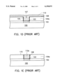
- FIGS. 1A to 1E are sectional views showing a conventional damascene process.
- a dielectric layer 102 is formed on a planarized substrate 100, wherein the dielectric layer includes a via plug 103, such as tungsten, electrically connected to a conducting region (not shown) on the substrate 100.
- a low-permissivity IMD layer 104 is formed on the dielectric layer 102 and via plug 103.
- a patterned photoresist layer 106 is formed on the IMD layer 104, wherein the pattern of the photoresist layer 106 exposes the area on the IMD layer 104 reserved for forming trenches.
- an etching process such as a reactive ion etching process (RIE) is performed on the IMD layer 104 by using photoresist layer 106 as a mask to from trenches 107 and expose the top of the via plug 103.
- RIE reactive ion etching process
- the photoresist layer 106 is stripped by a photoresist removal process, such as an oxygen plasma ashing process or a wet chemical removal process.
- a photoresist removal process such as an oxygen plasma ashing process or a wet chemical removal process.
- the photoresist removal process such as an oxygen plasma ashing process or a wet chemical removal process, damages the side walls 105 of the IMD layer 104a, and sometimes even causes a jagged profile on the side walls 105.
- the low-permissivity dielectric material of the sidewalls 105 tends to absorb moisture after a photoresist removal process, such as an oxygen plasma ashing process or a wet chemical removal process.
- the material filled into the trench 107 in the follow-up metallization process doesn't attach to the side walls 105 well and this causes degradation.
- a metal glue/barrier layer 108 conformal to the shape of the IMD layer 104a, is formed over the substrate 100 to increase the attachment between the metal layer formed in the follow-up process and other materials. Then, a metal layer 110 is deposited on the glue/barrier layer 108 and fills the trench 107.
- the undesired metal layer 110 on the metal glue/barrier layer 108 is removed by a chemical mechanical polishing process (CMP) to expose the top of the IMD layer 104a.
- CMP chemical mechanical polishing process
- the metal line 110a is electrically connected to the via plug 103.
- the liquid cleaner used in a follow-up post metal-CMP cleaning process sometimes reacts with the foregoing low-permissivity dielectric layer. Such a reaction increases the permissivity of the dielectric, and makes the surface 115 of the IMD layer 104a tend to absorb moisture, which further causes poor attachment between the IMD layer 104a and material formed on it.
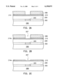
- a novel, degradation-free low-permissivity dielectrics patterning process for damascene starts with providing a substrate having a pre-formed dielectric layer with a via plug, and then forming an IMD layer, an insulating layer, and a hard mask layer in sequence.
- a photoresist layer is then formed on the hard mask layer and patterned to transfer a pattern onto the hard mask layer.
- the photoresist layer is removed by performing oxygen plasma ashing and a wet chemical treatment after an etching process is performed to expose the insulating layer.
- Another etching process is performed on the insulating layer and the IMD layer to expose the via plug by using the patterned hard mask layer as a mask, for forming trenches.
- a metal layer is next deposited into the trenches.
- the undesired metal on the hard mask layer and the hard mask layer are removed by a CMP process, wherein the metal line filled into the trench is electrically connected to the via plug. Finally, a post metal CMP cleaning is carried out.
- FIGS. 1A through 1E are cross-sectional views showing a conventional process for forming interconnects.
- FIGS. 2A through 2F are cross-sectional views showing the degradation-free low-permissivity dielectrics patterning process for damascene in a preferred embodiment according to the invention.
- the invention provides a degradation-free, low-permissivity dielectrics patterning process for damascene.
- a substrate 200 having a planarized surface already has a dielectric layer 202 on it, wherein the dielectric layer 202 contains a via plug 203, such as a tungsten plug, electrically connected to a conducting region (not shown) of the substrate 200.
- a low-permissivity IMD layer 204 with a thickness of about 5000-7000 ⁇ is formed to cover the dielectric layer 202 and the via plug 203.
- the IMD layer 204 preferably includes inorganic materials, such as HSQ and FSG, and organic materials, such as flare, SILK, and parylene.
- An insulating layer 212 such as a silicon oxide layer with a thickness of about 2000 ⁇ formed by CVD, is formed on the IMD layer 204.
- the insulating layer 212 is not only easier for the follow-up CMP than the IMD layer 204, but it can also protect the IMD layer 204 from being damaged by the CMP.
- a hard mask layer 214 such as titanium, titanium nitride, tantalum, tantalum nitride, or tungsten nitride formed by chemical vapor deposition (CVD) or physical vapor deposition (PVD), is formed over the top of the IMD layer 204, wherein the thickness of the hard mask layer is about 300-500 ⁇ .
- CVD chemical vapor deposition
- PVD physical vapor deposition
- a photoresist layer 206 is formed on the and mask layer 214 and partially exposes hard mask layer 214.
- an etching process such as a reactive ion etching (RIE) is performed on the hard mask layer 214 by using the photoresist layer 206 as a mask to form shallow trenches 207 on the hard mask layer 214a, and expose the insulating layer 212.
- the width of the shallow trench 207 is about the width of the trench for the metal line formed in a follow-up process.
- the photoresist layer 206 is stripped by a removal process, such as oxygen plasma ashing or wet chemical cleaning. Because of the protection from the insulating layer 212, the removal process, such as oxygen plasma ashing or wet chemical cleaning, used to remove the photoresist layer doesn't cause any damage, which otherwise might lead to degradation, on the IMD layer.
- a removal process such as oxygen plasma ashing or wet chemical cleaning
- an etching process such as RIE, is performed on the insulating layer 212 and the IMD layer 204 to form shallow trench 207a through the hard mask layer 214a, the insulating layer 212a, and the IMD layer 204a, and to expose the via plug 203.
- the shallow trench 207a is used to form a metal line in the follow-up damascene process.
- a glue/barrier layer 208 including titanium, titanium nitride, tantalum, tantalum nitride, or tungsten nitride formed by CVD or PVD, conformal to the surfaces of the hard mask layer 214a and the trench 207a, is used to improve the attachment of a metal layer formed by a follow-up process and other materials. Then, a metal layer 210, such as copper, aluminum, or aluminum-copper alloy, is formed on the glue/barrier layer 208, and filled into the shallow trench 207a.
- CMP is performed to remove the undesired metal layer 210 from the top of the glue/barrier layer 208 in order to expose the surface of the insulating layer 212a and form the metal line 210a.
- the thickness of the remaining insulating layer 212a is about 500-1000 ⁇ .
- the metal line 210a is electrically connected to the via plug 203.
- the low-permissivity IMD layer 204a is protected from being damaged by the liquid cleaner used in a post-CMP cleaning, and degradation is prevented.
- the IMD layer according to the invention is covered by an insulating layer and a hard mask layer, the damages on the IMD layer caused by the photoresist removal process and post-CMP cleaning process can be avoided.
- the process according to the invention is compatible with existing semiconductor fabrication process, so it is convenient for industry to employ the process according to the invention.
Abstract
A degradation-free, low-permittivity dielectrics patterning process for damascene starts with provision of a substrate, wherein the substrate has a dielectric layer and a via plug formed on it. Then, a inter-metal dielectric layer and an insulating layer are formed in sequence on the dielectric layer. A hard mask layer is next formed on the insulating layer, and is subsequently patterned. An etching process is performed on the insulating layer and the inter metal dielectric layer by using the patterned hard mask layer as a mask to form a metal line trench and expose the via plug. The metal line trench is then filled with metal by forming a metal layer on the hard mask layer. A metal line in the shallow trench is formed by performing chemical mechanical polishing on the metal layer to expose the insulating layer, and then performing post-chemical mechanical polishing cleaning.
Description
This application claims the priority benefit of Taiwan application serial no. 87107991, filed May 22, 1998.
1. Field of the Invention
This invention relates to a process for fabricating interconnects, and more particularly, to a degradation-free, low-permissivity dielectrics patterning process for damascene. Conventional patterning process gives rise to degradation of the low-permissivity dielectric layer; the process of this invention lessens this degradation.
2. Description of Related Art
Conventionally, there are two methods for fabricating interconnects, wherein one method includes forming a metal layer electrically connected to a via, patterning the photoresist layer on the metal layer, performing an etching process on the metal layer, and depositing an inter-metal dielectric (IMD) layer to cover the patterned metal layer. The other conventional method includes a damascene process of forming a dielectric layer, patterning the dielectric layer, forming trenches by an etching process, and filling the trenches with metal.
In a damascene process, using low-permissivity dielectric as IMD can reduce the occurrence of parasitic capacitance between interconnects and the IMD layer, and it can further decrease the RC delay. The low-permissivity dielectric includes inorganic materials, such as HSQ and FSG, and organic materials, such as flare, SILK, and parylene.
FIGS. 1A to 1E are sectional views showing a conventional damascene process.
Referring to FIG. 1A, a dielectric layer 102 is formed on a planarized substrate 100, wherein the dielectric layer includes a via plug 103, such as tungsten, electrically connected to a conducting region (not shown) on the substrate 100. A low-permissivity IMD layer 104 is formed on the dielectric layer 102 and via plug 103. Then, a patterned photoresist layer 106 is formed on the IMD layer 104, wherein the pattern of the photoresist layer 106 exposes the area on the IMD layer 104 reserved for forming trenches.
Referring to FIG. 1B, an etching process, such as a reactive ion etching process (RIE), is performed on the IMD layer 104 by using photoresist layer 106 as a mask to from trenches 107 and expose the top of the via plug 103.
Referring to FIG. 1C, the photoresist layer 106 is stripped by a photoresist removal process, such as an oxygen plasma ashing process or a wet chemical removal process.
However, the photoresist removal process, such as an oxygen plasma ashing process or a wet chemical removal process, damages the side walls 105 of the IMD layer 104a, and sometimes even causes a jagged profile on the side walls 105. Furthermore, the low-permissivity dielectric material of the sidewalls 105 tends to absorb moisture after a photoresist removal process, such as an oxygen plasma ashing process or a wet chemical removal process. As a result, the material filled into the trench 107 in the follow-up metallization process doesn't attach to the side walls 105 well and this causes degradation.
Referring to FIG. 1D, a metal glue/barrier layer 108, conformal to the shape of the IMD layer 104a, is formed over the substrate 100 to increase the attachment between the metal layer formed in the follow-up process and other materials. Then, a metal layer 110 is deposited on the glue/barrier layer 108 and fills the trench 107.
Referring to FIG. 1E, the undesired metal layer 110 on the metal glue/barrier layer 108 is removed by a chemical mechanical polishing process (CMP) to expose the top of the IMD layer 104a. This forms a metal line 110a and a patterned metal layer. The metal line 110a is electrically connected to the via plug 103.
However, the liquid cleaner used in a follow-up post metal-CMP cleaning process sometimes reacts with the foregoing low-permissivity dielectric layer. Such a reaction increases the permissivity of the dielectric, and makes the surface 115 of the IMD layer 104a tend to absorb moisture, which further causes poor attachment between the IMD layer 104a and material formed on it.
It is therefore an objective of the present invention to provide a degradation-free, low-permissivity dielectric patterning process for damascene, in order to prevent a low-permissivity dielectric layer from being degraded by a wet chemical treatment for post metal CMP cleaning.
In accordance with the foregoing and other objectives of the present invention, a novel, degradation-free low-permissivity dielectrics patterning process for damascene starts with providing a substrate having a pre-formed dielectric layer with a via plug, and then forming an IMD layer, an insulating layer, and a hard mask layer in sequence. A photoresist layer is then formed on the hard mask layer and patterned to transfer a pattern onto the hard mask layer. The photoresist layer is removed by performing oxygen plasma ashing and a wet chemical treatment after an etching process is performed to expose the insulating layer. Another etching process is performed on the insulating layer and the IMD layer to expose the via plug by using the patterned hard mask layer as a mask, for forming trenches. A metal layer is next deposited into the trenches. The undesired metal on the hard mask layer and the hard mask layer are removed by a CMP process, wherein the metal line filled into the trench is electrically connected to the via plug. Finally, a post metal CMP cleaning is carried out.
The invention can be more fully understood by reading the following detailed description of the preferred embodiments, with reference made to the accompanying drawings, wherein:
FIGS. 1A through 1E are cross-sectional views showing a conventional process for forming interconnects; and
FIGS. 2A through 2F are cross-sectional views showing the degradation-free low-permissivity dielectrics patterning process for damascene in a preferred embodiment according to the invention.
The invention provides a degradation-free, low-permissivity dielectrics patterning process for damascene. Referring to FIG. 2A, a substrate 200 having a planarized surface (the contained devices are not shown in the figure), already has a dielectric layer 202 on it, wherein the dielectric layer 202 contains a via plug 203, such as a tungsten plug, electrically connected to a conducting region (not shown) of the substrate 200. A low-permissivity IMD layer 204 with a thickness of about 5000-7000 Å is formed to cover the dielectric layer 202 and the via plug 203. The IMD layer 204 preferably includes inorganic materials, such as HSQ and FSG, and organic materials, such as flare, SILK, and parylene.
An insulating layer 212, such as a silicon oxide layer with a thickness of about 2000 Å formed by CVD, is formed on the IMD layer 204. The insulating layer 212 is not only easier for the follow-up CMP than the IMD layer 204, but it can also protect the IMD layer 204 from being damaged by the CMP.
A hard mask layer 214, such as titanium, titanium nitride, tantalum, tantalum nitride, or tungsten nitride formed by chemical vapor deposition (CVD) or physical vapor deposition (PVD), is formed over the top of the IMD layer 204, wherein the thickness of the hard mask layer is about 300-500 Å.
A photoresist layer 206 is formed on the and mask layer 214 and partially exposes hard mask layer 214.
Referring to FIG. 2B, an etching process, such as a reactive ion etching (RIE), is performed on the hard mask layer 214 by using the photoresist layer 206 as a mask to form shallow trenches 207 on the hard mask layer 214a, and expose the insulating layer 212. The width of the shallow trench 207 is about the width of the trench for the metal line formed in a follow-up process.
Referring to FIG. 2C, the photoresist layer 206 is stripped by a removal process, such as oxygen plasma ashing or wet chemical cleaning. Because of the protection from the insulating layer 212, the removal process, such as oxygen plasma ashing or wet chemical cleaning, used to remove the photoresist layer doesn't cause any damage, which otherwise might lead to degradation, on the IMD layer.
Referring to FIG. 2D, an etching process, such as RIE, is performed on the insulating layer 212 and the IMD layer 204 to form shallow trench 207a through the hard mask layer 214a, the insulating layer 212a, and the IMD layer 204a, and to expose the via plug 203. The shallow trench 207a is used to form a metal line in the follow-up damascene process.
Referring to FIG. 2E, a glue/barrier layer 208, including titanium, titanium nitride, tantalum, tantalum nitride, or tungsten nitride formed by CVD or PVD, conformal to the surfaces of the hard mask layer 214a and the trench 207a, is used to improve the attachment of a metal layer formed by a follow-up process and other materials. Then, a metal layer 210, such as copper, aluminum, or aluminum-copper alloy, is formed on the glue/barrier layer 208, and filled into the shallow trench 207a.
Referring to FIG. 2F, CMP is performed to remove the undesired metal layer 210 from the top of the glue/barrier layer 208 in order to expose the surface of the insulating layer 212a and form the metal line 210a. The thickness of the remaining insulating layer 212a is about 500-1000 Å. The metal line 210a is electrically connected to the via plug 203.
Because the IMD layer 204a is still covered by the insulating layer 212a, the low-permissivity IMD layer 204a is protected from being damaged by the liquid cleaner used in a post-CMP cleaning, and degradation is prevented.
In accordance with the foregoing the specifics of the invention include:
1. Because the IMD layer according to the invention is covered by an insulating layer and a hard mask layer, the damages on the IMD layer caused by the photoresist removal process and post-CMP cleaning process can be avoided.
2. The process according to the invention is compatible with existing semiconductor fabrication process, so it is convenient for industry to employ the process according to the invention.
The invention has been described using exemplary preferred embodiments. However, it is to be understood that the scope of the invention is not limited to the disclosed embodiments. On the contrary it is intended to cover various modifications and similar arrangements. The scope of the claims, therefore, should be accorded the broadest interpretation so as to encompass all such modifications and similar arrangements.
Claims (36)
1. A degradation-free, low-permissivity dielectric patterning process for damascene, the process comprising:
providing a substrate, wherein the substrate has a dielectric layer and a via plug formed on it;
forming an inter-metal dielectric layer on the dielectric layer, wherein the inter-metal dielectric layer has a thickness;
forming an insulating layer on the inter-metal dielectric layer for protecting the inter-metal dielectric layer from being damaged by a photoresist removal process and a post-chemical mechanical polishing cleaning process, wherein the insulating layer has a thickness and the insulating layer is thinner than the inter-metal dielectric layer;
forming a hard mask layer on the insulating layer, wherein the hard mask layer has a thickness;
forming and patterning a photoresist layer on the hard mask layer to expose a portion of the hard mask layer;
performing an etching process on the hard mask layer until the insulating layer is exposed to form a shallow trench;
performing oxygen plasma ashing and wet chemical cleaning to remove the photoresist layer;
performing an etching process on the insulating layer and the inter-metal dielectric layer by using the hard mask layer as a mask to form a metal line trench and expose the via plug;
forming a glue/barrier layer conformal to the metal line trench and the hard mask layer;
forming a metal layer on the glue/barrier layer to fill the metal line trench;
performing chemical mechanical polishing on the metal layer to expose the insulating layer and form a metal line in the shallow trench, wherein the metal line is electrically connected to the via plug; and
performing post-chemical mechanical polishing cleaning.
2. The process of claim 1, wherein the inter-metal dielectric layer includes HSQ, FSG, flare, SILK or parylene.
3. The process of claim 1, wherein the thickness of the inter-metal dielectric layer is about 5000-7000 Å.
4. The process of claim 1, wherein the insulating layer includes silicon oxide.
5. The process of claim 1, wherein the thickness of the insulating layer is about 2000 Å.
6. The process of claim 1, wherein the hard mask layer includes titanium, titanium nitride, tantalum, tantalum nitride, or tungsten nitride.
7. The process of claim 1, wherein the thickness of the hard mask layer is about 300-500 Å.
8. The process of claim 1, wherein the etching process performed on the hard mask layer includes reactive ion etching.
9. The process of claim 1, wherein the etching process performed on the insulating layer and the inter-metal dielectric layer includes reactive ion etching.
10. The process of claim 1, wherein the glue/barrier layer includes titanium, titanium nitride, tantalum, tantalum nitride, or tungsten nitride.
11. A degradation-free, low-permissivity dielectrics patterning process for damascene on a substrate, wherein the substrate has a dielectric layer and a via plug formed thereon, the process comprising:
forming an inter-metal dielectric layer on the dielectric layer, wherein the inter-metal dielectric layer has a thickness;
forming an insulating layer on the inter-metal dielectric layer, wherein the insulating layer has a thickness, and the insulating layer is thinner than the inter-metal dielectric layer;
forming a hard mask layer on the insulating layer, wherein the hard mask layer has a thickness;
patterning the hard mask layer to form a shallow trench and expose the insulating layer;
performing an etching process on the insulating layer and the inter-metal dielectric layer by using the hard mask layer as a mask to form a metal line trench and expose the via plug;
forming a metal layer on the hard mask layer to fill the metal line trench; and
performing chemical mechanical polishing on the metal layer to expose the insulating layer and form a metal line in the shallow trench, wherein the metal line is electrically connected to the via plug.
12. The process of claim 11, wherein the inter-metal dielectric layer includes HSQ, FSG, flare, SILK or parylene.
13. The process of claim 11, wherein the thickness of the inter-metal dielectric layer is about 5000-7000 Å.
14. The process of claim 11, wherein the insulating layer includes silicon oxide.
15. The process of claim 11, wherein the thickness of the insulating layer is about 2000 Å.
16. The process of claim 11, wherein the hard mask layer includes titanium, titanium nitride, tantalum, tantalum nitride, or tungsten nitride.
17. The process of claim 11, wherein the thickness of the hard mask layer is about 300-500 Å.
18. The process of claim 11, wherein the steps of patterning the hard mask layer comprise:
forming a photoresist layer on the hard mask layer, wherein the photoresist layer exposes a portion of the hard mask layer;
performing an etching process to form the shallow trench and expose the insulating layer; and
removing the photoresist layer by oxygen plasma ashing and wet chemical cleaning.
19. The process of claim 18, wherein the etching process performed on the hard mask layer includes reactive ion etching.
20. The process of claim 11, wherein the etching process performed on the insulating layer and the inter-metal dielectric layer includes reactive ion etching.
21. The process of claim 11, wherein the steps of forming the metal layer further comprises forming a glue/barrier layer conformal to the hard mask layer and the metal line trench.
22. The process of claim 21, wherein the glue/barrier layer includes titanium, titanium nitride, tantalum, tantalum nitride, or tungsten nitride.
23. The process of claim 11, further comprising a post-chemical mechanical polishing cleaning after the step of performing the chemical-mechanical polishing.
24. A degradation-free, low-permissivity dielectrics patterning process for damascene on a substrate, wherein the substrate has a dielectric layer and a via plug formed thereon, the process comprising:
forming an inter-metal dielectric layer on the dielectric layer, wherein the inter-metal dielectric layer has a thickness;
forming an insulating layer on the inter-metal dielectric layer, wherein the insulating layer has a thickness and the insulating layer is thinner than the inter-metal dielectric layer;
forming a hard mask layer on the insulating layer, wherein the hard mask layer has a thickness;
patterning the hard mask layer to form a shallow trench and expose a portion of the inter-metal dielectric layer;
performing an etching process on the insulating layer and the inter-metal dielectric layer by using the hard mask layer as a mask to form a metal line trench and expose the via plug;
forming a metal layer on the hard mask layer to fill the metal line trench; and
performing an etching process on the metal layer to expose the insulating layer and form a metal line in the shallow trench, wherein the metal line is electrically connected to the via plug.
25. The process of claim 24, wherein inter-metal dielectric layer includes HSQ, FSG, flare, SILK or parylene.
26. The process of claim 24, wherein the thickness of the inner-metal dielectric layer is about 5000-7000 Å.
27. The process of claim 24, wherein the insulating layer includes silicon oxide.
28. The process of claim 24, wherein the thickness of the insulating layer is about 2000 Å.
29. The process of claim 24, wherein the hard mask layer includes titanium, titanium nitride, tantalum, tantalum nitride, or tungsten nitride.
30. The process of claim 24, wherein the thickness of the hard mask layer is about 300-500 Å.
31. The process of claim 24, wherein the steps of patterning the hard mask layer comprise:
forming a photoresist layer on the hard mask layer, wherein the photoresist layer exposes a portion of the hard mask layer;
performing an etching process to form the shallow trench and expose the insulating layer; and
removing the photoresist layer by oxygen plasma ashing and wet chemical cleaning.
32. The process of claim 31, wherein the etching process performed on the hard mask layer includes reactive ion etching.
33. The process of claim 24, wherein the etching process performed on the inter-metal dielectric layer includes reactive ion etching.
34. The process of claim 24, wherein the steps of forming the metal layer further comprise forming a glue/barrier layer conformal to the hard mask layer and the metal line trench, wherein the glue/barrier layer further has contact with the dielectric layer.
35. The process of claim 34, wherein the glue/barrier layer includes titanium, titanium nitride, tantalum, tantalum nitride, or tungsten nitride.
36. The process of claim 24, wherein the etching process performed on the metal layer above the hard mask layer comprises performing chemical mechanical polishing and post-chemical mechanical polishing cleaning.
Priority Applications (1)
| Application Number | Priority Date | Filing Date | Title |
|---|---|---|---|
| US10/251,451 US20030022110A1 (en) | 1998-05-22 | 2002-09-20 | Degradation-free low-permittivity dielectrics patterning process for damascene |
Applications Claiming Priority (2)
| Application Number | Priority Date | Filing Date | Title |
|---|---|---|---|
| TW87107991 | 1998-05-22 | ||
| TW087107991A TW389988B (en) | 1998-05-22 | 1998-05-22 | Method for forming metal interconnect in dielectric layer with low dielectric constant |
Related Child Applications (1)
| Application Number | Title | Priority Date | Filing Date |
|---|---|---|---|
| US62874300A Continuation | 1998-05-22 | 2000-07-31 |
Publications (1)
| Publication Number | Publication Date |
|---|---|
| US6150073A true US6150073A (en) | 2000-11-21 |
Family
ID=21630163
Family Applications (2)
| Application Number | Title | Priority Date | Filing Date |
|---|---|---|---|
| US09/111,505 Expired - Lifetime US6150073A (en) | 1998-05-22 | 1998-07-07 | Degradation-free low-permittivity dielectrics patterning process for damascene |
| US10/251,451 Abandoned US20030022110A1 (en) | 1998-05-22 | 2002-09-20 | Degradation-free low-permittivity dielectrics patterning process for damascene |
Family Applications After (1)
| Application Number | Title | Priority Date | Filing Date |
|---|---|---|---|
| US10/251,451 Abandoned US20030022110A1 (en) | 1998-05-22 | 2002-09-20 | Degradation-free low-permittivity dielectrics patterning process for damascene |
Country Status (2)
| Country | Link |
|---|---|
| US (2) | US6150073A (en) |
| TW (1) | TW389988B (en) |
Cited By (19)
| Publication number | Priority date | Publication date | Assignee | Title |
|---|---|---|---|---|
| WO2002069378A1 (en) * | 2001-02-27 | 2002-09-06 | Infineon Technologies Ag | Method for removing a mask layer from a semiconductor substrate |
| DE10134100A1 (en) * | 2001-07-13 | 2002-10-02 | Infineon Technologies Ag | Production of integrated semiconductor circuit comprises forming first electrically insulating layer on semiconductor substrate, applying and structuring mask layer, etching trenches in insulating layer, and further processing |
| EP1276146A2 (en) * | 2001-07-09 | 2003-01-15 | Texas Instruments Incorporated | Damascene cap layer process for integrated circuit interconnects |
| EP1276147A2 (en) * | 2001-07-09 | 2003-01-15 | Texas Instruments Incorporated | Dual hardmask process for the formation of copper/low-K interconnects |
| GB2380316A (en) * | 2001-09-28 | 2003-04-02 | Agere Systems Inc | Mask layer and interconnect structure for dual damascene semiconductor manufacturing |
| US6551930B1 (en) * | 2000-06-07 | 2003-04-22 | Stmicroelectronics S.A. | Etching an organic material layer, particularly for producing interconnections of the damascene type |
| US6635409B1 (en) * | 2001-07-12 | 2003-10-21 | Advanced Micro Devices, Inc. | Method of strengthening photoresist to prevent pattern collapse |
| US6638878B2 (en) | 2001-10-02 | 2003-10-28 | International Business Machines Corporation | Film planarization for low-k polymers used in semiconductor structures |
| US20030230550A1 (en) * | 2002-06-12 | 2003-12-18 | Kuang-Yeh Chang | Lithography process |
| US20040124528A1 (en) * | 2002-12-30 | 2004-07-01 | Lee Jae Suk | Metal line structures in semiconductor devices and methods of forming the same |
| US20040148918A1 (en) * | 2002-11-04 | 2004-08-05 | Electrolux Outdoor Products Limited A Corporation Of United Kingdom | Trimmer |
| US20040161922A1 (en) * | 2000-09-13 | 2004-08-19 | Shipley Company, L.L.C. | Electronic device manufacture |
| US20040251234A1 (en) * | 2003-06-13 | 2004-12-16 | Kaushik Kumar | Bilayered metal hardmasks for use in dual damascene etch schemes |
| US20040266106A1 (en) * | 2003-06-30 | 2004-12-30 | Hynix Semiconductor Inc. | Method for forming bit line of flash device |
| US20050032358A1 (en) * | 2000-02-23 | 2005-02-10 | Matsushita Electric Industrial Co., Ltd. | Semiconductor device and method for fabricating the same |
| US6864180B2 (en) | 2001-10-02 | 2005-03-08 | International Business Machines Corporation | Method for reworking low-k polymers used in semiconductor structures |
| US20060141766A1 (en) * | 2004-12-29 | 2006-06-29 | Hynix Semiconductor Inc. | Method of manufacturing semiconductor device |
| US20070128553A1 (en) * | 2005-10-19 | 2007-06-07 | Joerg Linz | Method for forming feature definitions |
| US20100190272A1 (en) * | 2009-01-23 | 2010-07-29 | United Microelectronics Corp. | Rework method of metal hard mask |
Families Citing this family (4)
| Publication number | Priority date | Publication date | Assignee | Title |
|---|---|---|---|---|
| US7748621B2 (en) * | 2005-06-06 | 2010-07-06 | International Business Machines Corporation | Method and system for dissemination of paperless transaction receipts in non-networked environments |
| JP4600836B2 (en) * | 2006-08-09 | 2010-12-22 | エルピーダメモリ株式会社 | Manufacturing method of semiconductor memory device |
| US8921150B2 (en) | 2012-12-06 | 2014-12-30 | Taiwan Semiconductor Manufacturing Co., Ltd. | Process to achieve contact protrusion for single damascene via |
| ITTO20130035A1 (en) * | 2013-01-15 | 2014-07-16 | Inst Rundfunktechnik Gmbh | SENDEEINRICHTUNG ZUM DRAHTLOSEN UEBERTRAGEN EINES MPEG2-TS KOMPATIBLEN DATENSTROMS |
Citations (3)
| Publication number | Priority date | Publication date | Assignee | Title |
|---|---|---|---|---|
| US5565384A (en) * | 1994-04-28 | 1996-10-15 | Texas Instruments Inc | Self-aligned via using low permittivity dielectric |
| US5759906A (en) * | 1997-04-11 | 1998-06-02 | Industrial Technology Research Institute | Planarization method for intermetal dielectrics between multilevel interconnections on integrated circuits |
| US5930639A (en) * | 1996-04-08 | 1999-07-27 | Micron Technology, Inc. | Method for precision etching of platinum electrodes |
Family Cites Families (5)
| Publication number | Priority date | Publication date | Assignee | Title |
|---|---|---|---|---|
| GB9215653D0 (en) * | 1992-07-23 | 1992-09-09 | Philips Electronics Uk Ltd | A method of manufacturing a semiconductor device comprising an insulated gate field effect device |
| US5891799A (en) * | 1997-08-18 | 1999-04-06 | Industrial Technology Research Institute | Method for making stacked and borderless via structures for multilevel metal interconnections on semiconductor substrates |
| TW359008B (en) * | 1997-12-20 | 1999-05-21 | United Microelectronics Corp | Double metal embedding |
| TW392324B (en) * | 1998-01-23 | 2000-06-01 | United Microelectronics Corp | Dual damascene process |
| US6054384A (en) * | 1998-05-19 | 2000-04-25 | Advanced Micro Devices, Inc. | Use of hard masks during etching of openings in integrated circuits for high etch selectivity |
-
1998
- 1998-05-22 TW TW087107991A patent/TW389988B/en not_active IP Right Cessation
- 1998-07-07 US US09/111,505 patent/US6150073A/en not_active Expired - Lifetime
-
2002
- 2002-09-20 US US10/251,451 patent/US20030022110A1/en not_active Abandoned
Patent Citations (3)
| Publication number | Priority date | Publication date | Assignee | Title |
|---|---|---|---|---|
| US5565384A (en) * | 1994-04-28 | 1996-10-15 | Texas Instruments Inc | Self-aligned via using low permittivity dielectric |
| US5930639A (en) * | 1996-04-08 | 1999-07-27 | Micron Technology, Inc. | Method for precision etching of platinum electrodes |
| US5759906A (en) * | 1997-04-11 | 1998-06-02 | Industrial Technology Research Institute | Planarization method for intermetal dielectrics between multilevel interconnections on integrated circuits |
Cited By (32)
| Publication number | Priority date | Publication date | Assignee | Title |
|---|---|---|---|---|
| US20060128141A1 (en) * | 2000-02-23 | 2006-06-15 | Matsushita Electric Industrial Co., Ltd. | Semiconductor device and method for fabricating the same |
| US20050032358A1 (en) * | 2000-02-23 | 2005-02-10 | Matsushita Electric Industrial Co., Ltd. | Semiconductor device and method for fabricating the same |
| US7030009B2 (en) * | 2000-02-23 | 2006-04-18 | Matsushita Electric Industrial Co., Ltd. | Method for forming metal interconnect in a carbon containing silicon oxide film |
| US6551930B1 (en) * | 2000-06-07 | 2003-04-22 | Stmicroelectronics S.A. | Etching an organic material layer, particularly for producing interconnections of the damascene type |
| US7294453B2 (en) * | 2000-09-13 | 2007-11-13 | Shipley Company, L.L.C. | Electronic device manufacture |
| US20040161922A1 (en) * | 2000-09-13 | 2004-08-19 | Shipley Company, L.L.C. | Electronic device manufacture |
| US7129173B2 (en) | 2001-02-27 | 2006-10-31 | Infineon Technologies Ag | Process for producing and removing a mask layer |
| US20040048479A1 (en) * | 2001-02-27 | 2004-03-11 | Heike Drummer | Process for producing and removing a mask layer |
| WO2002069378A1 (en) * | 2001-02-27 | 2002-09-06 | Infineon Technologies Ag | Method for removing a mask layer from a semiconductor substrate |
| EP1276147A2 (en) * | 2001-07-09 | 2003-01-15 | Texas Instruments Incorporated | Dual hardmask process for the formation of copper/low-K interconnects |
| EP1276147A3 (en) * | 2001-07-09 | 2003-07-02 | Texas Instruments Incorporated | Dual hardmask process for the formation of copper/low-K interconnects |
| EP1276146A3 (en) * | 2001-07-09 | 2003-06-11 | Texas Instruments Incorporated | Damascene cap layer process for integrated circuit interconnects |
| EP1276146A2 (en) * | 2001-07-09 | 2003-01-15 | Texas Instruments Incorporated | Damascene cap layer process for integrated circuit interconnects |
| US6635409B1 (en) * | 2001-07-12 | 2003-10-21 | Advanced Micro Devices, Inc. | Method of strengthening photoresist to prevent pattern collapse |
| DE10134100A1 (en) * | 2001-07-13 | 2002-10-02 | Infineon Technologies Ag | Production of integrated semiconductor circuit comprises forming first electrically insulating layer on semiconductor substrate, applying and structuring mask layer, etching trenches in insulating layer, and further processing |
| GB2380316B (en) * | 2001-09-28 | 2005-08-24 | Agere Systems Inc | Mask layer and interconnect structure for dual damascene semiconductor manufacturing |
| GB2380316A (en) * | 2001-09-28 | 2003-04-02 | Agere Systems Inc | Mask layer and interconnect structure for dual damascene semiconductor manufacturing |
| US6864180B2 (en) | 2001-10-02 | 2005-03-08 | International Business Machines Corporation | Method for reworking low-k polymers used in semiconductor structures |
| US6638878B2 (en) | 2001-10-02 | 2003-10-28 | International Business Machines Corporation | Film planarization for low-k polymers used in semiconductor structures |
| US20030230550A1 (en) * | 2002-06-12 | 2003-12-18 | Kuang-Yeh Chang | Lithography process |
| US20040148918A1 (en) * | 2002-11-04 | 2004-08-05 | Electrolux Outdoor Products Limited A Corporation Of United Kingdom | Trimmer |
| US7584542B2 (en) | 2002-11-04 | 2009-09-08 | Husqvarna Uk Limited | Trimmer |
| US20040124528A1 (en) * | 2002-12-30 | 2004-07-01 | Lee Jae Suk | Metal line structures in semiconductor devices and methods of forming the same |
| US7052621B2 (en) * | 2003-06-13 | 2006-05-30 | Infineon Technologies Ag | Bilayered metal hardmasks for use in Dual Damascene etch schemes |
| US20060113278A1 (en) * | 2003-06-13 | 2006-06-01 | Kaushik Kumar | Bilayered metal hardmasks for use in dual damascene etch schemes |
| US7241681B2 (en) | 2003-06-13 | 2007-07-10 | Infineon Technologies Ag | Bilayered metal hardmasks for use in dual damascene etch schemes |
| US20040251234A1 (en) * | 2003-06-13 | 2004-12-16 | Kaushik Kumar | Bilayered metal hardmasks for use in dual damascene etch schemes |
| US6964921B2 (en) * | 2003-06-30 | 2005-11-15 | Hynix Semiconductor Inc. | Method for forming bit line of flash device |
| US20040266106A1 (en) * | 2003-06-30 | 2004-12-30 | Hynix Semiconductor Inc. | Method for forming bit line of flash device |
| US20060141766A1 (en) * | 2004-12-29 | 2006-06-29 | Hynix Semiconductor Inc. | Method of manufacturing semiconductor device |
| US20070128553A1 (en) * | 2005-10-19 | 2007-06-07 | Joerg Linz | Method for forming feature definitions |
| US20100190272A1 (en) * | 2009-01-23 | 2010-07-29 | United Microelectronics Corp. | Rework method of metal hard mask |
Also Published As
| Publication number | Publication date |
|---|---|
| US20030022110A1 (en) | 2003-01-30 |
| TW389988B (en) | 2000-05-11 |
Similar Documents
| Publication | Publication Date | Title |
|---|---|---|
| US6150073A (en) | Degradation-free low-permittivity dielectrics patterning process for damascene | |
| US6972259B2 (en) | Method for forming openings in low dielectric constant material layer | |
| US6309955B1 (en) | Method for using a CVD organic barc as a hard mask during via etch | |
| US6846741B2 (en) | Sacrificial metal spacer damascene process | |
| US6452251B1 (en) | Damascene metal capacitor | |
| US6787911B1 (en) | Interconnect with low dielectric constant insulators for semiconductor integrated circuit manufacturing | |
| US6150272A (en) | Method for making metal plug contacts and metal lines in an insulating layer by chemical/mechanical polishing that reduces polishing-induced damage | |
| US7037836B2 (en) | Method of manufacturing a semiconductor device without oxidized copper layer | |
| US6268283B1 (en) | Method for forming dual damascene structure | |
| US6074942A (en) | Method for forming a dual damascene contact and interconnect | |
| KR100366632B1 (en) | Semiconductor device for suppressing detachment of conducting layer and method thereof | |
| US20070032062A1 (en) | Methods of Forming Dual-Damascene Metal Wiring Patterns for Integrated Circuit Devices and Wiring Patterns Formed Thereby | |
| US20100219529A1 (en) | Method and apparatus for forming metal-metal oxide etch stop/barrier for integrated circuit interconnects | |
| US20020168849A1 (en) | Method of manufacturing interconnection line in semiconductor device | |
| US6255226B1 (en) | Optimized metal etch process to enable the use of aluminum plugs | |
| US6084304A (en) | Structure of metallization | |
| US20030001264A1 (en) | Apparatus for integrating low dielectric constant materials into a multilevel metallization and interconnect structure | |
| US7397124B2 (en) | Process of metal interconnects | |
| US6028363A (en) | Vertical via/contact | |
| US6191025B1 (en) | Method of fabricating a damascene structure for copper medullization | |
| US6475810B1 (en) | Method of manufacturing embedded organic stop layer for dual damascene patterning | |
| US5897374A (en) | Vertical via/contact with undercut dielectric | |
| US6645864B1 (en) | Physical vapor deposition of an amorphous silicon liner to eliminate resist poisoning | |
| US6228757B1 (en) | Process for forming metal interconnects with reduced or eliminated metal recess in vias | |
| US6403471B1 (en) | Method of forming a dual damascene structure including smoothing the top part of a via |
Legal Events
| Date | Code | Title | Description |
|---|---|---|---|
| AS | Assignment |
Owner name: UNITED MICROELECTRONICS CORP., TAIWAN Free format text: ASSIGNMENT OF ASSIGNORS INTEREST;ASSIGNOR:HUANG, YIMIN;REEL/FRAME:009307/0378 Effective date: 19980623 |
|
| STCF | Information on status: patent grant |
Free format text: PATENTED CASE |
|
| FEPP | Fee payment procedure |
Free format text: PAYOR NUMBER ASSIGNED (ORIGINAL EVENT CODE: ASPN); ENTITY STATUS OF PATENT OWNER: LARGE ENTITY |
|
| FPAY | Fee payment |
Year of fee payment: 4 |
|
| FPAY | Fee payment |
Year of fee payment: 8 |
|
| FPAY | Fee payment |
Year of fee payment: 12 |