US6150059A - Photomask and method of exposure using same - Google Patents
Photomask and method of exposure using same Download PDFInfo
- Publication number
- US6150059A US6150059A US09/181,566 US18156698A US6150059A US 6150059 A US6150059 A US 6150059A US 18156698 A US18156698 A US 18156698A US 6150059 A US6150059 A US 6150059A
- Authority
- US
- United States
- Prior art keywords
- holes
- photomask
- auxiliary
- main
- light beam
- Prior art date
- Legal status (The legal status is an assumption and is not a legal conclusion. Google has not performed a legal analysis and makes no representation as to the accuracy of the status listed.)
- Expired - Lifetime
Links
Images

Classifications
-
- G—PHYSICS
- G03—PHOTOGRAPHY; CINEMATOGRAPHY; ANALOGOUS TECHNIQUES USING WAVES OTHER THAN OPTICAL WAVES; ELECTROGRAPHY; HOLOGRAPHY
- G03F—PHOTOMECHANICAL PRODUCTION OF TEXTURED OR PATTERNED SURFACES, e.g. FOR PRINTING, FOR PROCESSING OF SEMICONDUCTOR DEVICES; MATERIALS THEREFOR; ORIGINALS THEREFOR; APPARATUS SPECIALLY ADAPTED THEREFOR
- G03F7/00—Photomechanical, e.g. photolithographic, production of textured or patterned surfaces, e.g. printing surfaces; Materials therefor, e.g. comprising photoresists; Apparatus specially adapted therefor
- G03F7/70—Microphotolithographic exposure; Apparatus therefor
- G03F7/70425—Imaging strategies, e.g. for increasing throughput or resolution, printing product fields larger than the image field or compensating lithography- or non-lithography errors, e.g. proximity correction, mix-and-match, stitching or double patterning
- G03F7/70433—Layout for increasing efficiency or for compensating imaging errors, e.g. layout of exposure fields for reducing focus errors; Use of mask features for increasing efficiency or for compensating imaging errors
-
- G—PHYSICS
- G03—PHOTOGRAPHY; CINEMATOGRAPHY; ANALOGOUS TECHNIQUES USING WAVES OTHER THAN OPTICAL WAVES; ELECTROGRAPHY; HOLOGRAPHY
- G03F—PHOTOMECHANICAL PRODUCTION OF TEXTURED OR PATTERNED SURFACES, e.g. FOR PRINTING, FOR PROCESSING OF SEMICONDUCTOR DEVICES; MATERIALS THEREFOR; ORIGINALS THEREFOR; APPARATUS SPECIALLY ADAPTED THEREFOR
- G03F1/00—Originals for photomechanical production of textured or patterned surfaces, e.g., masks, photo-masks, reticles; Mask blanks or pellicles therefor; Containers specially adapted therefor; Preparation thereof
- G03F1/36—Masks having proximity correction features; Preparation thereof, e.g. optical proximity correction [OPC] design processes
-
- G—PHYSICS
- G03—PHOTOGRAPHY; CINEMATOGRAPHY; ANALOGOUS TECHNIQUES USING WAVES OTHER THAN OPTICAL WAVES; ELECTROGRAPHY; HOLOGRAPHY
- G03F—PHOTOMECHANICAL PRODUCTION OF TEXTURED OR PATTERNED SURFACES, e.g. FOR PRINTING, FOR PROCESSING OF SEMICONDUCTOR DEVICES; MATERIALS THEREFOR; ORIGINALS THEREFOR; APPARATUS SPECIALLY ADAPTED THEREFOR
- G03F1/00—Originals for photomechanical production of textured or patterned surfaces, e.g., masks, photo-masks, reticles; Mask blanks or pellicles therefor; Containers specially adapted therefor; Preparation thereof
- G03F1/68—Preparation processes not covered by groups G03F1/20 - G03F1/50
- G03F1/70—Adapting basic layout or design of masks to lithographic process requirements, e.g., second iteration correction of mask patterns for imaging
Definitions
- the present invention relates to a photomask used in an apparatus for manufacturing a semiconductor integrated circuit and to a method which uses this photomask to expose the pattern of a semiconductor integrated circuit.
- the increasing level of integration of semiconductor integrated circuits has resulted in a rapid shrinking of circuit patterns used therein.
- the lithography technology that uses a projection-type exposure apparatus has a limit of resolution that is related to the wavelength of the light source.
- One known half-tone phase-shift mask for the purpose of improving the resolution for hole patterns is known by its disclosure in the Japanese Unexamined Patent Publication (KOKAI) No. 4-136854.
- a half-tone phase-shift mask With a half-tone phase-shift mask, a translucent phase-shift mask is used in place of the usual light-blocking film.
- This method makes use of a mask onto which are provided auxiliary holes 5, which are below the resolving limit of the projection lens, in the vicinity of the area surrounding the hole pattern 4.
- This mask imparts a phase shift effect to isolated holes, and improves the resolution when used with illumination having a small numerical aperture ⁇ of 0.3 or smaller in an illumination optical system.
- a mask with auxiliary holes or auxiliary shifters such as shown in FIG. 6 and FIG. 7 is effective with respect to isolated holes.
- the arrangement of holes in the contact hole pattern of a memory device has parts in which the holes are arranged in high concentration.
- the present invention has the following basic technical constitution.
- the first aspect of the present invention is a photomask for the purpose of forming a plurality of pattern parts on at least part of the pattern of a semiconductor device, this mask having a plurality of main holes at locations which are opposite the positions at which the above-noted plurality of pattern parts are to be formed, each one of these main holes passes a prescribed light beam that is irradiated thereonto, this photomask further having at the plurality of minute auxiliary holes between the main holes and each of which passes a light beam therethrough that is of a degree that does not transfer to a surface of a substrate at the time of exposure.
- the second aspect of the present invention is a photomask which has an optical phase shifter provided at at least one of the mutually adjacent main and auxiliary holes of the plurality of main and plurality of auxiliary holes.
- the third aspect of the present invention is a method of exposure which uses a photomask according to the first aspect of the present invention to perform exposure using deformed illumination in which the surrounding area of the illumination light source is bright.
- the fourth aspect of the present invention is a method of exposure which uses a photomask according to the second aspect of the present invention to perform exposure using illumination from a light source with an illumination optical system having a small numerical aperture.
- a photomask according to the present invention can be used, for example, as a photomask having the contact hole pattern for a memory device.
- matrix lines would be drawn between the above-noted contact hole patterns to connect those holes, thereby establishing the points of intersection of the matrix lines with minute auxiliary holes that are not transferred to a surface of a substrate when it is exposed being added at some or all of the matrix points at which there is no contact hole pattern.
- a photomask without the above-noted phase-shifting means it is desirable that the exposure be performed using deformed illumination, in which the peripheral area of the illumination is bright and, in the case in which a photomask having the above-noted phase shifters is used, a conventional light source is used, but with the light beam considerably contracted.
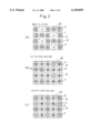
- FIG. 1(A) is a plan view which shows an example of the configuration of the pattern of a semiconductor circuit to be described using a photomask according to the present invention
- FIG. 1(B) is a plan view which shows the configuration of a specific example of a photomask that is used for the bit line contact holes according to the present invention.
- FIG. 1(C) is a plan view which shows a specific example of a photomask that is used for capacitive contact holes according to the present invention.
- FIG. 2(A) is a plan view which shows an example of the configuration of the pattern of a semiconductor circuit to be described using a photomask according to the present invention
- FIG. 2(B) is a plan view which shows another specific example of a photomask that is used for the bit line contact holes according to the present invention.
- FIG. 2(C) is a plan view which shows another specific example of a photomask that is used for capacitive contact holes according to the present invention.
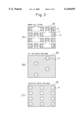
- FIG. 3A is a plan view which shows an example of the configuration of a pattern of a semiconductor circuit to be described using a photomask according to the prior art
- FIG. 3(B) is a plan view which shows the configuration of a specific example of a photomask that is used for bit line contact holes according to the prior art.
- FIG. 3(C) is a plan view which shows the configuration of a specific example of a photomask that is used for capacitive contact holes according to the prior art.
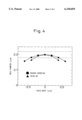
- FIG. 4 is a graph which shows the difference between the focal depth of field of a prior art photomask and a photomask according to the present invention.
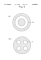
- FIG. 5(A) and FIG. 5(B) are plan views which show the shapes of deformed illumination according to the present invention.
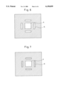
- FIG. 6 is a plan view which shows an example of a photomask for isolated holes, in which the auxiliary holes of the past are used.
- FIG. 7 is a plan view which shows an example of a photomask for isolated holes, in which the auxiliary shifters of the past are used.
- FIG. 1(B) and FIG. 1(C) are plan views which show examples of photomasks 20 and 22 according to the present invention, in which in order to form a plurality of pattern parts of at least part of the semiconductor element pattern 25 shown in FIG. 1(A), for example, the bit line contact holes 2 or capacitive contact holes 3, at locations which are in opposition to locations at which parts 2 or 3 are to be formed, a plurality of main holes 4 which cause the passage of a prescribed light beam irradiated to each one of portions on which the patterns 2 or 3 of a plurality of the pattern, is formed, respectively, are provided.
- the semiconductor device which uses the photomasks 20 and 22 according to the present invention be a memory device, and at least part of the pattern of this semiconductor device can be either contact holes 2 or capacitive contact holes 3, the present invention presenting no restriction in this regard.
- main hole 4 and auxiliary hole 5 in the present invention be arranged so as to form a periodic hole group within the photomasks 20 and 22.
- auxiliary holes 5 provided in the photomasks 20 and 22 in the present invention are provided at prescribed positions with respect to each of the groups of main holes 4, this not necessarily being restricted to the center part thereof, it is desirable that they be provided at either the intersection points 7 of virtual matrix lines 6 that run between prescribed positions in two directions, or at intersection points 7 of virtual lines 6' that would be formed by dividing the above-noted virtual matrix lines 6 into equal divisions.
- the pattern structure that is shown in FIG. 1(A), which is the pattern 25 of a semiconductor device that is to be used in photomasks 20 and 22 of the present invention, has the same pattern configuration as the pattern structure shown as the prior art in FIG. 3(A) and, in the same manner, the structure of the photomask 20 for the bit line contact holes, which is shown in FIG. 1(B) corresponds to the photomask 30 for the bit line contact holes in the prior art as shown in FIG. 3(B), and the structure of the photomask 22 for the capacitive contact holes shown according to the present invention as shown in FIG. 1(C) corresponds to that of the photomask 32 for bit line contact holes in the prior art, as shown in FIG. 3(C).
- the photomask 20 according to the present invention consists of the photomask 30 of the prior art, as shown in FIG. 3(B), with the addition of the auxiliary holes 5, the action of which is to intentionally cause a diffraction of the light beam used for exposure, thereby increasing the focal depth of field.
- an activated region 1 having a convex memory cell pattern as shown in FIG. 1(A) (the same pattern is formed as shown in FIG. 3(A)) that is formed periodically and in a concentrated pattern.
- bit line contact holes 2 and capacitive contact holes 3 are disposed so as to be positioned at the points of intersection 7 of the matrix lines 6 that connect the contact holes.
- the auxiliary holes 5 that are smaller than the resolving limit are disposed at intersection points other than the locations of hole patterns 4.
- auxiliary holes 5 smaller than the resolving limit are disposed at matrix points other than the locations of the hole patterns 4, the result being that holes are located at all of the matrix points, thereby forming a period hole pattern.
- the photomask 20 or 22 when using the photomask 20 or 22 to expose a light beam to a substrate to form a prescribed semiconductor circuit, with respect to a periodic hole pattern such as shown in FIG. 1(B) or FIG. 1(C), it is particularly effective to use deformed illumination such as shown in FIG. 5(A) or FIG. 5(B), in which the peripheral area is bright.
- FIG. 4 shows a simulation comparison of the focal depth of field of a transferred hole diameter obtained using the photomask 22 of the present invention that is shown in FIG. 1(B) and the photomask 30 of the prior art that is shown in FIG. 3(B).
- the numerical aperture of the projection system was 0.5.
- the transferred hole diameter was 0.4 ⁇ m, whereas with the photomask 20 of the present invention, the transferred hole diameter increased to 0.8 ⁇ m.
- the photomask of the present invention is a photomask as shown in FIG. 2(B) and FIG. 2(C), which has a contact hole pattern for a memory device.
- this is the photomask 40 for bit line contact holes
- this is the photomask 42 for capacitive contact holes, these being the same as the first example of the present invention.
- matrix lines 6 are drawn so as to join the above-noted contact hole patterns, thereby establishing the matrix points 7 at the locations at which these matrix lines intersect each other, minute auxiliary holes 5 that are not transferred when exposure is done being disposed at part or all of these matrix points at which a contact hole pattern does not exist, a phase shifter 9 being placeed at every other contact hole pattern 4 and auxiliary hole 5 at the matrix points 7, this phase shifter 9 shifting the phase of light which passes through the contact hole pattern and auxiliary hole 5 by 180 degrees.
- an optical phase shifter means 9 is provided at a hole of one of the main holes 4 and the auxiliary holes 5, which being mutually and adjacently arranged to each other, thereby form a hole with shifter 8 thereat.
- the optical phase shifter means 9 of the present invention is not limited to any particular configuration and can be, for example, a plate-shaped element made chiefly of glass which enables the achievement of a prescribed phase shift in a prescribed location of the holes 4 or 5 of the photomask 40 and 42, and can also be configured so as to achieve a prescribed phase shift by removing a prescribed amount of thickness from a glass substrate that has the holes of the photomask.
- auxiliary holes 5 are disposed at matrix point locations 7 at which there is no hole pattern 4, these auxiliary holes being smaller than the resolving limit.
- auxiliary holes 5 are disposed at matrix point locations 7 at which there is no hole pattern 4, thereby resulting in a periodic hole pattern in which there are holes at every matrix point 7.
- phase shifter means 9 disposed at every other hole pattern 4 or auxiliary hole 5.
- a photomask 40 or 42 is a phase-shift mask that has a periodicity, and it is highly effective to use a conventional light source, as opposed to a deformed light source, with this type of mask, using high-interference illumination with a small ⁇ (that is, a greatly stopped-down light beam in which the ratio NA'/NA of the optics numerical aperture NA to the illumination numerical aperture NA is small).
- the focal depth of field when transferring contact holes for a memory device is extended. Additionally, by broadening the focus margin, it is possible to effectively form patterns with smaller features, thereby making possible the exposure of semiconductor integrated circuits having a higher degree of integration.
Landscapes
- Physics & Mathematics (AREA)
- General Physics & Mathematics (AREA)
- Preparing Plates And Mask In Photomechanical Process (AREA)
- Exposure And Positioning Against Photoresist Photosensitive Materials (AREA)
Abstract
Description
Claims (16)
Applications Claiming Priority (2)
| Application Number | Priority Date | Filing Date | Title |
|---|---|---|---|
| JP30025197A JP3119217B2 (en) | 1997-10-31 | 1997-10-31 | Photomask and exposure method using photomask |
| JP9-300251 | 1997-10-31 |
Publications (1)
| Publication Number | Publication Date |
|---|---|
| US6150059A true US6150059A (en) | 2000-11-21 |
Family
ID=17882540
Family Applications (1)
| Application Number | Title | Priority Date | Filing Date |
|---|---|---|---|
| US09/181,566 Expired - Lifetime US6150059A (en) | 1997-10-31 | 1998-10-29 | Photomask and method of exposure using same |
Country Status (3)
| Country | Link |
|---|---|
| US (1) | US6150059A (en) |
| JP (1) | JP3119217B2 (en) |
| CN (1) | CN1110840C (en) |
Cited By (16)
| Publication number | Priority date | Publication date | Assignee | Title |
|---|---|---|---|---|
| US6368754B1 (en) * | 1998-11-13 | 2002-04-09 | Nec Corporation | Reticle used for fabrication of semiconductor device |
| US20020177054A1 (en) * | 2001-04-24 | 2002-11-28 | Kenji Saitoh | Exposure method and apparatus |
| US20020177048A1 (en) * | 2001-04-24 | 2002-11-28 | Kenji Saitoh | Exposure method and apparatus |
| US6562524B2 (en) * | 1999-12-24 | 2003-05-13 | Nec Corporation | Photomask and method of fabricating the same |
| US20030117605A1 (en) * | 2001-12-20 | 2003-06-26 | Nanya Technology Corporation | Apparatus and method for contact hole exposure |
| US20030198872A1 (en) * | 2002-04-23 | 2003-10-23 | Kenji Yamazoe | Method for setting mask pattern and illumination condition |
| US20030226980A1 (en) * | 2002-06-05 | 2003-12-11 | Miyoko Kawashima | Exposure method |
| US20050037267A1 (en) * | 2003-07-23 | 2005-02-17 | Kenji Yamazoe | Mask and manufacturing method thereof and exposure method |
| US20050142454A1 (en) * | 2003-12-26 | 2005-06-30 | Nec Electronics Corporation | Hole pattern design method and photomask |
| EP1597631A4 (en) * | 2003-02-27 | 2006-09-13 | Univ Hong Kong | MULTIPLE EXPOSURE METHOD FOR IMPROVING CIRCUIT OPERATION |
| US7440093B1 (en) * | 2003-08-29 | 2008-10-21 | Kla-Tencor Technologies Corporation | Apparatus and methods for providing selective defect sensitivity |
| US20080270609A1 (en) * | 2003-12-04 | 2008-10-30 | International Business Machines Corporation | Computer-readable medium to multiplex multiple application server requests over a single database connection |
| WO2009093102A1 (en) * | 2008-01-23 | 2009-07-30 | Freescale Semiconductor, Inc. | Method of forming openings in a semiconductor device and a semiconductor device fabricated by the method |
| US20110049601A1 (en) * | 2009-08-31 | 2011-03-03 | Yasunobu Kai | Semiconductor device and method of manufacturing the same |
| US20110156159A1 (en) * | 2003-07-15 | 2011-06-30 | Man-Hyoung Ryoo | Semiconductor device having sufficient process margin and method of forming same |
| CN108227390A (en) * | 2016-12-22 | 2018-06-29 | 中芯国际集成电路制造(上海)有限公司 | A kind of image quality detection method of litho machine |
Families Citing this family (14)
| Publication number | Priority date | Publication date | Assignee | Title |
|---|---|---|---|---|
| JP4590146B2 (en) * | 2000-02-14 | 2010-12-01 | エーエスエムエル マスクツールズ ビー.ブイ. | Method for improving photomask geometry |
| JP3768794B2 (en) | 2000-10-13 | 2006-04-19 | 株式会社ルネサステクノロジ | Manufacturing method of semiconductor integrated circuit device |
| JP3937903B2 (en) * | 2001-04-24 | 2007-06-27 | キヤノン株式会社 | Exposure method and apparatus |
| JP3927003B2 (en) | 2001-06-27 | 2007-06-06 | 株式会社東芝 | Exposure method |
| JP3913191B2 (en) * | 2002-03-25 | 2007-05-09 | エーエスエムエル マスクツールズ ビー.ブイ. | Mask pattern forming method and apparatus using spatial frequency doubling technology |
| US6811933B2 (en) * | 2002-07-01 | 2004-11-02 | Marc David Levenson | Vortex phase shift mask for optical lithography |
| KR100475083B1 (en) * | 2002-07-25 | 2005-03-10 | 삼성전자주식회사 | Photomask for forming small contact holes array, method for fabricating the same and method for using the same |
| JP4585197B2 (en) | 2003-12-22 | 2010-11-24 | ルネサスエレクトロニクス株式会社 | Layout design method and photomask |
| JP4612849B2 (en) * | 2005-03-01 | 2011-01-12 | キヤノン株式会社 | Exposure method, exposure apparatus, and device manufacturing method |
| CN1831651B (en) * | 2005-03-11 | 2010-09-22 | 恩益禧电子股份有限公司 | Method and photomask for providing circuit diagram design |
| JP4689471B2 (en) * | 2006-01-06 | 2011-05-25 | エルピーダメモリ株式会社 | Circuit pattern exposure method and mask |
| JP4812470B2 (en) | 2006-03-08 | 2011-11-09 | ルネサスエレクトロニクス株式会社 | Photomask and exposure method |
| KR100952516B1 (en) * | 2008-05-22 | 2010-04-09 | 주식회사 동부하이텍 | Fine Hole Pattern Mask |
| US9805154B2 (en) * | 2015-05-15 | 2017-10-31 | Taiwan Semiconductor Manufacturing Company, Ltd. | Method of lithography process with inserting scattering bars |
Citations (8)
| Publication number | Priority date | Publication date | Assignee | Title |
|---|---|---|---|---|
| JPH04136854A (en) * | 1990-09-28 | 1992-05-11 | Hitachi Ltd | Photomask and production thereof, formation of pattern by using this method and photomask blank |
| JPH04268714A (en) * | 1991-02-25 | 1992-09-24 | Nikon Corp | Method of exposure |
| JPH06242594A (en) * | 1993-02-15 | 1994-09-02 | Sharp Corp | Mask for deformed illuminating exposure device |
| JPH06242595A (en) * | 1993-02-16 | 1994-09-02 | Matsushita Electron Corp | Mask for photoexposure and its production |
| JPH06267822A (en) * | 1993-03-17 | 1994-09-22 | Toshiba Corp | Fine pattern formation |
| JPH06267514A (en) * | 1993-03-10 | 1994-09-22 | Toshiba Battery Co Ltd | Manufacture of rectangular sealed battery |
| US5418093A (en) * | 1991-02-19 | 1995-05-23 | Fujitsu Limited | Projection exposure method and an optical mask for use in projection exposure |
| JPH07199448A (en) * | 1993-12-28 | 1995-08-04 | Toshiba Corp | Exposure mask |
-
1997
- 1997-10-31 JP JP30025197A patent/JP3119217B2/en not_active Expired - Lifetime
-
1998
- 1998-10-29 US US09/181,566 patent/US6150059A/en not_active Expired - Lifetime
- 1998-10-30 CN CN98124413A patent/CN1110840C/en not_active Expired - Fee Related
Patent Citations (8)
| Publication number | Priority date | Publication date | Assignee | Title |
|---|---|---|---|---|
| JPH04136854A (en) * | 1990-09-28 | 1992-05-11 | Hitachi Ltd | Photomask and production thereof, formation of pattern by using this method and photomask blank |
| US5418093A (en) * | 1991-02-19 | 1995-05-23 | Fujitsu Limited | Projection exposure method and an optical mask for use in projection exposure |
| JPH04268714A (en) * | 1991-02-25 | 1992-09-24 | Nikon Corp | Method of exposure |
| JPH06242594A (en) * | 1993-02-15 | 1994-09-02 | Sharp Corp | Mask for deformed illuminating exposure device |
| JPH06242595A (en) * | 1993-02-16 | 1994-09-02 | Matsushita Electron Corp | Mask for photoexposure and its production |
| JPH06267514A (en) * | 1993-03-10 | 1994-09-22 | Toshiba Battery Co Ltd | Manufacture of rectangular sealed battery |
| JPH06267822A (en) * | 1993-03-17 | 1994-09-22 | Toshiba Corp | Fine pattern formation |
| JPH07199448A (en) * | 1993-12-28 | 1995-08-04 | Toshiba Corp | Exposure mask |
Cited By (32)
| Publication number | Priority date | Publication date | Assignee | Title |
|---|---|---|---|---|
| US6368754B1 (en) * | 1998-11-13 | 2002-04-09 | Nec Corporation | Reticle used for fabrication of semiconductor device |
| US6562524B2 (en) * | 1999-12-24 | 2003-05-13 | Nec Corporation | Photomask and method of fabricating the same |
| US20060033900A1 (en) * | 2001-04-24 | 2006-02-16 | Kenji Saitoh | Exposure method and apparatus |
| WO2002088843A3 (en) * | 2001-04-24 | 2003-07-10 | Canon Kk | Exposure method and apparatus |
| US20020177048A1 (en) * | 2001-04-24 | 2002-11-28 | Kenji Saitoh | Exposure method and apparatus |
| US20020177054A1 (en) * | 2001-04-24 | 2002-11-28 | Kenji Saitoh | Exposure method and apparatus |
| US7402378B2 (en) | 2001-04-24 | 2008-07-22 | Canon Kabushiki Kaisha | Exposure method and apparatus |
| US7217503B2 (en) * | 2001-04-24 | 2007-05-15 | Canon Kabushiki Kaisha | Exposure method and apparatus |
| US6991877B2 (en) | 2001-04-24 | 2006-01-31 | Canon Kabushiki Kaisha | Exposure method and apparatus |
| US20030117605A1 (en) * | 2001-12-20 | 2003-06-26 | Nanya Technology Corporation | Apparatus and method for contact hole exposure |
| US7107573B2 (en) * | 2002-04-23 | 2006-09-12 | Canon Kabushiki Kaisha | Method for setting mask pattern and illumination condition |
| US20030198872A1 (en) * | 2002-04-23 | 2003-10-23 | Kenji Yamazoe | Method for setting mask pattern and illumination condition |
| US20030226980A1 (en) * | 2002-06-05 | 2003-12-11 | Miyoko Kawashima | Exposure method |
| US20060068331A1 (en) * | 2002-06-05 | 2006-03-30 | Miyoko Kawashima | Exposure method |
| US6991896B2 (en) | 2002-06-05 | 2006-01-31 | Canon Kabushiki Kaisha | Exposure method |
| CN100498532C (en) * | 2003-02-27 | 2009-06-10 | 香港大学 | Method for imaging a component onto a wafer and mask set for imaging a wafer core |
| EP1597631A4 (en) * | 2003-02-27 | 2006-09-13 | Univ Hong Kong | MULTIPLE EXPOSURE METHOD FOR IMPROVING CIRCUIT OPERATION |
| US20110156159A1 (en) * | 2003-07-15 | 2011-06-30 | Man-Hyoung Ryoo | Semiconductor device having sufficient process margin and method of forming same |
| US9673195B2 (en) | 2003-07-15 | 2017-06-06 | Samsung Electronics Co., Ltd. | Semiconductor device having sufficient process margin and method of forming same |
| US20050037267A1 (en) * | 2003-07-23 | 2005-02-17 | Kenji Yamazoe | Mask and manufacturing method thereof and exposure method |
| US7399558B2 (en) * | 2003-07-23 | 2008-07-15 | Canon Kabushiki Kaisha | Mask and manufacturing method thereof and exposure method |
| US7440093B1 (en) * | 2003-08-29 | 2008-10-21 | Kla-Tencor Technologies Corporation | Apparatus and methods for providing selective defect sensitivity |
| US20080270609A1 (en) * | 2003-12-04 | 2008-10-30 | International Business Machines Corporation | Computer-readable medium to multiplex multiple application server requests over a single database connection |
| US7537864B2 (en) | 2003-12-26 | 2009-05-26 | Nec Electronics Corporation | Hole pattern design method and photomask |
| US20050142454A1 (en) * | 2003-12-26 | 2005-06-30 | Nec Electronics Corporation | Hole pattern design method and photomask |
| WO2009093102A1 (en) * | 2008-01-23 | 2009-07-30 | Freescale Semiconductor, Inc. | Method of forming openings in a semiconductor device and a semiconductor device fabricated by the method |
| US20100291770A1 (en) * | 2008-01-23 | 2010-11-18 | Scott Warrick | Method of forming openings in a semiconductor device and a semiconductor device fabricated by the method |
| US8435874B2 (en) | 2008-01-23 | 2013-05-07 | Freescale Semiconductor, Inc. | Method of forming openings in a semiconductor device and a semiconductor device fabricated by the method |
| US20110049601A1 (en) * | 2009-08-31 | 2011-03-03 | Yasunobu Kai | Semiconductor device and method of manufacturing the same |
| US8288812B2 (en) | 2009-08-31 | 2012-10-16 | Kabushiki Kaisha Toshiba | Semiconductor device and method of manufacturing the same |
| CN108227390A (en) * | 2016-12-22 | 2018-06-29 | 中芯国际集成电路制造(上海)有限公司 | A kind of image quality detection method of litho machine |
| CN108227390B (en) * | 2016-12-22 | 2020-10-16 | 中芯国际集成电路制造(上海)有限公司 | Image quality detection method of photoetching machine |
Also Published As
| Publication number | Publication date |
|---|---|
| CN1216396A (en) | 1999-05-12 |
| JPH11135402A (en) | 1999-05-21 |
| JP3119217B2 (en) | 2000-12-18 |
| CN1110840C (en) | 2003-06-04 |
Similar Documents
| Publication | Publication Date | Title |
|---|---|---|
| US6150059A (en) | Photomask and method of exposure using same | |
| US5563012A (en) | Multi mask method for selective mask feature enhancement | |
| US7214453B2 (en) | Mask and its manufacturing method, exposure, and device fabrication method | |
| KR0128486B1 (en) | Filter for projection photolithographic system | |
| US5642183A (en) | Spatial filter used in a reduction-type projection printing apparatus | |
| JP4886169B2 (en) | Mask, design method thereof, exposure method, and device manufacturing method | |
| KR100613461B1 (en) | Dual exposure method using double exposure technology and photomask for it | |
| KR20030008214A (en) | Imaging method using phase boundary masking with modified illumination | |
| CN1312529C (en) | Photomask for off-axis illumination and its producing method | |
| US6709794B2 (en) | Exposure method based on multiple exposure process | |
| KR100475083B1 (en) | Photomask for forming small contact holes array, method for fabricating the same and method for using the same | |
| JPH10233361A (en) | Exposure method and exposure mask | |
| JP2004251969A (en) | Phase shift mask, method for forming pattern by using phase shift mask, and method for manufacturing electronic device | |
| KR20050003917A (en) | Photomask for forming photoresist patterns repeating in two dimensions and method for fabricating the same | |
| KR20040026109A (en) | Vortex phase shift mask for optical lithography | |
| JPH1115128A (en) | Photomask and pattern forming method using the same | |
| US20040202963A1 (en) | Novel exposure method for the contact hole | |
| US20070148558A1 (en) | Double metal collimated photo masks, diffraction gratings, optics system, and method related thereto | |
| US20020106588A1 (en) | Photolithography process for forming an opening | |
| KR20090044534A (en) | Exposure mask, exposure mask manufacturing method and semiconductor device manufacturing method using the same | |
| JP3462650B2 (en) | Resist exposure method and method of manufacturing semiconductor integrated circuit device | |
| US20100068658A1 (en) | Photolithographic patterning of arrays of pillars having widths and lengths below the exposure wavelengths | |
| KR0146399B1 (en) | Semiconductor pattern forming method | |
| KR100353818B1 (en) | Halftone Phase Inversion Mask for Contact Hole Formation | |
| KR100594222B1 (en) | Split exposure method used in semiconductor device manufacturing and split exposure method used therein |
Legal Events
| Date | Code | Title | Description |
|---|---|---|---|
| AS | Assignment |
Owner name: NEC CORPORATION, JAPAN Free format text: ASSIGNMENT OF ASSIGNORS INTEREST;ASSIGNORS:TANABE, HIROYOSHI;ISHIDA, SHINJI;YASUZATO, TADAO;REEL/FRAME:009560/0327 Effective date: 19980827 |
|
| STCF | Information on status: patent grant |
Free format text: PATENTED CASE |
|
| FEPP | Fee payment procedure |
Free format text: PAYOR NUMBER ASSIGNED (ORIGINAL EVENT CODE: ASPN); ENTITY STATUS OF PATENT OWNER: LARGE ENTITY |
|
| AS | Assignment |
Owner name: NEC ELECTRONICS CORPORATION, JAPAN Free format text: ASSIGNMENT OF ASSIGNORS INTEREST;ASSIGNOR:NEC CORPORATION;REEL/FRAME:013751/0721 Effective date: 20021101 |
|
| FPAY | Fee payment |
Year of fee payment: 4 |
|
| FPAY | Fee payment |
Year of fee payment: 8 |
|
| AS | Assignment |
Owner name: RENESAS ELECTRONICS CORPORATION, JAPAN Free format text: CHANGE OF NAME;ASSIGNOR:NEC ELECTRONICS CORPORATION;REEL/FRAME:025185/0597 Effective date: 20100401 |
|
| FPAY | Fee payment |
Year of fee payment: 12 |
|
| AS | Assignment |
Owner name: RENESAS ELECTRONICS CORPORATION, JAPAN Free format text: CHANGE OF ADDRESS;ASSIGNOR:RENESAS ELECTRONICS CORPORATION;REEL/FRAME:044928/0001 Effective date: 20150806 |