US6148365A - Dual pointer circular queue - Google Patents
Dual pointer circular queue Download PDFInfo
- Publication number
- US6148365A US6148365A US09/107,030 US10703098A US6148365A US 6148365 A US6148365 A US 6148365A US 10703098 A US10703098 A US 10703098A US 6148365 A US6148365 A US 6148365A
- Authority
- US
- United States
- Prior art keywords
- data
- pointer
- buffer
- read
- processed
- Prior art date
- Legal status (The legal status is an assumption and is not a legal conclusion. Google has not performed a legal analysis and makes no representation as to the accuracy of the status listed.)
- Expired - Lifetime
Links
Images


Classifications
-
- G—PHYSICS
- G06—COMPUTING; CALCULATING OR COUNTING
- G06F—ELECTRIC DIGITAL DATA PROCESSING
- G06F5/00—Methods or arrangements for data conversion without changing the order or content of the data handled
- G06F5/06—Methods or arrangements for data conversion without changing the order or content of the data handled for changing the speed of data flow, i.e. speed regularising or timing, e.g. delay lines, FIFO buffers; over- or underrun control therefor
- G06F5/10—Methods or arrangements for data conversion without changing the order or content of the data handled for changing the speed of data flow, i.e. speed regularising or timing, e.g. delay lines, FIFO buffers; over- or underrun control therefor having a sequence of storage locations each being individually accessible for both enqueue and dequeue operations, e.g. using random access memory
Definitions
- the present invention concerns logic used on an integrated circuit and pertains particularly to a dual pointer circular queue.
- a first-in-first-out (FIFO) buffer is often used to buffer data into or out of a circuit or logic data block. If it desirable to perform buffering of both data being input to a circuit and data being transferred out of a circuit, two separate FIFO buffers are used, one for input and one for output. While a FIFO buffer is very effective as a buffering device, there is a certain amount of overhead involved in loading data into and out of the FIFO buffer. It is desirable to minimize this overhead to increase processing speed.
- a first-in-first out queue includes a buffer for storing data.
- a write pointer indicates a next position for data to be written into the buffer from an external interface.
- An input pointer indicates a next position for data to be read out to processing circuitry.
- An output pointer indicates a next position for data which has been processed by the processing circuitry to be returned to the buffer.
- a read pointer indicates a next position for data to be read out of the buffer to the external interface.
- the processing circuitry includes a hash processing block and an encryption/decryption processing block.
- the encryption/decryption processing block returns data to the buffer after processing.
- the hash processing block does not return data to the buffer after processing.
- difference values may be used to derive the pointers.
- the write pointer is derived from the read pointer and a first difference value.
- the input pointer is derived from the read pointer and a second difference value.
- the output pointer is derived from the read pointer and a third difference value.
- the present invention increases processing speed by providing multiple uses for a first-in-first-out (FIFO) queue. While the location of data in the FIFO queue is reserved, the data is read out, processed and returned to the FIFO queue.
- a single FIFO queue can thus be used as both an input buffer and an output buffer for the same circuit.
- FIG. 1 is a block diagram of a circuit which performs data encryption/decryption and hashing in accordance with a preferred embodiment of the present invention.
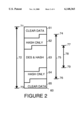
- FIG. 2 is a block diagram which shows partitioning of a data packet received by the circuit shown in FIG. 1 in accordance with a preferred embodiment of the present invention.
- FIG. 3 is a block diagram of a first-in-first-out (FIFO) buffer which functions as a dual pointer circular queue in accordance with a preferred embodiment of the present invention.
- FIFO first-in-first-out
- FIG. 4 is a diagram the first-in-first-out (FIFO) buffer which functions as a dual pointer circular queue shown in FIG. 3 in accordance with a preferred embodiment of the present invention.
- FIFO first-in-first-out
- FIG. 1 is a block diagram of a circuit which performs data encryption/decryption and hashing in accordance with a preferred embodiment of the present invention.
- a Data Encryption Standard (DES) processing block 32 includes a high speed ciphering engine that supports the Data Encryption Standard. See for example, Data Encryption Standard (DES), Federal Information Processing Standards Publication (FIPS PUB) 46-2, Dec. 30, 1993 available from the U.S. Department of Commerce, Technology Administration, National Institute of Standards and Technology. See also DES Modes of Operation, Federal Information Processing Standards Publication (FIPS PUB) 81, Dec. 2, 1980 available from the U.S. Department of Commerce, National Bureau of Standards. Alternatively, some other encryption/decryption algorithm may be used.
- DES Data Encryption Standard
- FIPS PUB Federal Information Processing Standards Publication
- a hash processing block 33 includes a hash engine which implements the FIPS 180-1 compliant Secure Hash Algorithm (SHA-1) and the MD5 has algorithm. These algorithms are used for computing condensed representations of a message or data filed, called a message digest. SHA-1 generates a 160-bit message digest while MD5 generates a 128-bit message digest.
- SHA-1 generates a 160-bit message digest
- MD5 generates a 128-bit message digest.
- the message digest is used during generation of a signature for the message. It is also used to compute a message digest for the received version of the message during the process of verifying the signature. Any change to the message in transit will, with very high probability, result in a different message digest, and the signature will fail to verify.
- the algorithm is designed to have the following properties: it is computationally infeasible to find a message which corresponds to a given message digest, or to find two different messages which produce the same digest.
- An in place buffer (IPB) 31 receives data over an SSRAM interface 20.
- IPB 31 generates a transmit ready (TXRDY) signal 21 and a receive ready (RXRDY) signal 22.
- RXRDY signal 22 will be high whenever there are at least eight word (32 byte) locations available in IPB 31. Otherwise RXRDY signal 22 will be low.
- TXRDY signal 21 will be low whenever there are at least eight word (32 byte) locations which include data that has been processed and is available to be read from available IPB 31. Otherwise TXRDY signal 21 will be low.
- a hash offset 35, a byte count 36 and an OPcode 17 are used as input to IPB 31. Also used as input are a DES Offset 38 and a DES length 39.
- Data in IPD 31 is output on a data path 23 and processed by DES processing block 32 and/or hash processing block 13.
- a multiplexer 34 selects data directly from IPD 31 or from an output 27 of DES processing block 31 to be forwarded to hash processing block 33.
- FIG. 2 is a block diagram which shows partitioning of a data packet 60 received by the circuit shown in FIG. 1.
- a beginning of packet 60 is represented by a line 71.
- An end of packet 60 is represented by a line 73.
- the total length of packet 60 is represented by arrows 72.
- a line 74 represents the location in packet 60 specified by hash offset 35.
- hash data 62 i.e., data which is subject to hashing but not to DES processing.
- a line 77 represents the location in packet 60 specified by hash offset 35.
- a line 79 represents the location in packet 60 specified by DES offset 38 plus DES length 39.
- An arrow 78 represents DES length 39.
- hash data 64 i.e., data which is subject to hashing but not to DES processing.
- a line 76 represents the location in packet 60 specified by hash offset 35 plus the hash length.
- An arrow 75 represents the hash length.
- IPD 31 operates as a first-in-first-out (FIFO) buffer which is implemented as a dual pointer circular queue.
- FIG. 3 illustrates how this is accomplished.
- Data from SSRAM interface 20 is written into IPD 31 to the location indicated by a write pointer 42.
- Write pointer 42 points to the location that will be written by the next data word (four bytes).
- Data is read out of IPD 31 using an input address (iaddr) pointer 44 to locate a next data word (four bytes) that will be processed.
- an output address (oaddr) pointer 43 is used to replace processed data back into IPD 31.
- SSRAM interface 20 then reads the processed information out of IPB 31 using a read pointer 41 which denotes the current position in the buffer.
- data locations 0, 1, 8, 9, 10, 11, 12, 13, 14 and 15 are empty of data.
- a data location 7 and a data location 6 a four byte word of data has been written and is ready for processing.
- a data location 5 and a data location 4 a four byte word of data has been read into either DES processing block 32 or hash processing block 33 and is being processed.
- a data location 3 and a data location 2 a four byte word of data has been processed and returned if required. After hashing the data need not be returned.
- read pointer 41 is actually stored. Instead of tracking the other pointers, read pointer 41 is used as a base in a circular queue and difference values are stored for each of the other pointers. This is illustrated by FIG. 4.
- circular queue 50 represents IPD 31.
- Write pointer 42, iaddr pointer 44, oaddr pointer 43 and read pointer 41 are shown as lines, positioned as shown.
- a difference value "done" is represented by an arrow 52. The difference value done is the number of four byte words in IPD 31 that have been processed and are available to be read.
- a difference value "process” is represented by an arrow 51.
- the difference value process is the number of four byte words in IPD 31 that are being processed.
- a difference value "delta” is represented by an arrow 53.
- the difference value delta is the number of four byte words in IPD 31 that are currently in use (i.e., not empty of data).
- each of the pointers can derived from read pointer 41 and the different values as follows:
- Write pointer 42 is located by adding the difference value delta to read pointer 41.
- the difference value delta is incremented when a four byte word is written into IPD 31 from SSRAM interface 20.
- the difference value delta is decremented when a four byte word is read from IPD 31 to SSRAM interface 20.
- Byte count 16 (shown in FIG. 1) is used to store the value of read pointer 41.
- Table 1 below gives an example of values for a difference value delta, a read pointer and a write pointer for accesses into a four word buffer.
- a four word buffer is used to simplify illustration of how a difference value is used to calculate the write pointer from the read pointer.
Abstract
Description
              TABLE 1
______________________________________
Access Type
          Read Pointer  Delta  Write Pointer
______________________________________
Reset     00            0 00   00
Write     00            0 01   01
Write     00            0 10   10
Read      01            0 01   10
Write     01            0 10   11
Write     01            0 11   00
Write     01            1 00   01
______________________________________
Claims (17)
Priority Applications (1)
| Application Number | Priority Date | Filing Date | Title |
|---|---|---|---|
| US09/107,030 US6148365A (en) | 1998-06-29 | 1998-06-29 | Dual pointer circular queue |
Applications Claiming Priority (1)
| Application Number | Priority Date | Filing Date | Title |
|---|---|---|---|
| US09/107,030 US6148365A (en) | 1998-06-29 | 1998-06-29 | Dual pointer circular queue |
Publications (1)
| Publication Number | Publication Date |
|---|---|
| US6148365A true US6148365A (en) | 2000-11-14 |
Family
ID=22314494
Family Applications (1)
| Application Number | Title | Priority Date | Filing Date |
|---|---|---|---|
| US09/107,030 Expired - Lifetime US6148365A (en) | 1998-06-29 | 1998-06-29 | Dual pointer circular queue |
Country Status (1)
| Country | Link |
|---|---|
| US (1) | US6148365A (en) |
Cited By (11)
| Publication number | Priority date | Publication date | Assignee | Title |
|---|---|---|---|---|
| US6411904B1 (en) * | 1998-05-14 | 2002-06-25 | Luminex Corporation | Zero dead time architecture for flow cytometer |
| US20030039354A1 (en) * | 2001-08-27 | 2003-02-27 | Kimble David E. | FIFO architecture with in-place cryptographic service |
| US20060230052A1 (en) * | 2005-04-12 | 2006-10-12 | Parama Networks, Inc. | Compact and hitlessly-resizable multi-channel queue |
| US20080016216A1 (en) * | 2006-04-03 | 2008-01-17 | Worley John S | Method and system for data-structure management |
| US20120054408A1 (en) * | 2010-08-31 | 2012-03-01 | Dong Yao Zu Eddie | Circular buffer in a redundant virtualization environment |
| US20120170768A1 (en) * | 2009-09-03 | 2012-07-05 | Robert Bosch Gmbh | Delay unit for a conference audio system, method for delaying audio input signals, computer program and conference audio system |
| US20130282961A1 (en) * | 2012-04-19 | 2013-10-24 | Kabushiki Kaisha Toshiba | Semiconductor memory device and method of control thereof |
| US20140181831A1 (en) * | 2012-12-20 | 2014-06-26 | Thomson Licensing | DEVICE AND METHOD FOR OPTIMIZATION OF DATA PROCESSING IN A MapReduce FRAMEWORK |
| US20160291868A1 (en) * | 2015-03-31 | 2016-10-06 | Kabushiki Kaisha Toshiba | Out of order sgl read sorting in a mixed system with prp read or system that supports only sgl reads |
| US10083127B2 (en) * | 2016-08-22 | 2018-09-25 | HGST Netherlands B.V. | Self-ordering buffer |
| CN114866343A (en) * | 2022-07-04 | 2022-08-05 | 支付宝(杭州)信息技术有限公司 | Data processing method and device |
Citations (2)
| Publication number | Priority date | Publication date | Assignee | Title |
|---|---|---|---|---|
| US5978868A (en) * | 1997-08-28 | 1999-11-02 | Cypress Semiconductor Corp. | System for generating buffer status flags by comparing read and write pointers and determining direction of progression of read pointer with respect to write pointer |
| US6003099A (en) * | 1995-03-22 | 1999-12-14 | Telefonaktiebolaget Lm Ericsson | Arrangement and method relating to handling of digital signals and a processing arrangement comprising such |
-
1998
- 1998-06-29 US US09/107,030 patent/US6148365A/en not_active Expired - Lifetime
Patent Citations (2)
| Publication number | Priority date | Publication date | Assignee | Title |
|---|---|---|---|---|
| US6003099A (en) * | 1995-03-22 | 1999-12-14 | Telefonaktiebolaget Lm Ericsson | Arrangement and method relating to handling of digital signals and a processing arrangement comprising such |
| US5978868A (en) * | 1997-08-28 | 1999-11-02 | Cypress Semiconductor Corp. | System for generating buffer status flags by comparing read and write pointers and determining direction of progression of read pointer with respect to write pointer |
Cited By (19)
| Publication number | Priority date | Publication date | Assignee | Title |
|---|---|---|---|---|
| US6411904B1 (en) * | 1998-05-14 | 2002-06-25 | Luminex Corporation | Zero dead time architecture for flow cytometer |
| US6658357B2 (en) | 1998-05-14 | 2003-12-02 | Luminex Corporation | Zero dead time architecture and method for flow cytometer |
| US20040098231A1 (en) * | 1998-05-14 | 2004-05-20 | Chandler Van S. | Zero dead time architecture and method for flow cytometer |
| US7047138B2 (en) | 1998-05-14 | 2006-05-16 | Luminex Corporation | Zero dead time architecture and method for flow cytometer |
| US20030039354A1 (en) * | 2001-08-27 | 2003-02-27 | Kimble David E. | FIFO architecture with in-place cryptographic service |
| US20060230052A1 (en) * | 2005-04-12 | 2006-10-12 | Parama Networks, Inc. | Compact and hitlessly-resizable multi-channel queue |
| US8176179B2 (en) * | 2006-04-03 | 2012-05-08 | Secure64 Software Corporation | Method and system for data-structure management |
| US20080016216A1 (en) * | 2006-04-03 | 2008-01-17 | Worley John S | Method and system for data-structure management |
| US20120170768A1 (en) * | 2009-09-03 | 2012-07-05 | Robert Bosch Gmbh | Delay unit for a conference audio system, method for delaying audio input signals, computer program and conference audio system |
| US9271096B2 (en) * | 2009-09-03 | 2016-02-23 | Robert Bosch Gmbh | Delay unit for a conference audio system, method for delaying audio input signals, computer program and conference audio system |
| US20120054408A1 (en) * | 2010-08-31 | 2012-03-01 | Dong Yao Zu Eddie | Circular buffer in a redundant virtualization environment |
| US8533390B2 (en) * | 2010-08-31 | 2013-09-10 | Intel Corporation | Circular buffer in a redundant virtualization environment |
| US20130282961A1 (en) * | 2012-04-19 | 2013-10-24 | Kabushiki Kaisha Toshiba | Semiconductor memory device and method of control thereof |
| US9442841B2 (en) * | 2012-04-19 | 2016-09-13 | Kabushiki Kaisha Toshiba | Semiconductor memory device and method for logging monitored events into a buffer |
| US20140181831A1 (en) * | 2012-12-20 | 2014-06-26 | Thomson Licensing | DEVICE AND METHOD FOR OPTIMIZATION OF DATA PROCESSING IN A MapReduce FRAMEWORK |
| US20160291868A1 (en) * | 2015-03-31 | 2016-10-06 | Kabushiki Kaisha Toshiba | Out of order sgl read sorting in a mixed system with prp read or system that supports only sgl reads |
| US9990138B2 (en) * | 2015-03-31 | 2018-06-05 | Toshiba Memory Corporation | Out of order SGL read sorting in a mixed system with PRP read or system that supports only SGL reads |
| US10083127B2 (en) * | 2016-08-22 | 2018-09-25 | HGST Netherlands B.V. | Self-ordering buffer |
| CN114866343A (en) * | 2022-07-04 | 2022-08-05 | 支付宝(杭州)信息技术有限公司 | Data processing method and device |
Similar Documents
| Publication | Publication Date | Title |
|---|---|---|
| US6295604B1 (en) | Cryptographic packet processing unit | |
| US6148365A (en) | Dual pointer circular queue | |
| US6457058B1 (en) | Network switch with hash table look up | |
| US6983366B1 (en) | Packet Processor | |
| US7366865B2 (en) | Enqueueing entries in a packet queue referencing packets | |
| JP2829807B2 (en) | Cell delay addition circuit | |
| KR101008510B1 (en) | Method, system, and computer program product for high-performance bonding resequencing | |
| US20090106500A1 (en) | Method and Apparatus for Managing Buffers in a Data Processing System | |
| US7327674B2 (en) | Prefetching techniques for network interfaces | |
| US7117308B1 (en) | Hypertransport data path protocol | |
| US8291138B2 (en) | Skip based control logic for first in first out buffer | |
| US20100005199A1 (en) | Direct memory access (dma) data transfers with reduced overhead | |
| US6480942B1 (en) | Synchronized FIFO memory circuit | |
| JP2002132677A (en) | Electronic mail transferring device and electronic mail device | |
| WO2019024763A1 (en) | Message processing | |
| US20060036817A1 (en) | Method and system for supporting memory unaligned writes in a memory controller | |
| US7870310B2 (en) | Multiple counters to relieve flag restriction in a multi-queue first-in first-out memory system | |
| KR20150077288A (en) | A look-aside processor unit with internal and external access for multicore processors | |
| JP2002342262A (en) | Direct memory access controller and direct memory access control method | |
| US6880050B1 (en) | Storage device, system and method which can use tag bits to synchronize queuing between two clock domains, and detect valid entries within the storage device | |
| US5896384A (en) | Method and apparatus for transferring deterministic latency packets in a ringlet | |
| US8688903B1 (en) | Associative list processing unit | |
| US8140792B2 (en) | Indirectly-accessed, hardware-affine channel storage in transaction-oriented DMA-intensive environments | |
| US6301264B1 (en) | Asynchronous data conversion circuit | |
| US11360911B2 (en) | Dummy data removal in an authenticated encryption with associated data cryptographic scheme |
Legal Events
| Date | Code | Title | Description |
|---|---|---|---|
| AS | Assignment |
Owner name: VLSI TECHNOLOGY, INC., CALIFORNIA Free format text: ASSIGNMENT OF ASSIGNORS INTEREST;ASSIGNOR:BUER, MARK LEONARD;REEL/FRAME:009299/0222 Effective date: 19980623 |
|
| STCF | Information on status: patent grant |
Free format text: PATENTED CASE |
|
| FPAY | Fee payment |
Year of fee payment: 4 |
|
| AS | Assignment |
Owner name: NXP B.V., NETHERLANDS Free format text: ASSIGNMENT OF ASSIGNORS INTEREST;ASSIGNOR:PHILIPS SEMICONDUCTORS INC.;REEL/FRAME:018645/0779 Effective date: 20061130 Owner name: PHILIPS SEMICONDUCTORS VLSI INC., NEW YORK Free format text: CHANGE OF NAME;ASSIGNOR:VLSI TECHNOLOGY, INC.;REEL/FRAME:018635/0570 Effective date: 19990702 |
|
| AS | Assignment |
Owner name: PHILIPS SEMICONDUCTORS INC., NEW YORK Free format text: CHANGE OF NAME;ASSIGNOR:PHILIPS SEMICONDUCTORS VLSI INC.;REEL/FRAME:018668/0255 Effective date: 19991220 |
|
| FPAY | Fee payment |
Year of fee payment: 8 |
|
| FPAY | Fee payment |
Year of fee payment: 12 |
|
| AS | Assignment |
Owner name: PARTNERS FOR CORPORATE RESEARCH INTERNATIONAL, CAY Free format text: ASSIGNMENT OF ASSIGNORS INTEREST;ASSIGNOR:NXP B. V.;REEL/FRAME:031334/0449 Effective date: 20120907 |
|
| AS | Assignment |
Owner name: FUTURE LINK SYSTEMS, CALIFORNIA Free format text: ASSIGNMENT OF ASSIGNORS INTEREST;ASSIGNOR:PARTNERS FOR CORPORATE RESEARCH INTERNATIONAL;REEL/FRAME:032399/0965 Effective date: 20130808 |