US6147935A - Transformerless LED digital alarm clock - Google Patents
Transformerless LED digital alarm clock Download PDFInfo
- Publication number
- US6147935A US6147935A US09/451,492 US45149299A US6147935A US 6147935 A US6147935 A US 6147935A US 45149299 A US45149299 A US 45149299A US 6147935 A US6147935 A US 6147935A
- Authority
- US
- United States
- Prior art keywords
- power
- output
- voltage
- rectifier
- digital clock
- Prior art date
- Legal status (The legal status is an assumption and is not a legal conclusion. Google has not performed a legal analysis and makes no representation as to the accuracy of the status listed.)
- Expired - Fee Related
Links
Images

Classifications
-
- G—PHYSICS
- G04—HOROLOGY
- G04G—ELECTRONIC TIME-PIECES
- G04G19/00—Electric power supply circuits specially adapted for use in electronic time-pieces
- G04G19/10—Arrangements for supplying back-up power
-
- G—PHYSICS
- G04—HOROLOGY
- G04C—ELECTROMECHANICAL CLOCKS OR WATCHES
- G04C10/00—Arrangements of electric power supplies in time-pieces
-
- H—ELECTRICITY
- H02—GENERATION; CONVERSION OR DISTRIBUTION OF ELECTRIC POWER
- H02M—APPARATUS FOR CONVERSION BETWEEN AC AND AC, BETWEEN AC AND DC, OR BETWEEN DC AND DC, AND FOR USE WITH MAINS OR SIMILAR POWER SUPPLY SYSTEMS; CONVERSION OF DC OR AC INPUT POWER INTO SURGE OUTPUT POWER; CONTROL OR REGULATION THEREOF
- H02M7/00—Conversion of AC power input into DC power output; Conversion of DC power input into AC power output
- H02M7/02—Conversion of AC power input into DC power output without possibility of reversal
- H02M7/04—Conversion of AC power input into DC power output without possibility of reversal by static converters
- H02M7/05—Capacitor coupled rectifiers
Definitions
- the present invention relates to clocks and clock radios, and more specifically to a transformerless LED digital alarm clock and LED clock radios using AC line voltage as a primary source of power which is converted to low voltage DC power useful for both running the clock and charging a backup battery.
- the digital clock uses a programmable microprocessor to provide the display control signals for four individual digit displays such that the "ON" time or duty cycle for each digit begin displayed is at a minimum.
- U.S. Pat. No. 4,697,930 to Roberts et al. and entitled "Transformerless Clock Circuit With Duplex Optoelectronic Display” discloses a transformerless power supply and display energizing circuit for a clock circuit with a duplex optoelectronic display driven by low voltage integrated clock circuit.
- the clock circuit has positive and negative voltage input terminals and the duplex display has a first terminal connected to a first common cathode and a second terminal connected to a second common cathode of the display.
- the transformerless circuit is powered from an AC source.
- An impedance which may be either resistive or reactive, reduces the AC voltage to a level suitable for the integrated clock circuit.
- the transformerless circuit also generates synchronous DC level-shifted pulse trains for driving the positive input terminal of the integrated clock circuit alternately between a first voltage and a reference voltage while synchronously driving the display first terminal between the first voltage and a voltage of equal amplitude and opposite polarity.
- U.S. Pat. No. 4,595,861 issued to Simopoulos et al. and entitled "Power Supplies for Electroluminescent Panels" discloses circuitry for converting a DC power supply to an AC power supply for electroluminescent lamps which are selfinhibited from further oscillations and are current limited in the event that a failure occurs in an EL (electroluminescent) lamp which results in the EL lamp being shorted.
- a single ended and push/pull transformer power supply is disclosed and according to a second embodiment, a transformerless solid state power supply is disclosed.
- the solid state power supply uses a voltage multiplier to increase the AC or square wave voltage to a level of almost 140 volts for powering the EL lamp.
- circuitry in this patent discloses techniques for converting from DC power to AC power, not AC power to DC power and further provides circuitry to inhibit oscillations and operations of the circuitry in the event of a shorting of the EL lamp or a substantial voltage drop.
- U.S. Pat. No. 4,201,039, to Roland M. Marion and entitled "Numerical Display Using Plural Light Sources and Having a Reduced and Substantially Constant Current Requirement” discloses a numerical digital display having a reduced DC current requirement per character display site.
- the circuitry is useful for powering a digital display in an AC powered clock or clock radio in which it is desirable to keep the DC current requirement of the display to a substantially constant minimum suitable for use with a low cost transformerless power supply conventional with radio receivers.
- the current requirements of the digital character display site is reduced over that of full parallel operation by selectively serializing certain light sources in a manner leaving the display control circuitry uncomplicated by permitting each light source state to be controlled by a shunt control switch sharing a common bus.
- the shunt control which diverts rather than prevents current flow in the display, allows the display current to remain substantially constant irrespective of the digital numbers displayed.
- U.S. Pat. No. 4,109,180 to Ogle et al., and entitled "AC-Powered Display System With Voltage Limitation” discloses an AC-powered display system which includes a gas discharge display panel, an integrated circuit, and a limiting network.
- the integrated circuit is provided as a display pattern controller and may also comprise a digital alarm clock circuitry which provides outputs for controlling the gas discharge display panel.
- the circuitry also includes a limiting network which reduces the current through the system in response to an excessive voltage across the controller.
- U.S. Pat. No. 4,063,234 to Arn et al. and entitled “Incandescent, Flat Screen, Video Display” discloses a flat screen video display comprising a plurality of incandescent lamps arranged in an addressable X-Y matrix.
- the circuitry also provides a memory and driver circuit for each individual incandescent lamp for use in a flat screen video display apparatus.
- U.S. Pat. No. 3,602,795 to John B. Gunn and entitled “Transformerless Power Supply” discloses circuits for converting an input voltage from a high amplitude to a lower amplitude DC voltage.
- the power supply portion of the clock circuitry comprises a pair of line terminals for receiving a source of the single phase AC power having a line voltage level of between about 100 and about 225 volts (for clocks used in Europe and other parts of the world).
- the AC power is rectified by standard rectifier circuitry such as by a full wave bridge rectifier.
- a voltage divider circuitry is connected between one of the line terminal and one of the inputs of the rectifier for substantially reducing the AC voltage seen by the rectifier to some value of less than about 15 volts.
- the rectifier includes a positive output and a negative output and has a capacitor connected across said outputs to filter or smooth the rectified power.
- a diode circuitry is connected across the positive and negative outputs of the rectifier to clamp the rectified and filtered power output at a DC voltage of between about 3.6 VDC and about 5 VDC for use as the low voltage DC power supply.
- the diode circuitry comprises a zener diode wherein the cathode end of the zener diode is connected to the positive output of the rectifier and the anode end of the zener diode is connected to the negative output of the rectifier.
- a positive DC output terminal is connected to the positive output of the rectifier and a negative DC output terminal is connected to the negative output of the rectifier.
- a source of clocking pulse is provided by any suitable source such as a crystal oscillator circuit or by synchronizing with the AC line voltage.
- the positive and negative terminals of a microprocessor suitable for providing four cathode outputs at four separate non-overlapping predetermined periods of time are connected to the positive and negative DC output terminals of the rectifier circuitry respectively.
- the microprocessor also provides at least seven anode outputs.
- the four cathode outputs and the seven anode outputs are used to individually control four separate LED digital displays at reduced duty cycles. At least two of the displays are capable of displaying all of the ten possible digits (0-9).
- the circuitry further includes a NiCad (Nickel Cadmium) rechargeable battery connected to the positive and negative DC output terminals for receiving a charging current.
- a blocking diode is included which has its anode connected to the positive output of the rectifier and its cathode connected to the positive DC output terminal of the battery such that a loss of AC line voltage will not result in the discharge of the battery.
- the present circuitry can also be used to operate a clock radio.
- the alarm or radio is connected between the positive and negative outputs of the rectifier circuit through a switch.
- the switch may be an electronic switch such as a bipolar diode which is turned on by an output from the microprocessor at the selected time.
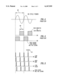
- FIG. 1 is a circuit diagram of a prior art transformerless LED digital clock using a commercially available Integrated Circuit (IC), i.e., clock circuit and including an LED duplex clock display;
- IC Integrated Circuit
- FIG. 2 illustrates a 60 cycle commercial power sine wave
- FIG. 3 shows the duty cycle for power applied to the digital clock display of the prior art circuit of FIG. 1 as it relates to the 60 cycle power of FIG. 2;
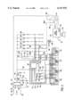
- FIG. 4 is an embodiment of circuit diagram of the LED digital clock and display incorporating the present invention.
- FIG. 5 comprises the duty cycle for power applied to the digital clock display of the embodiment of FIG. 4.
- FIG. 1 there is shown a typical digital clock with an LED digital display.
- the clock circuitry utilizes a conventional clock IC 12 and LED display panel 14.
- Plug 16 is a conventional AC plug having two prongs 18 and 20. With prong 20 connected to the reference or grounded side of the AC, while prong 18 is connected to the "hot" side. Thus, prong 20 will remain at a constant reference voltage while the AC voltage at prong 18 will alternately change polarity.
- Impedance element 22 is typically a capacitor 24 with a known impedance at the AC input frequency. The value of capacitance is chosen to give a desired reduction in the 115 VAC input power. Impedance element 22 would be a resistive impedance, however, an advantage of using a capacitive impedance such as capacitor 24 to reduce the input voltage is that, unlike a voltage-dropping resistor, the capacitor does not dissipate power. Therefore, there is little to no power loss or heat generated from the reactive impedance element.
- the reduced AC voltage from capacitor 24 forms one input to a full-wave bridge rectifier 26 which consists of diodes 28, 30, 32 and 34 connected in the well-known bridge rectifier configuration.
- the other input of bridge rectifier 26 is returned to the reference terminal 20 of plug 16 via a current limiting resistor 36.
- the full-wave rectified AC voltage at the output terminals of bridge rectifier 26 form the input to voltage regulator circuit 38, which consists of capacitor 40 and voltage regulating zener diode 42.
- Voltage regulating circuit 38 smooths and regulates the full-wave rectified output of bridge rectifier 26 in a well-known manner.
- the regulated output voltage from regulating circuit 38 is applied to the positive terminal 44 and the negative terminal 46 of clock IC 12. Assuming diode 42 is a 12-volt diode, the difference in voltage between the +V (44) and -V (46) inputs to clock IC 12 will be 12 VDC.
- Clock IC 12 is connected to LED display panel 14 in a known manner. However, the AC synchronizing input 48 to clock IC 12 is connected to the reference terminal 20 of the AC input via resistors 36 and 50. Thus, the AC synchronizing input to the clock IC 12 does not fluctuate but is held at the reference voltage.
- a first terminal "common 1" having reference number 41 is connected through diode 43 and resistor 45 to the positive input of rectifier bridge 36.
- a second terminal “common 2" having a reference number 47 is connected through diode 49 and resistor 51 to the negative or reference input to rectifier bridge 36.
- Terminals 41 and 47 are connected one each to the two sets of cathodes of the duplex four digit display 14.
- FIG. 2 there is shown a typical sine wave representing 60 cycle 120 VAC power commercially available in the United States.
- the period of the 60 cycle time wave is 16.67 milliseconds as shown by the double-headed arrow 52.
- each half cycle is approximately 8.33 milliseconds or one half of the total cycle time of a single sine wave.
- FIG. 3 there are shown representations of the time periods power is supplied to each of the four (4) LED displays discussed with respect to the prior art circuitry of FIG. 1.
- the graphs of FIGS. 3A and 3B are correlated with the sine wave of FIG. 2, and as can be seen, each of the "on" periods represented by the shaded areas are substantially equivalent to one half of a sine wave or approximately 8.3 milliseconds as indicated by double-headed arrow 54 of FIG. 3A.
- the graph of FIG. 3A represents both the "low minutes” (i.e., minutes 0 through 9), and the "high minutes” (0 through 59).
- 3B may be chosen to represent the "low hours” (0 through 9) and the "high hour” “1” (also perhaps 2 if a 24 hours clock is used), an alarm indicator and an AM or PM indicator.
- substantially half of the LED's will always be “on.” This is in contrast to the very low duty cycle for the "on" time of the LED's of the present invention which is shown as also being coordinated with the 60 cycle sine wave of FIG. 2 and which will be discussed in detail hereinafter.
- FIG. 4 there is shown a first embodiment of transformerless circuitry for powering an LED digital alarm clock according to the teachings of the present invention.
- a pair of terminals 60 and 62 for receiving normal line AC voltage such as 115 VAC.
- line voltage such as 115 VAC.
- 115 volts may be considered the nominal voltage for most power sources in the United States, it is not unusual that line voltage varies 5 to 10 volts to provide more or less voltage. Further, other countries such as the continent of Europe, typically use a 220 volt supply as standard power.
- the concept of the circuitry shown in FIG. 4 would be suitable for use with either nominal 115 VAC or nominal 220 VAC and slight variations of both. However, in the described embodiment, some of the elements making up the circuit are specifically designed for the U.S. 115 VAC nominal voltage average.
- the two input terminals 60 and 62 are connected as inputs to a rectifier circuitry 64.
- a resistor 66 and a capacitor 68 are connected as a voltage divider series circuit that prevents the resistor 66 from dropping essentially the entire AC voltage, and in fact most of the voltage is dropped across the capacitor 68.
- Capacitor 68 should have a voltage rating of at least 1.5 times the line voltage. However, as will be discussed in more detail later and as is indicated in FIG. 5, each of the four separate digits of the present invention are on for only 0.4 milliseconds as indicated by double-headed arrow 70 or a total of 0.16 milliseconds per half cycle of the AC voltage sine wave for all four digits.
- the total on time represents a duty cycle of about 4% compared to 100% duty cycle for the prior art circuit of FIG. 1.
- the current rating of the voltage-dropping capacitor 68 can be significantly reduced. This, of course, also allows for a significant reduction in physical size.
- the resistor 66 and the capacitor 68 will drop the input to the rectifier circuit 64 from the 115 VAC to around 100 volts or less, and for the embodiment of FIG. 1, these elements are chosen to be about 100 ohms and 0.47 ⁇ F respectively.
- Rectifier circuit 64 also includes a positive output on line 72 and a negative output on line 74 which, in the embodiment shown, is connected to ground 76. Any suitable rectifier circuit may be used in this invention however a full bridge rectifier such as made up by the diodes 78, 80, 82 and 84 are effective and readily available.
- a filter capacitor 86 is connected across the output lines 72 and 74 of the rectifier. Filter capacitor 86 is chosen to have a capacitance of about 1000 ⁇ F for the embodiment of FIG. 1.
- a diode circuit 88 which is connected across the positive/negative outputs 72 and 74 respectively of the rectifier so as to provide a clamped voltage output, which clamped voltage output as was discussed above is smoothed by filter capacitor 86.
- the voltage output of the rectifier circuitry 64 is clamped at a voltage of about 5.1 VDC so as to be useful as a low voltage DC power source for powering low current DC devices.
- a zener diode 90 may be chosen to clamp the voltage at the desired level such as is shown in the dashed line box 88.
- a series of voltage-dropping dividers connected anode to cathode may be used with the first diode of the series having its anode connected to line 72 and the last diode of the series with its cathode connected to line 74.
- a rechargeable battery such as a NiCad (Nickel Cadmium) battery 92 is also connected across the clamped filtered voltage provided by the diode circuitry 64 and capacitor 86.
- a blocking diode 94 with its anode connected to the positive output of the rectified voltage and its cathode connected to a positive terminal 96 of the NiCad battery.
- Blocking diode 94 prevents the battery from bleeding current back into the power supply and rectifier circuit 64 in the event of a line AC voltage power failure.
- the blocking diode 94 also further drops the supply voltage down to approximately 3.8 volts.
- the positive terminal of the microprocessor 98 is connected through line 99 to the positive terminal 96 of battery 92 and the negative terminal is connected to ground 76.
- an oscillator circuitry 100 for providing clocking pulses to microprocessor 98 as shown.
- Oscillator circuitry 100 includes a 0.4 mHz, crystal 102 and a pair of capacitors 104a and 104b connected across crystal 102 to maintain oscillation of the circuitry.
- capacitors 104a and 104b are each about 33 pico farads.
- a rechargeable vented Nickel Cadmium battery is particularly useful.
- the Nickel Cadmium batteries can allow for a continuous and safe overcharging without getting overheated. This is unlike other types of unvented batteries such as Nickel Metal Hydride or Lithium batteries which tend to overheat when they are overcharged. If batteries other than the Nickel Cadmium type are chosen, a thermistor circuit or other form of charge control circuitry well known in the art should be added to disconnect the battery from the charging circuit when the battery is fully charged to avoid overheating or damage to the batteries and/or the clock circuitry.
- the present invention uses a commercially available microprocessor 98 programmed and connected to provide four cathode outputs for each of the four individual LED digital displays 106, 108, 110 and 112.
- the microprocessor 98 also will provide a minimum of seven anode outputs to the LED display such that each of the seven segments in a common seven segment digital display can be individually controlled.
- generating seven anode outputs was normal with the prior art dedicated clock IC's, these dedicated IC's provide only two cathode outputs such that one half of the display or two of the digits are illuminated at a time as was discussed above with respect to FIGS. 3A and 3B.
- the "quad" or "four common" display of the present invention is made possible by the four separate cathode outputs of the microprocessor 98 and allows each one of the individual digital displays to be individually energized for any selected amount of time.
- the complete power management and overall power reduction of the present invention is achieved.
- the four individually controlled cathode outputs 114, 116, 118 and 120 are provided to the individual digital digit displays 106, 108, 110 and 112 respectively.
- microprocessor 98 further includes outputs on lines 122, 124, 126, 128, 130, 132 and 134, each of which is routed to each of the four digital displays 106, 108, 110 and 112.
- each digital display is capable of controlling each of the seven segments of a seven segment digital indicator.
- Dropping resistors 136 through 148 are located in each of the anode lines 122 through 134 to prevent excessive current draw in case of a display failure. In the embodiment shown in FIG. 4, resistors 136 through 148 are each chosen to be at about 10 ohms.
- buttons 150 through 158 for setting the time of the clock, for setting the alarm time on the clock, for causing an increase of the alarm or time set, and a button for causing the decrease of the alarm or time set as indicated by buttons 150, 152, 154 and 156 respectively.
- Button 158 represents the control for turning the alarm ON or OFF.
- Each of the switches receive power from the cathode of diode 94 and/or battery 92 and are connected to a voltage divider comprised of a pair of resistors such as resistors 160 and 162 shown with respect to switch 150.
- the two resistors are chosen in the present embodiment to have values of 820 ohms and 2.2 kohms respectively.
- Each of the other four switches 152, 154, 156 and 158 have similar voltage dividing circuitries made up of similar resistors. Each of the nodes between the two resistors 160 and 162 are provided as control inputs to microprocessor 98 and to each of the individual digital indicators 106 through 112.
- microprocessor 98 further provides an output to loudspeaker 164 by means of line 166.
- microprocessor 98 will generate an electrical signal in the audible range and preferably at about 400 Hz which will act as a buzzer or alarm.
- the output on line 166 to the speaker 164 will occur in response to the alarm set time being reached on the clock.
- the buzzer or alarm OFF the user will hit the ALARM ON/OFF button 158 discussed heretofore.
- the circuitry discussed provides for an alarm clock with a buzzer or other generated noise used as an alarm. However, it will be appreciated that most people prefer to be awakened by music such as by a clock radio.
- a switch member 168 connected to sound circuitry 170. Also, as shown, the negative side of sound circuitry 170 is connected to ground 76.
- the switch 168 is typically an electronic switch such as a "PNP" transistor which is turned on by a trigger signal to the base 172 of the transistor 174 at the set alarm time.
- the trigger signal to base 172 of ON and OFF power transistor 174 is from microprocessor 98 on line 166 and the extension of line 166 shown by the dashed line portion 166a.
- Sound circuitry 170 is shown having a speaker 176 for converting the electrical signals representative of sound to audible signals which will be heard by the user. Sound circuitry 170 could also be a buzzer, but preferably, as discussed above, is a radio receiver, a CD player or other type of music making device, or even an IC chip which makes different and pleasant sounds.
- volume control 178 which is typically required for the radio receiver, but may also be used for the sound provided by an integrated circuit or even the strident sound of a buzzer. As shown, the power output to the sound circuitry 170 will be the 3.6 volts across the zener diode 36.
Landscapes
- Engineering & Computer Science (AREA)
- Power Engineering (AREA)
- Physics & Mathematics (AREA)
- General Physics & Mathematics (AREA)
- Electric Clocks (AREA)
Abstract
Description
Claims (15)
Priority Applications (2)
| Application Number | Priority Date | Filing Date | Title |
|---|---|---|---|
| US09/451,492 US6147935A (en) | 1999-11-30 | 1999-11-30 | Transformerless LED digital alarm clock |
| CA002327129A CA2327129A1 (en) | 1999-11-30 | 2000-11-30 | Transformerless led digital alarm clock |
Applications Claiming Priority (1)
| Application Number | Priority Date | Filing Date | Title |
|---|---|---|---|
| US09/451,492 US6147935A (en) | 1999-11-30 | 1999-11-30 | Transformerless LED digital alarm clock |
Publications (1)
| Publication Number | Publication Date |
|---|---|
| US6147935A true US6147935A (en) | 2000-11-14 |
Family
ID=23792440
Family Applications (1)
| Application Number | Title | Priority Date | Filing Date |
|---|---|---|---|
| US09/451,492 Expired - Fee Related US6147935A (en) | 1999-11-30 | 1999-11-30 | Transformerless LED digital alarm clock |
Country Status (2)
| Country | Link |
|---|---|
| US (1) | US6147935A (en) |
| CA (1) | CA2327129A1 (en) |
Cited By (13)
| Publication number | Priority date | Publication date | Assignee | Title |
|---|---|---|---|---|
| US20030142591A1 (en) * | 2002-01-31 | 2003-07-31 | International Business Machines Corporation | Interactive alarm clock and method |
| US20060153010A1 (en) * | 2002-05-24 | 2006-07-13 | Keith Kibiloski | Radio-controlled clock |
| US20060229746A1 (en) * | 2005-04-07 | 2006-10-12 | Ollis Jeffrey D | Modular controller for an environmental management system |
| US20070067300A1 (en) * | 2005-09-16 | 2007-03-22 | Ollis Jeffrey D | Network alarm clock communicating alarm settings over a wireless or other local area network |
| US20070063832A1 (en) * | 2005-09-16 | 2007-03-22 | Ollis Jeffrey D | Method and apparatus for using a wireless controller in a wired security system |
| US7602158B1 (en) * | 2005-03-21 | 2009-10-13 | National Semiconductor Corporation | Power circuit for generating non-isolated low voltage power in a standby condition |
| CN101667011B (en) * | 2009-08-14 | 2011-03-16 | 深圳市强大实业有限公司 | Alternating current power supply electronic clock with power saving structure |
| CN103023353A (en) * | 2012-12-27 | 2013-04-03 | 常州大学 | Multi-output digital display power source |
| US20140361623A1 (en) * | 2012-01-20 | 2014-12-11 | Osram Sylvania Inc. | Auxiliary power supply for lighting driver circuitry |
| US20150207424A1 (en) * | 2014-01-23 | 2015-07-23 | Panasonic Intellectual Property Management Co., Ltd. | Switching power supply and electric power converter |
| US9922547B2 (en) * | 1998-07-22 | 2018-03-20 | Touchtunes Music Corporation | Remote control unit for activating and deactivating means for payment and for displaying payment status |
| CN111258208A (en) * | 2020-03-08 | 2020-06-09 | 东华理工大学 | An embedded intelligent digital clock |
| US11394480B2 (en) * | 2019-08-23 | 2022-07-19 | Bose Corporation | Systems and methods for synchronizing device clocks |
Citations (3)
| Publication number | Priority date | Publication date | Assignee | Title |
|---|---|---|---|---|
| US4198629A (en) * | 1977-06-06 | 1980-04-15 | General Electric Company | Numerical display using plural light sources and having a reduced and substantially constant current requirement |
| US4201039A (en) * | 1977-06-06 | 1980-05-06 | General Electric Company | Numerical display using plural light sources and having a reduced and substantially constant current requirement |
| US4697930A (en) * | 1986-07-03 | 1987-10-06 | Spartus Corporation | Transformerless clock circuit with duplex optoelectronic display |
-
1999
- 1999-11-30 US US09/451,492 patent/US6147935A/en not_active Expired - Fee Related
-
2000
- 2000-11-30 CA CA002327129A patent/CA2327129A1/en not_active Abandoned
Patent Citations (3)
| Publication number | Priority date | Publication date | Assignee | Title |
|---|---|---|---|---|
| US4198629A (en) * | 1977-06-06 | 1980-04-15 | General Electric Company | Numerical display using plural light sources and having a reduced and substantially constant current requirement |
| US4201039A (en) * | 1977-06-06 | 1980-05-06 | General Electric Company | Numerical display using plural light sources and having a reduced and substantially constant current requirement |
| US4697930A (en) * | 1986-07-03 | 1987-10-06 | Spartus Corporation | Transformerless clock circuit with duplex optoelectronic display |
Cited By (17)
| Publication number | Priority date | Publication date | Assignee | Title |
|---|---|---|---|---|
| US9922547B2 (en) * | 1998-07-22 | 2018-03-20 | Touchtunes Music Corporation | Remote control unit for activating and deactivating means for payment and for displaying payment status |
| US20030142591A1 (en) * | 2002-01-31 | 2003-07-31 | International Business Machines Corporation | Interactive alarm clock and method |
| US20060153010A1 (en) * | 2002-05-24 | 2006-07-13 | Keith Kibiloski | Radio-controlled clock |
| US7385879B2 (en) * | 2002-05-24 | 2008-06-10 | Equity Industries, Inc. | Radio-controlled clock |
| US7602158B1 (en) * | 2005-03-21 | 2009-10-13 | National Semiconductor Corporation | Power circuit for generating non-isolated low voltage power in a standby condition |
| US20060229746A1 (en) * | 2005-04-07 | 2006-10-12 | Ollis Jeffrey D | Modular controller for an environmental management system |
| US20070067300A1 (en) * | 2005-09-16 | 2007-03-22 | Ollis Jeffrey D | Network alarm clock communicating alarm settings over a wireless or other local area network |
| US20070063832A1 (en) * | 2005-09-16 | 2007-03-22 | Ollis Jeffrey D | Method and apparatus for using a wireless controller in a wired security system |
| CN101667011B (en) * | 2009-08-14 | 2011-03-16 | 深圳市强大实业有限公司 | Alternating current power supply electronic clock with power saving structure |
| US9859812B2 (en) * | 2012-01-20 | 2018-01-02 | Osram Sylvania Inc. | Auxiliary power supply for lighting driver circuitry |
| US20140361623A1 (en) * | 2012-01-20 | 2014-12-11 | Osram Sylvania Inc. | Auxiliary power supply for lighting driver circuitry |
| CN103023353A (en) * | 2012-12-27 | 2013-04-03 | 常州大学 | Multi-output digital display power source |
| CN103023353B (en) * | 2012-12-27 | 2015-08-26 | 常州大学 | A kind of multi output digital display power supply |
| US9431917B2 (en) * | 2014-01-23 | 2016-08-30 | Panasonic Intellectual Property Management Co., Ltd. | Switching power supply including a rectifier circuit having switching elements, and electric power converter |
| US20150207424A1 (en) * | 2014-01-23 | 2015-07-23 | Panasonic Intellectual Property Management Co., Ltd. | Switching power supply and electric power converter |
| US11394480B2 (en) * | 2019-08-23 | 2022-07-19 | Bose Corporation | Systems and methods for synchronizing device clocks |
| CN111258208A (en) * | 2020-03-08 | 2020-06-09 | 东华理工大学 | An embedded intelligent digital clock |
Also Published As
| Publication number | Publication date |
|---|---|
| CA2327129A1 (en) | 2001-05-30 |
Similar Documents
| Publication | Publication Date | Title |
|---|---|---|
| US6147935A (en) | Transformerless LED digital alarm clock | |
| US5982105A (en) | Transformerless electroluminescent lamp driver topology | |
| US5502357A (en) | Low cost inverter for EL lamp | |
| JP2000232241A (en) | Lighting electronic device and lighting method | |
| US4956826A (en) | Multi-year time clock having automatic daylight saving time compensator | |
| US4409439A (en) | Controllable telephone call annunciator | |
| US7433274B1 (en) | Rapid set handicapped alarm clock | |
| CA2327173A1 (en) | Transformerless quartz analog clock | |
| AU601933B2 (en) | Paging receiver with a light emitting flashing circuit | |
| US4006583A (en) | Electronic display device for timepiece and the like | |
| EP0256642A2 (en) | Transformerless power supply circuit for a clock circuit | |
| CN110673460B (en) | User testable thermoelectric watch | |
| GB2386207A (en) | Silent anatomic alarm system | |
| KR920000751Y1 (en) | Timer device for midnight power supply | |
| CN2393126Y (en) | Light emitting diode digital clock | |
| EP0277798A2 (en) | Speaker Driver | |
| JP2532165B2 (en) | Low frequency therapy device | |
| JPS5943797Y2 (en) | load drive circuit | |
| GB2422447A (en) | Dawn simulator alarm clock | |
| JPS6146468Y2 (en) | ||
| JPS6210718Y2 (en) | ||
| JPS6041753B2 (en) | electronic timer device | |
| JPS6388491A (en) | Separate timer | |
| HK40019463A (en) | User-testable termoelectric watch | |
| JP2983582B2 (en) | Charging system |
Legal Events
| Date | Code | Title | Description |
|---|---|---|---|
| AS | Assignment |
Owner name: GTC PROPERTIES, INC., DELAWARE Free format text: ASSIGNMENT OF ASSIGNORS INTEREST;ASSIGNORS:GUYETT, THOMAS G.;REEVES, MICHAEL H.;HOBBS, STEPHEN B.;REEL/FRAME:010569/0731;SIGNING DATES FROM 20000131 TO 20000207 |
|
| AS | Assignment |
Owner name: FLEET CAPITAL CORPORATION, AS AGENT, GEORGIA Free format text: ASSIGNMENT OF ASSIGNORS INTEREST;ASSIGNOR:GTC PROPERTIES, INC.;REEL/FRAME:011590/0614 Effective date: 20010215 |
|
| AS | Assignment |
Owner name: SALTON, INC., ILLINOIS Free format text: ASSIGNMENT OF ASSIGNORS INTEREST;ASSIGNOR:GTC PROPERTIES, INC.;REEL/FRAME:012090/0926 Effective date: 20010807 |
|
| AS | Assignment |
Owner name: WACHOVIA BANK, NATIONAL ASSOCIATION, GEORGIA Free format text: SECURITY AGREEMENT;ASSIGNORS:SALTON, INC.;TOASTMASTER, INC.;SALTON TOASTMASTER LOGISTICS LLC;AND OTHERS;REEL/FRAME:014108/0719 Effective date: 20030509 |
|
| REMI | Maintenance fee reminder mailed | ||
| AS | Assignment |
Owner name: WELLS FARGO FOOTHILL, INC., CALIFORNIA Free format text: SECURITY INTEREST;ASSIGNOR:WACHOVIA BANK NATIONAL ASSOCIATION;REEL/FRAME:015127/0865 Effective date: 20040830 |
|
| LAPS | Lapse for failure to pay maintenance fees | ||
| LAPS | Lapse for failure to pay maintenance fees |
Free format text: PATENT EXPIRED FOR FAILURE TO PAY MAINTENANCE FEES (ORIGINAL EVENT CODE: EXP.); ENTITY STATUS OF PATENT OWNER: LARGE ENTITY |
|
| STCH | Information on status: patent discontinuation |
Free format text: PATENT EXPIRED DUE TO NONPAYMENT OF MAINTENANCE FEES UNDER 37 CFR 1.362 |
|
| FP | Lapsed due to failure to pay maintenance fee |
Effective date: 20041114 |
|
| AS | Assignment |
Owner name: THE BANK OF NEW YORK (AS ADMINISTRATIVE AND COLLAT Free format text: SECURITY AGREEMENT;ASSIGNORS:SALTON, INC.;TOASTMASTER INC.;SALTON TOASTMASTER LOGISTICS LLC;AND OTHERS;REEL/FRAME:016761/0797 Effective date: 20050826 |