US6147387A - Static random access memory - Google Patents
Static random access memory Download PDFInfo
- Publication number
- US6147387A US6147387A US09/116,889 US11688998A US6147387A US 6147387 A US6147387 A US 6147387A US 11688998 A US11688998 A US 11688998A US 6147387 A US6147387 A US 6147387A
- Authority
- US
- United States
- Prior art keywords
- resistance
- random access
- static random
- access memory
- insulating film
- Prior art date
- Legal status (The legal status is an assumption and is not a legal conclusion. Google has not performed a legal analysis and makes no representation as to the accuracy of the status listed.)
- Expired - Fee Related
Links
Images


Classifications
-
- H—ELECTRICITY
- H10—SEMICONDUCTOR DEVICES; ELECTRIC SOLID-STATE DEVICES NOT OTHERWISE PROVIDED FOR
- H10B—ELECTRONIC MEMORY DEVICES
- H10B10/00—Static random access memory [SRAM] devices
- H10B10/15—Static random access memory [SRAM] devices comprising a resistor load element
-
- Y—GENERAL TAGGING OF NEW TECHNOLOGICAL DEVELOPMENTS; GENERAL TAGGING OF CROSS-SECTIONAL TECHNOLOGIES SPANNING OVER SEVERAL SECTIONS OF THE IPC; TECHNICAL SUBJECTS COVERED BY FORMER USPC CROSS-REFERENCE ART COLLECTIONS [XRACs] AND DIGESTS
- Y10—TECHNICAL SUBJECTS COVERED BY FORMER USPC
- Y10S—TECHNICAL SUBJECTS COVERED BY FORMER USPC CROSS-REFERENCE ART COLLECTIONS [XRACs] AND DIGESTS
- Y10S257/00—Active solid-state devices, e.g. transistors, solid-state diodes
- Y10S257/903—FET configuration adapted for use as static memory cell
- Y10S257/904—FET configuration adapted for use as static memory cell with passive components,, e.g. polysilicon resistors
Definitions
- the present invention relates to a Static Random Access Memory (SRAM) and more particularly to an SRAM including a high-resistance element for loading.
- SRAM Static Random Access Memory
- an SRAM is known as a volatile semiconductor memory device.
- An SRAM has memory cells at intersections of complementary data lines, or bit lines, and word lines arranged in a matrix. Each memory cell is composed of a flipflop circuit and two access transistors. By the flipflop circuit, two cross-coupled storage nodes are composed.
- An SRAM has a bistable state, (High, Low) or (Low, High), which state is kept as long as a predetermined power supply voltage (Vcc) is provided.
- a semiconductor region of one access transistor is connected to a storage node, or an input/output terminal of the flipflop circuit, while a semiconductor region of the other access transistor is connected to a complementary data line.
- Each access transistor has a gate electrode connected to a word line, which controls conduction/non-conduction of the access transistor.
- a flipflop circuit is composed of two driver transistors and two load elements.
- a high-resistance element has been used for loading which is made of high-resistance, polycrystalline silicon.
- Japanese Patent Laying-Open No. 3-165560 discloses a solution in which a resistance element is formed to extend onto an adjacent memory cell, whereby it becomes possible to secure a high-resistance portion with a sufficient length.
- a resistance element is formed to extend onto an adjacent memory cell, whereby it becomes possible to secure a high-resistance portion with a sufficient length.
- each resistance element is arranged in a horizontal direction here, an interval between interconnections is narrow, hindering further miniaturization.
- Japanese Patent Laying-Open No. 61-283161 discloses a solution in which one high-resistance element is formed by connecting two, upper and lower, layers of high-resistance interconnections to each other. In this case, however, a failure in connection between the high-resistance interconnections may cause variation in high resistance values and, possibly, decrease in the yield.
- a soft error means a random error occurring due to the inversion of information stored in a memory cell, which is caused by the event that electrons out of electron-hole pairs generated by incident ⁇ rays from the outside, e.g. from packaging materials, are attracted to a storage node in a memory cell.
- An object of the present invention is to provide a static random access memory which is capable of reducing power consumption, adjusting itself to demands for miniaturization, and also suppressing the variation of high resistance values.
- Another object of the present invention is to provide a static random access memory which is capable of improving immunity to a soft error, meeting the demands for miniaturization, and suppressing the variation of high resistance values.
- a static random access memory includes first and second high-resistance elements for loading and an interlayer insulating film.
- the first high-resistance element for loading is formed by a first conductive layer including a first high-resistance portion.
- the interlayer insulating film is formed to cover the first high-resistance element for loading.
- the second high-resistance element for loading is formed on the interlayer insulating film, by a second conductive layer including a second high-resistance portion.
- the second high-resistance element for loading can be formed on top of the first high-resistance element for loading, which arrangement can contribute to further miniaturization. Furthermore, since an adequate length of the first and second high-resistance portions can be secured as described above, a contact portion need not be provided in the first and second high-resistance portions as stated in Japanese Patent Laying-Open No. 61-283161. Accordingly, variation in resistance values of the first and second high-resistance portions can also be suppressed.
- the above-mentioned static random access memory which is formed on a semiconductor substrate, may include a plurality of memory cells having a pair of access transistors and a pair of driver transistors.
- the pair of access transistors and the pair of driver transistors are formed in a unit region in the semiconductor substrate.
- a unit region is defined as a region in a semiconductor substrate in which a pair of access transistors and a pair of driver transistors in one memory cell are formed as shown in FIG. 4.
- the above-mentioned first and second high-resistance portions have a length longer than the longest side of the unit region.
- the first and second high-resistance portions can be long enough if these portions are made longer than the longest side of the unit region as described above. Accordingly, power consumption can be reduced.
- first and second conductive layers preferably have first and second low-resistance portions, respectively, which are electrically connected to each other.
- the second conductive layer is formed to overlap the first conductive layer with an interlayer insulating film therebetween, so that capacitance is formed of the first and second conductive layers and the interlayer insulating film.
- the above-mentioned first and second low-resistance portions may include interconnection portions for applying power supply voltage (Vcc) to the first and second high-resistance portions.
- Vcc power supply voltage
- first and second low-resistance portions each having a respective interconnection portion
- an interconnection portion having a double-layered structure can be realized.
- resistance at the interconnection portion can be reduced as compared with that in a conventional structure.
- the first and second low-resistance portions can be stacked together to be used as a laser trimming fuse.
- the above-mentioned interlayer insulating film preferably includes at least one of a 5 to 100 nm thick silicon oxide film and an insulating film having dielectric constant higher than that of the silicon oxide film.
- the second high-resistance portion is preferably made thicker than the first high-resistance portion.
- the resistance values of the first and second high-resistance portions it is necessary to adjust the resistance values of the first and second high-resistance portions to be equal to each other.
- the first and second high-resistance portions formed by polycrystalline silicon, for example cannot have an equal resistance value even if they are similar in thickness and doped with an equal amount of impurities. This is because the first high-resistance portion undergoes heat treatment longer than the second high-resistance portion, whereby the resistance value of the first high-resistance portion generally becomes lower than that in the second high-resistance portion.
- the second high-resistance portion is made thicker than the first high-resistance portion to reduce the resistance value at the second high-resistance portion, and thus ultimately the first and second high-resistance portions having an equal resistance value can be realized. As a result, variation in the characteristics between memory cells can be decreased.
- first and second high-resistance portions are formed by polycrystalline silicon, their resistance values can be differed according to the impurities introduced thereto, as shown in FIG. 14. Taking advantage of this phenomenon, an appropriate type of impurity can be selected to lower the resistance at the second high-resistance portion, so that the ultimate resistance values at the first and second high-resistance portions can be made equal.
- the impurity concentration in the second high-resistance portion may be adjusted to be higher than in the first high-resistance portion.
- the resistance value at the second high-resistance portion can be set low. Accordingly, the resultant resistance values at the first and second high-resistance portions can be made equal.
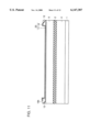
- FIG. 1 is a top plan view showing memory cells in an SRAM according to a first embodiment of the present invention.
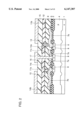
- FIG. 2 is a sectional view taken along the line II--II in FIG. 1.
- FIG. 3 is a top plan view showing the configuration of isolating insulating films and element formation regions in the SRAM according to the first embodiment.
- FIG. 4 is a top plan view showing the configuration of word lines and gate electrodes of driver transistors.
- FIG. 5 is a top plan view showing the storage node portion, Vcc interconnection portion and high-resistance portion of one memory cell.
- FIG. 6 is a top plan view showing the storage node portion, Vcc interconnection portion and high-resistance portion of another adjacent memory cell.
- FIG. 7 is a top plan view showing memory cells in an SRAM according to a second embodiment of the present invention.
- FIG. 8 is a sectional view taken along the line VIII--VIII in FIG. 7.
- FIG. 9 is a top plan view showing one storage node portion, Vcc interconnection portion, and high-resistance portion for each memory cell.
- FIG. 10 is a top plan view showing the other storage node portion, Vcc interconnection portion and high-resistance portion for each memory cell.
- FIG. 11 is a section view showing the configuration of a laser trimming fuse according to the second embodiment.
- FIG. 12 is an equivalent circuit diagram for illustrating the characteristics of the SRAM according to the second embodiment.
- FIG. 13 is a graph showing a relation between the heat treatment temperature and the carrier concentration.
- FIG. 14 is a graph showing a relation between the resistance value and the impurity concentration.
- FIG. 1 is a top plan view showing 2 ⁇ 4 memory cells in an SRAM according to the first embodiment of the present invention.
- FIG. 2 is a sectional view taken along the line II--II in FIG. 1.
- a p - type well region 4 is formed in an n - type silicon substrate 1.
- An n + impurity region 8 is formed on the surface of p - type well region 4.
- a field insulating film 2 is formed, selectively with a thickness of 200 to 500 nm.
- a gate insulating film 5 Formed on an element formation region, which is surrounded by field insulating film 2, is a gate insulating film 5, on which a gate electrode (a word line) 7a of an access transistor and a gate electrode 7b of a driver transistor are formed.
- An interlayer insulating film 9 is formed to cover word line 7a and gate electrode 7b. Interlayer insulating film 9 is provided with a contact hole 10. A storage node portion 11a is formed from within contact hole 10 to extend onto interlayer insulating film 9. A Vcc interconnection portion 11b and a high-resistance portion 11c are also formed on interlayer insulating film 9.
- a common conductive layer is patterned to form storage node portion 11a, Vcc interconnection portion 11b and high-resistance portion 11c, and an interlayer insulating film 12 is formed to cover them.
- a contact hole 13 is formed through interlayer insulating films 12, 9 to reach gate electrode 7b.
- a storage node portion 14a is formed from within contact hole 13 to extend onto interlayer insulating film 12.
- a Vcc interconnection portion 14b and a high-resistance portion 14c are formed on interlayer insulating film 12.
- Storage node portion 14a, Vcc interconnection portion 14b and high-resistance portion 14c are also formed by patterning a common conductive layer, and an interlayer insulating film 15 is formed to cover them. Through interlayer insulating films 15, 12, and 9, a contact hole 16 is formed to reach n + impurity region 8. A bit line 17 is formed from within contact hole 16 to extend onto interlayer insulating film 15.
- the above-mentioned field insulating film 2 is formed to define the element formation region 3.
- a p type impurity such as boron (B)
- boron (B) is implanted into the entire main surface of n - type silicon substrate 1 at 200 to 700 keV in an amount of the order of 1.0 ⁇ 10 12 to 1.0 ⁇ 10 13 cm -2 .
- the threshold voltage Vth of an access transistor and driver transistor is set by further implanting p type impurities, such as boron (B), for example at 30 to 70 keV in an amount of about 3.0 ⁇ 10 12 cm -2 .
- p - type well region 4 is formed with the impurity concentration of the order of 10 16 to 10 18 /cm 3 .
- n - type silicon substrate 1 is subjected to thermal oxidation to form gate insulating film 5 with a thickness of about 4 to about 10 nm.
- a contact hole 6 is formed to expose a prescribed region in element formation region 3.
- a first layer of polycrystalline silicon film is formed using LPCVD (Low Pressure Chemical Vapor Deposition), by mixing gases such as phosphine (PH 3 ).
- LPCVD Low Pressure Chemical Vapor Deposition
- This polycrystalline silicon film has a thickness of about 50 to about 200 nm, and includes phosphorus of the order of 1.0 to 8.0 ⁇ 10 20 cm -3 , which film is patterned to form word line 7a and gate electrode 7b as shown in FIG. 4.
- word line 7a and gate electrode 7b may be formed by a so-called polycide interconnection, which is made of a metal silicide film such as a tungsten silicide (WSi 2 ) and a phosphorus-doped polycrystalline film.
- the first layer of polycrystalline silicon film has sheet resistance of 10 to 100 ⁇ / ⁇ .
- n type impurities such as arsenic are implanted into element formation region 3 to form n + impurity region 8, and hence an access transistor and a driver transistor.
- Each memory cell in an SRAM has a pair of access transistors and a pair of driver transistors.
- a certain region in a semiconductor substrate where the pair of access transistors and the pair of driver transistors are formed is herein referred to as a unit region 18.
- unit region 18 has a shorter side with a length Lx in the direction of a word line and a longer side with a length Ly in the direction of a bit line. Note that, in some layout, unit region 18 may be in the form of a square.
- an interlayer insulating film 9 is formed to cover word line 7a and gate electrode 7b, which film has a thickness of about 100 to about 1000 nm, and in which a contact hole 10 is formed as shown in FIG. 5.
- LPCVD for example, is used to deposit a second layer of polycrystalline silicon film with a thickness of approximately 60 nm.
- This polycrystalline silicon film is patterned, and then phosphorus (P), for example, is implanted thereinto at 30 keV in an amount of the order of 1.0 ⁇ 10 13 cm -2 .
- a resist is formed to cover a portion at which high-resistance portion 11c is to be formed.
- arsenic (As) is implanted into the polycrystalline silicon film at 20 keV in an amount of 1.0 ⁇ 10 14 to 1.0 ⁇ 10 15 cm -2 .
- annealing is performed at a temperature of about 700° C. to about 800° C. for about 20 minutes.
- storage node portion 11a, Vcc interconnection portion 11b and high-resistance portion 11c are formed.
- high-resistance portion 11c which had been covered by the resist during the above-mentioned arsenic-implantation, only phosphorus has been implanted.
- the resistance value at high-resistance portion 11c is 100M to 10 T ⁇ each.
- Storage node portion 11a and Vcc interconnection portion 11b, both of which are low-resistance portions have a sheet resistance value of 1 k to 100 k ⁇ / ⁇ .
- the length L R of high-resistance portion 11b is made longer than the length Ly of the longest side of unit region 18. Therefore, even if the memory cell size is reduced, an adequate length of high-resistance portion 11c can be secured, ensuring a high resistance value. As a result, there can be obtained an SRAM reduced in power consumption.
- LPCVD is used to deposit on the entire surface a silicon oxide film with a thickness of about 100 to about 300 nm, to form an interlayer insulating film 12.
- a contact hole 13 is formed through interlayer insulating films 12, 9 to reach gate electrode 7b.
- a third layer of polycrystalline silicon film is deposited to have a thickness of about 100 nm. This polycrystalline silicon film is patterned to form storage node portion 14a, Vcc interconnection portion 14b and high-resistance portion 14c as shown in FIG. 6.
- arsenic is implanted into the above-mentioned polycrystalline silicon film at 30 keV in an amount of about 2.2 ⁇ 10 13 cm -2 .
- arsenic is implanted into the polycrystalline silicon film at 20 keV in an amount of 1.0 ⁇ 10 14 to 1.0 ⁇ 10 15 cm -2 .
- the impurities are then activated under the same condition as in the second layer of polycrystalline silicon film, and thus storage node portion 14a and Vcc interconnection portion 14b, both with low resistance, are provided.
- high-resistance portion 14c In high-resistance portion 14c, only 2.2 ⁇ 10 13 cm -2 of arsenic has been implanted, since it had been covered by a resist during the second arsenic-implantation. As a result, high-resistance portion 14c has a resistance value of 100M to 10 T ⁇ each, which is higher than the sheet resistance of 1 k to 100 k ⁇ / ⁇ at storage node portion 14a and Vcc interconnection portion 14b.
- impurities implanted into high-resistance portions 11c and 14c are made different from each other both in amount and in type, and the two portions also have different thickness, which is due to the following reasons.
- the high resistance values at high-resistance portions 11c, 14c cannot be made equal when they are made to have equal thickness and same impurity-implantation condition, since high-resistance portion 11c is subjected to extra heat treatment for a time period from the moment high-resistance portion 11c has been formed until the high-resistance portion 14c is complete, and also each of high-resistance portions 11c, 14c has underlayers uneven in thickness. More specifically, if high-resistance portions 11c, 14c are formed with same film thickness, same impurities, and same implantation condition, generally, high-resistance portion 11c, which is located lower in layers than high-resistance portion 14c, represents lower resistance. That is, as shown in FIG.
- the carrier concentration in each portion varies according to changes in temperature and time for heat treatment after its formation, and so does the resistance value therein, which is proportional to the carrier concentration.
- the resistance value also varies depending on the impurity elements to be used.
- FIGS. 13 and 14 have been disclosed in "Polycrystalline Silicon for Integrated Circuit Applications" from KLUWER ACADEMIC PUBLISHERS.
- high-resistance portion 14c when using different impurities, it is required to increase the dose being used to form high-resistance portion 14c in the range of 10% to 250%, or, to make its film thickness 10% to 100% greater.
- the ultimate resistance values at high-resistance portions 11c and 14c can be made approximately equal, and thus it becomes possible to reduce the variation in characteristics between memory cells.
- interlayer insulating film 15 of about 300 to about 1000 nm thick
- contact hole 16 a contact hole 16
- bit line 17 made of, for example, 100 to 500 nm thick aluminum.
- a memory cell in the SRAM is provided with a pair of access transistors A1, A2, a pair of driver transistors D1, D2, and a pair of load elements R1, R2.
- BIT and /BIT in FIG. 12 represent bit lines.
- Such capacitance increases the storage capacity of the storage nodes of a memory cell, thereby making it possible to improve immunity to a soft error.
- load elements R1 and R2 in each memory cell are formed by different conductive layers.
- high-resistance portions 11c and 14c are formed by separate interconnections layers.
- an overlapping portion is provided between storage node portion 11a and storage node portion 14a or high-resistance portion 14c, or, between storage node portion 14a and storage node portion 11a or high-resistance portion 11c, to form capacitance. Accordingly, the storage capacitance Q for the storage nodes can be increased.
- the interlayer insulating film 12 shown in FIG. 8 by a silicon oxide film (SiO 2 ) with a thickness of about 5 to about 100 nm, or, a high-dielectric film having a dielectric constant higher than that of a silicon oxide film, such as a silicon nitride film (Si 3 N 4 ), Si 3 N 4 /SiO 2 or SiO 2 /Si 3 N 4 /SiO 2 , to increase capacitance.
- a silicon oxide film SiO 2
- Si 3 N 4 silicon nitride film
- Vcc interconnection portions 11b and 14b are shunted to each other through contact hole 19a. Accordingly, those Vcc interconnection portions can be formed by a conductive layer having a double-layered structure, and thus the resistance values at the Vcc interconnections can be reduced.
- a contact hole 19b having a large opening diameter may be first formed, and then, a polycrystalline silicon film 11 for forming Vcc interconnection portion 11b and another polycrystalline silicon film 14 for Vcc interconnection portion 14b may be formed thereon.
- a laser trimming fuse 20 can be formed by those two polycrystalline silicon films. Propagation delay in a fuse circuit can thus be suppressed using such a fuse 20.
- a static random access memory according to the present invention permits reduction in power consumption as well as improvement in immunity to soft errors. Therefore, a high-performance, high-reliability static random access memory can be realized.
Abstract
Description
Claims (9)
Applications Claiming Priority (2)
| Application Number | Priority Date | Filing Date | Title |
|---|---|---|---|
| JP10020828A JPH11220040A (en) | 1998-02-02 | 1998-02-02 | Static semiconductor memory device |
| JP10-020828 | 1998-02-02 |
Publications (1)
| Publication Number | Publication Date |
|---|---|
| US6147387A true US6147387A (en) | 2000-11-14 |
Family
ID=12037914
Family Applications (1)
| Application Number | Title | Priority Date | Filing Date |
|---|---|---|---|
| US09/116,889 Expired - Fee Related US6147387A (en) | 1998-02-02 | 1998-07-16 | Static random access memory |
Country Status (2)
| Country | Link |
|---|---|
| US (1) | US6147387A (en) |
| JP (1) | JPH11220040A (en) |
Citations (7)
| Publication number | Priority date | Publication date | Assignee | Title |
|---|---|---|---|---|
| US3570114A (en) * | 1968-01-29 | 1971-03-16 | Texas Instruments Inc | Bi-layer insulation structure including polycrystalline semiconductor material for integrated circuit isolation |
| JPS60138956A (en) * | 1983-12-27 | 1985-07-23 | Toshiba Corp | Semiconductor memory device |
| JPS61185964A (en) * | 1985-02-13 | 1986-08-19 | Toshiba Corp | Semiconductor memory |
| JPS61283161A (en) * | 1985-06-10 | 1986-12-13 | Hitachi Ltd | Semiconductor device |
| JPS6380566A (en) * | 1986-09-24 | 1988-04-11 | Nec Corp | Static semiconductor memory |
| JPH03165560A (en) * | 1989-11-24 | 1991-07-17 | Sony Corp | Semiconductor memory |
| US6013940A (en) * | 1994-08-19 | 2000-01-11 | Seiko Instruments Inc. | Poly-crystalline silicon film ladder resistor |
-
1998
- 1998-02-02 JP JP10020828A patent/JPH11220040A/en active Pending
- 1998-07-16 US US09/116,889 patent/US6147387A/en not_active Expired - Fee Related
Patent Citations (7)
| Publication number | Priority date | Publication date | Assignee | Title |
|---|---|---|---|---|
| US3570114A (en) * | 1968-01-29 | 1971-03-16 | Texas Instruments Inc | Bi-layer insulation structure including polycrystalline semiconductor material for integrated circuit isolation |
| JPS60138956A (en) * | 1983-12-27 | 1985-07-23 | Toshiba Corp | Semiconductor memory device |
| JPS61185964A (en) * | 1985-02-13 | 1986-08-19 | Toshiba Corp | Semiconductor memory |
| JPS61283161A (en) * | 1985-06-10 | 1986-12-13 | Hitachi Ltd | Semiconductor device |
| JPS6380566A (en) * | 1986-09-24 | 1988-04-11 | Nec Corp | Static semiconductor memory |
| JPH03165560A (en) * | 1989-11-24 | 1991-07-17 | Sony Corp | Semiconductor memory |
| US6013940A (en) * | 1994-08-19 | 2000-01-11 | Seiko Instruments Inc. | Poly-crystalline silicon film ladder resistor |
Also Published As
| Publication number | Publication date |
|---|---|
| JPH11220040A (en) | 1999-08-10 |
Similar Documents
| Publication | Publication Date | Title |
|---|---|---|
| US5536674A (en) | Process for forming a static-random-access memory cell | |
| KR100544943B1 (en) | Semiconductor integrated circuit device and process for manufacturing the same | |
| US5700705A (en) | Semiconductor integrated circuit device | |
| US4984200A (en) | Semiconductor circuit device having a plurality of SRAM type memory cell arrangement | |
| US5744384A (en) | Semiconductor structures which incorporate thin film transistors | |
| US5521860A (en) | CMOS static memory | |
| US6512245B2 (en) | Semiconductor integrated circuit device | |
| US4803534A (en) | Semiconductor device sram to prevent out-diffusion | |
| US5920097A (en) | Compact, dual-transistor integrated circuit | |
| JP2998679B2 (en) | Semiconductor memory device and method of manufacturing the same | |
| US5497022A (en) | Semiconductor device and a method of manufacturing thereof | |
| US6303422B1 (en) | Semiconductor memory and manufacturing method thereof | |
| JPH03154377A (en) | Compact static ram holding polycrystal silicon diode load | |
| US5200356A (en) | Method of forming a static random access memory device | |
| US5990528A (en) | Thin film transistor with titanium nitride or refractory metal gate in SRAM device serving as source/drain contact electrode of an independent FET | |
| US5610856A (en) | Semiconductor integrated circuit device | |
| KR100394126B1 (en) | Semiconductor device and method of manufacturing the same | |
| JP3712313B2 (en) | SRAM cell structure and manufacturing method thereof | |
| US6147387A (en) | Static random access memory | |
| EP0339586B1 (en) | Semiconductor device having improved gate capacitance and manufacturing method therefor | |
| JPH098244A (en) | Semiconductor device and its manufacture | |
| US20070181958A1 (en) | Semiconductor device and method of forming the same | |
| US6350645B1 (en) | Strapping via for interconnecting integrated circuit structures | |
| US5731618A (en) | Semiconductor device and method of manufacturing thereof | |
| JPH06188388A (en) | Semiconductor memory device |
Legal Events
| Date | Code | Title | Description |
|---|---|---|---|
| AS | Assignment |
Owner name: MITSUBISHI DENKI KABUSHIKI KAISHA, JAPAN Free format text: ASSIGNMENT OF ASSIGNORS INTEREST;ASSIGNOR:ISHIGAKI, YOSHIYUKI;REEL/FRAME:009329/0622 Effective date: 19980604 |
|
| FEPP | Fee payment procedure |
Free format text: PAYOR NUMBER ASSIGNED (ORIGINAL EVENT CODE: ASPN); ENTITY STATUS OF PATENT OWNER: LARGE ENTITY |
|
| FPAY | Fee payment |
Year of fee payment: 4 |
|
| FPAY | Fee payment |
Year of fee payment: 8 |
|
| AS | Assignment |
Owner name: RENESAS ELECTRONICS CORPORATION, JAPAN Free format text: ASSIGNMENT OF ASSIGNORS INTEREST;ASSIGNOR:MITSUBISHI DENKI KABUSHIKI KAISHA;REEL/FRAME:025980/0219 Effective date: 20110307 |
|
| REMI | Maintenance fee reminder mailed | ||
| LAPS | Lapse for failure to pay maintenance fees | ||
| STCH | Information on status: patent discontinuation |
Free format text: PATENT EXPIRED DUE TO NONPAYMENT OF MAINTENANCE FEES UNDER 37 CFR 1.362 |
|
| FP | Lapsed due to failure to pay maintenance fee |
Effective date: 20121114 |