US6140678A - Trench-gated power MOSFET with protective diode - Google Patents
Trench-gated power MOSFET with protective diode Download PDFInfo
- Publication number
- US6140678A US6140678A US08/962,867 US96286797A US6140678A US 6140678 A US6140678 A US 6140678A US 96286797 A US96286797 A US 96286797A US 6140678 A US6140678 A US 6140678A
- Authority
- US
- United States
- Prior art keywords
- mosfet
- cells
- diode
- trench
- region
- Prior art date
- Legal status (The legal status is an assumption and is not a legal conclusion. Google has not performed a legal analysis and makes no representation as to the accuracy of the status listed.)
- Expired - Lifetime
Links
Images


Classifications
-
- H—ELECTRICITY
- H10—SEMICONDUCTOR DEVICES; ELECTRIC SOLID-STATE DEVICES NOT OTHERWISE PROVIDED FOR
- H10D—INORGANIC ELECTRIC SEMICONDUCTOR DEVICES
- H10D30/00—Field-effect transistors [FET]
- H10D30/60—Insulated-gate field-effect transistors [IGFET]
- H10D30/64—Double-diffused metal-oxide semiconductor [DMOS] FETs
- H10D30/66—Vertical DMOS [VDMOS] FETs
- H10D30/668—Vertical DMOS [VDMOS] FETs having trench gate electrodes, e.g. UMOS transistors
-
- H—ELECTRICITY
- H10—SEMICONDUCTOR DEVICES; ELECTRIC SOLID-STATE DEVICES NOT OTHERWISE PROVIDED FOR
- H10D—INORGANIC ELECTRIC SEMICONDUCTOR DEVICES
- H10D30/00—Field-effect transistors [FET]
- H10D30/60—Insulated-gate field-effect transistors [IGFET]
- H10D30/63—Vertical IGFETs
-
- H—ELECTRICITY
- H10—SEMICONDUCTOR DEVICES; ELECTRIC SOLID-STATE DEVICES NOT OTHERWISE PROVIDED FOR
- H10D—INORGANIC ELECTRIC SEMICONDUCTOR DEVICES
- H10D62/00—Semiconductor bodies, or regions thereof, of devices having potential barriers
- H10D62/10—Shapes, relative sizes or dispositions of the regions of the semiconductor bodies; Shapes of the semiconductor bodies
- H10D62/17—Semiconductor regions connected to electrodes not carrying current to be rectified, amplified or switched, e.g. channel regions
- H10D62/393—Body regions of DMOS transistors or IGBTs
-
- H—ELECTRICITY
- H10—SEMICONDUCTOR DEVICES; ELECTRIC SOLID-STATE DEVICES NOT OTHERWISE PROVIDED FOR
- H10D—INORGANIC ELECTRIC SEMICONDUCTOR DEVICES
- H10D84/00—Integrated devices formed in or on semiconductor substrates that comprise only semiconducting layers, e.g. on Si wafers or on GaAs-on-Si wafers
- H10D84/101—Integrated devices comprising main components and built-in components, e.g. IGBT having built-in freewheel diode
- H10D84/141—VDMOS having built-in components
- H10D84/148—VDMOS having built-in components the built-in components being breakdown diodes, e.g. Zener diodes
-
- H—ELECTRICITY
- H10—SEMICONDUCTOR DEVICES; ELECTRIC SOLID-STATE DEVICES NOT OTHERWISE PROVIDED FOR
- H10D—INORGANIC ELECTRIC SEMICONDUCTOR DEVICES
- H10D89/00—Aspects of integrated devices not covered by groups H10D84/00 - H10D88/00
- H10D89/60—Integrated devices comprising arrangements for electrical or thermal protection, e.g. protection circuits against electrostatic discharge [ESD]
- H10D89/601—Integrated devices comprising arrangements for electrical or thermal protection, e.g. protection circuits against electrostatic discharge [ESD] for devices having insulated gate electrodes, e.g. for IGFETs or IGBTs
- H10D89/611—Integrated devices comprising arrangements for electrical or thermal protection, e.g. protection circuits against electrostatic discharge [ESD] for devices having insulated gate electrodes, e.g. for IGFETs or IGBTs using diodes as protective elements
-
- H—ELECTRICITY
- H10—SEMICONDUCTOR DEVICES; ELECTRIC SOLID-STATE DEVICES NOT OTHERWISE PROVIDED FOR
- H10D—INORGANIC ELECTRIC SEMICONDUCTOR DEVICES
- H10D62/00—Semiconductor bodies, or regions thereof, of devices having potential barriers
- H10D62/10—Shapes, relative sizes or dispositions of the regions of the semiconductor bodies; Shapes of the semiconductor bodies
- H10D62/124—Shapes, relative sizes or dispositions of the regions of semiconductor bodies or of junctions between the regions
- H10D62/126—Top-view geometrical layouts of the regions or the junctions
- H10D62/127—Top-view geometrical layouts of the regions or the junctions of cellular field-effect devices, e.g. multicellular DMOS transistors or IGBTs
Definitions
- This invention relates to power field-effect transistors and, in particular, to a metal-oxide-silicon field-effect transistor (MOSFET) in which the gate is positioned in a trench formed on the surface of the silicon.
- MOSFET metal-oxide-silicon field-effect transistor
- Trench-gated MOSFETs are a class of MOSFETs in which the gate is positioned in a trench that is formed at the surface and extends into the silicon.
- the gate is formed in lattice-like geometric pattern which defines individual cells of the MOSFET, the pattern normally taking the form of closed polygons (squares, hexagons, etc.) or a series of interdigitated stripes or rectangles.
- the current flows in vertical channels which are formed adjacent to the sides of the trenches.
- the trenches are filled with a conductive gate material, typically doped polysilicon, which is insulated from the silicon by a dielectric layer normally consisting of silicon dioxide.
- a power MOSFET Two critical characteristics of a power MOSFET are its breakdown voltage, i.e., the voltage at which it begins to conduct current when in an off condition, and its on-resistance, i.e., its resistance to current flow when in an on condition.
- the on-resistance of a MOSFET generally varies directly with its cell density, since when there are more cells per unit area there is also a greater total "gate width" (around the perimeter of each cell) for the current to pass through.
- the breakdown voltage of a MOSFET depends primarily on the doping concentrations and locations of the source, body and drain regions in each MOSFET cell.
- the MOSFET is typically formed in a lightly-doped epitaxial layer of silicon which is grown on a heavily-doped silicon substrate.
- the gate trenches normally extend into the epitaxial layer and are frequently rectangular, with flat bottoms bounded by corners. This configuration creates a problem in that, when the MOSFET is turned off, the electric field reaches a maximum near the corners of the gate trenches. This can lead to avalanche breakdown and impact ionization near the surface of the gate oxide, with the consequent generation of carriers. If the carriers are generated within a mean free path of the interface between the silicon and the gate oxide, they may have sufficient energy to pass through the interface and become injected into the gate oxide layer.
- Hot carrier injection can ultimately damage the gate oxide layer, causing changes in threshold voltage, transconductance or on-resistance, and thereby impair or destroy the MOSFET.
- U.S. Pat. No. 5,072,266 teaches a technique of suppressing voltage breakdown near the gate by the formation, in the MOSFET cell, of a deep central body diffusion that extends below the bottom of the trenches. This deep central diffusion shapes the electric field in such a way that breakdown occurs in the bulk silicon away from the gate, in a location which prevents hot carriers from reaching the gate oxide layer.
- FIG. 1 A cross-sectional view of a MOSFET in accordance with U.S. Pat. No. 5,072,266 is shown in FIG. 1, which illustrates a MOSFET cell 10 containing a trenched gate 11, an N+ source region 12, an N+ substrate (drain) 13, an N-epitaxial layer 14, and a deep central P+ diffusion 15. Note that the lowest point of P+ diffusion 15 is below the bottom of gate 11.
- the doping of deep P+ diffusion 15 is greater than the doping of P-body 16 in the region of the channel, designated by the dashed line and reference numeral 17.
- the distance Y S between the gate trenches must be maintained at or above a minimum value. Otherwise, the deep P+ dopant will diffuse into the channel 17 and raise the threshold voltage V tn of the device.
- the value of Y S along with the thickness of the gate, defines the cell density and helps to determine the on-resistance of the MOSFET.
- FIGS. 15A and 15B show simulations of the current flow lines in a conventional MOSFET having a flat bottomed P-body region and a MOSFET having a deep P+ diffusion, respectively.
- the current lines in FIG. 15B are limited to a spreading angle (an analytical approximation used to describe the epitaxial current uniformity) of about 45 to 47 degrees (measured at the 95% flow lines), resulting in sub-optimum utilization of the N-epitaxial region and a higher specific on-resistance than in the device portrayed in FIG. 15A.
- ⁇ is the current spreading angle
- Y CELL is the total width of the MOSFET cell
- Y G is the distance between the gate trenches.
- MOSFET complementary metal-oxide-semiconductor
- the dimensions of the device are generally scaled down.
- the cell density is increased and the epitaxial layer is made thinner, even to the point that the gate trenches may extend into the heavily-doped substrate.
- MOSFET 20 in FIG. 2A Such a MOSFET is illustrated as MOSFET 20 in FIG. 2A.
- Diode D DB represents the PN junction between N-epitaxial layer 14 and P-body region 22, and capacitor C GD represents the capacitor across the gate oxide layer 21A.
- the trench-gated MOSFET of this invention is formed in a semiconductor chip which includes a substrate alone or in combination with an overlying epitaxial layer.
- the gate of the MOSFET is formed in a trench which extends downward from the surface of the chip.
- the MOSFET includes a source region of a first conductivity type, a body region of a second conductivity type, and a drain region of the first conductivity type, which are arranged vertically along a side wall of the trench.
- the gate trenches may extend into the epitaxial layer, or through the epitaxial layer into the substrate.
- the MOSFET is formed as a plurality of cells which are defined by the gate trench.
- the cells may be of any shape.
- the cells may be in the form of a square or hexagon or a series of parallel stripes or rectangles.
- a protective diffusion of the second conductivity type which forms a PN junction with first conductivity material in the epitaxial layer or substrate.
- This PN junction functions as a diode.
- a metal layer ties the protective diffusion (i.e., one terminal of the diode) to the source regions of the MOSFET cells such that the diode is connected in parallel with the channels of the MOSFET cells.
- the protective diffusion is formed in certain of the cells in a selected pattern across the MOSFET.
- the protective diffusion of second conductivity type operates to reduce the strength of the electric field across the gate oxide and at the corners of the trenches and limits the formation of hot carriers in the vicinity of the trench, particularly in embodiments wherein the trenches extend into the epitaxial layer.
- Avalanche breakdown may be induced by any number of mechanisms (reachthrough, radius of curvature, etc.) so long as the avalanching region is spatially separated from the gate trench.
- the diode can also operate as a voltage clamp and thereby limit the voltage across the gate oxide layer, particularly in embodiments wherein the trenches extend into the substrate and the gate oxide must support the entire voltage drop across the MOSFET.
- one cell containing a protective diffusion is provided for a selected number of active MOSFET cells (“active cells”), in a repetitive pattern across the MOSFET.
- active cells active MOSFET cells
- the number of diode cells per active cells is determined by the design criteria of the MOSFET. In general, for example, MOSFETs which are expected to experience breakdown more often will require a greater proportion of diode cells.
- the presence of the diode cell also tends to carry a large portion of the drain-to-body diode current when the MOSFET is operated with its body diode forward-conducting.
- Such operation commonly occurs when an inductor or motor is driven by a push-pull or bridge-configured pair of MOSFETs.
- High diode currents in the active cells are undesirable since they may lead to minority charge storage, which complicates diode turn-off (forced diode reverse recovery) and may lead to snapback of the parasitic source-body-drain active cell NPN bipolar transistor when a high reverse voltage is once again applied across the device.
- FIG. 1 illustrates a cross-sectional view of a conventional trench-gated MOSFET containing a deep central diffusion to reduce the electric field at the corners of the trenches.
- FIG. 2A illustrates a cross-sectional view of a conventional trench-gated MOSFET without a deep central diffusion and wherein the trenches extend into the substrate.
- FIG. 2B illustrates an equivalent circuit diagram for the MOSFET of FIG. 2A.
- FIG. 3 illustrates a cross-sectional view of a first embodiment of this invention including a protective diffusion in an adjacent MOSFET cell.
- FIG. 4A illustrates a cross-sectional view of a second embodiment of this invention including a protective diffusion in an adjacent MOSFET cell and wherein the trenches extend into the substrate.
- FIG. 4B illustrates an equivalent circuit diagram for the MOSFET of FIG. 4A.
- FIG. 5 illustrates a top view of a conventional MOSFET cell.
- FIG. 6 illustrates a top view of a square-celled MOSFET in accordance with this invention.
- FIG. 7 illustrates a detailed top view of the square-celled MOSFET of FIG. 6.
- FIG. 8 illustrates a top view of a striped-cell MOSFET in accordance with this invention.
- FIG. 9 illustrates another cross-sectional view of the second embodiment in accordance with this invention.
- FIG. 10 illustrates a cross-sectional view of a third embodiment in accordance with this invention.
- FIG. 11 illustrates a cross-sectional view of a fourth embodiment in accordance with this invention.
- FIG. 12 illustrates a cross-sectional view of a fifth embodiment in accordance with this invention.
- FIGS. 13A and 13B illustrate cross-sectional and top views, respectively, of a sixth embodiment, which includes a wide protective cell.
- FIGS. 14A-14E illustrate the steps of a process of fabricating the MOSFET shown in FIG. 3.
- FIGS. 15A and 15B illustrate simulations of the current flow lines in a MOSFET having a flat-bottomed body region and a MOSFET having a deep central body diffusion as taught in U.S. Pat. No. 5,072,266, respectively.
- FIG. 16 illustrates a view of a MOSFET which shows the geometrical relationship between the current-spreading angel and the depth within the epitaxial layer at which uniform conduction is achieved.
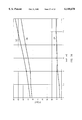
- FIG. 17 illustrates a graph showing specific on-resistance as a function of cell density in a MOSFET having a deep central diffusion and in a MOSFET having distributed diode cells.
- FIG. 18 illustrates a graph showing the variation of specific on-resistance as a function of gate bias for MOSFETs having a cell density of 12 Mcells/in 2 and 32 Mcells/in 2 , respectively.
- FIGS. 19A and 19B illustrate simulations of the current flow lines in a MOSFET operating in its linear region during normal conduction and in a MOSFET having a diode cell and experiencing avalanche breakdown.
- FIG. 20 illustrates a graph showing the unclamped inductive switching current and drain voltage in a MOSFET.
- FIG. 21 illustrates a graph showing the measured I-V and breakdown characteristics of a MOSFET.
- FIG. 22 illustrates a graph showing the on-resistance of various components of a packaged MOSFET as a function of gate bias.
- FIGS. 23A and 23B illustrate simulations showing the location of avalanche breakdown in flat-bottomed MOSFETs having relatively thick and relatively thin gate oxide layers, respectively.
- FIG. 24 illustrates a graph showing the breakdown voltage as a function normalized gate oxide thickness for a MOSFET having a deep central body diffusion, a MOSFET having a flat-bottomed body region, and a MOSFET having distributed diode cells in accordance with this invention.
- FIG. 25 illustrates a graph showing the I-V characteristic of a MOSFET.
- FIG. 26 illustrates a graph showing specific on-resistance as a function of gate bias for thin (12-V gate rated) and thick (20-V gate rated) oxide MOSFETs having cell densities of 12 Mcells/in 2 and 32 Mcells/in 2 .
- FIG. 27 illustrates a cross-sectional view of a "reachthrough" type of MOSFET structure, including a MOSFET cell and a diode cell.
- FIG. 28 illustrates a graph showing the breakdown voltage as a function of the epitaxial layer thickness 20-V drain, 12-V gate, N-channel MOSFET using the "reachthrough” approach.
- FIG. 29 illustrates a graph showing the breakdown voltage as a function of the epitaxial layer thickness 30-V drain, 20-V gate, N-channel MOSFET using the "reachthrough” approach.
- FIG. 30 illustrates a cross-sectional view of a "stepped epi" type of MOSFET structure, including a MOSFET cell and a diode cell.
- FIG. 31 illustrates a graph showing the breakdown voltage as a function of the dopant concentration of the lower epi sublayer in 20-V drain, 12-V gate N-channel device which uses the "stepped epi" approach.
- FIG. 32 illustrates a graph of the breakdown voltage in the diode cell (horizontal axis) as a function of the resistivity and dopant concentration of the lower epi sublayer.
- FIGS. 33, 34 and 35 show various data for a 30-V drain, 20-V gate N-channel device which uses the stepped epi approach.
- FIG. 36 shows various data for a 30-V drain, 20-V gate P-channel device which uses the reachthrough approach.
- FIGS. 37 and 38 show the breakdown voltage of the diode cell and the difference between the breakdown voltages for the diode and MOSFET cells as a function of epi concentration for different implant doses and drive-in times for the diode diffusion.
- FIG. 39 shows the breakdown voltage for an N-type diode diffusion as a function of the thickness of the P-epi layer for six different implant doses.
- FIG. 40 shows the breakdown voltage for an N-type diode diffusion as a function of the implant dose for seven different thicknesses of the P-epi layer.
- a first embodiment of the invention is illustrated in FIG. 3.
- a trench-gated MOSFET 30 is formed in N-epitaxial layer 14, which is grown on the top surface of N+ substrate 13.
- a gate 31, formed in a trench 32, is separated from the semiconductor material by an oxide layer 31A.
- a cell 35 of MOSFET 30 also includes a P-body region 33, a shallow P+ contact region 33A, and an N+ source region 34.
- a metal layer 36 makes contact with and forms a short between P-body region 33 and N+ source region 34.
- N+ substrate 13 serves as the drain of MOSFET 30 and may be contacted from the bottom.
- a submerged N+ layer instead of the N+ substrate could be used as the drain, and the drain could be contacted from the top side of the structure by means of, for example, an N+ sinker region and a top side contact.
- PN junction 39 represents a diode which is connected in parallel with the channel of cell 35.
- Protective diffusion 38 limits the strength of the electric field and resulting carrier formation near the corners of trench 32 and thereby eliminates the need for a deep central diffusion in MOSFET cell 35.
- the dimensions of MOSFET cell 35 may be substantially reduced and the cell density of MOSFET 30 may be significantly increased.
- the width of each side of N+ source region 34 may be reduced to about 1.0 ⁇ m
- the width of the contact between metal layer 36 and the P+ contact region for P-body 33 may be reduced to about 1.0 ⁇ m, so that the total width between trenches 32 may be on the order of 3.5 ⁇ m, although in practice the total width between trenches 32 might be set at 5.0 ⁇ m. This compares with a minimum width of about 8.0 ⁇ m for a MOSFET cell which contains a deep central diffusion (see FIG. 1).
- FIG. 4A illustrates a MOSFET 40 which includes a MOSFET cell 41 similar to the cell shown in FIG. 2A. That is, trenches 43 extend through the N-epitaxial layer 14 and into the N+ substrate 13, and cell 41 does not include a central deep P+ diffusion. In an adjacent cell 42, a protective P+ diffusion 44 is formed, with the lower junction of diffusion 44 reaching the top surface of N+ substrate 13.
- FIG. 4B illustrates an equivalent circuit for MOSFET 40. Since the corners of trench 43 are located in the N+ substrate 13, which being heavily-doped cannot support a strong electric field, the problem of the electric field at the corners of the trenches is largely eliminated. Instead, the critical factor becomes the strength of the electric field between the gate 45 and the N+ substrate 13, i.e., across the gate oxide layer 45A. This location is represented by a capacitor C GD in FIG. 4B.
- the PN junction between P-body region 22 and N-epitaxial layer 14 is represented by a diode D DB
- the PN junction between P+ diffusion 44 and N+ substrate 13 is represented by a diode D P+/N+ . As shown, both diode D DB and diode D P+/N+ are connected in parallel with the channel of MOSFET cell 41.
- FIG. 5 shows a top view of the conventional MOSFET 10 shown in FIG. 1.
- the protective deep P+ region 15 is shown at the center of each square cell, surrounded by the N+ source region 12 and the gate 11. Four complete cells are shown in FIG. 5.
- FIG. 6 shows a top view of the MOSFET 30 shown in FIG. 3.
- a top view of MOSFET 40 shown in FIG. 4A would appear similar. Because the protective P+ region at the center of each cell has been eliminated, the dimensions of the cells have been reduced.
- the cells which contain the P+ diffusions (sometimes referred to as "diode cells") are also shown. In FIG. 6, there is one diode cell for every eight active MOSFET cells (total of nine cells).
- FIG. 7 shows a detailed top view of three of the cells shown in FIG. 6 (two active MOSFET cells and one diode cell).
- Y S represents the distance between the trenched gates and Y G represents the cross-sectional width of the trench (not to be confused with the gate width W).
- n-1 of these cells are active MOSFET cells, the total gate width W in the n cells is equal to:
- the area-to-width ratio A/W (a figure of merit indicating how effectively a gate width W is packed into an area A) equals:
- n/(n-1) the ratio of A/W for a MOSFET which contains diode cells is increased by the factor n/(n-1), as compared with a conventional MOSFET with no diode cells.
- This "penalty" factor which arises from the fact that the diode cells carry no current, approaches unity as n increases.
- the penalty is counterbalanced by the increased total gate width (and hence current-carrying capacity) which is obtained by increasing the cell density of the device.
- n is determined by the frequency with which the MOSFET is expected to break down. Devices which are expected to break down more frequently will generally require a lower n, i.e., there must be a greater number of diode cells relative to the total number of cells.
- FIG. 17 illustrates a graph showing specific on-resistance (R DS A) as a function of cell density in a MOSFET having a deep P+ diffusion (curve 170) and a MOSFET having distributed diode cells (curve 172).
- R DS A specific on-resistance
- the specific on-resistance of the MOSFET containing deep P+ diffusions reaches a minimum after which it begins to increase as a result of current crowding and an increase in threshold voltage due to intrusion of the P+ body dopant into the channel.
- FIG. 18 shows the variation of the specific R DS A as a function of gate bias for the two devices. For devices with a 20-V gate rating, the threshold voltage was maintained at 2.9 V consistent with rated operation at 10- and 4.5-V gate biases.
- FIG. 19A illustrates the current flow lines of the device operating in its linear region during normal conduction before switching
- FIG. 19B illustrates the current flow lines after the device has been inductively switched.
- avalanche breakdown occurs in the diode cell, which conducts all of the current, without appreciable impact ionization, preavalanche or high gate oxide fields in the "off" active MOSFET cells.
- FIG. 20 shows that the measured UIS currents exceeded seven times the MOSFET's rated operating current, reaching current densities of over 950 A/cm 2 .
- the resulting die resistance of less than 2.0 m ⁇ is the lowest ever reported to our knowledge.
- On-resistance simulations and measurements on smaller die suggest that spreading resistance in the MOSFET's top metal may account for an additional resistance of as much as 0.5 m ⁇ .
- the packaging typically accounts for 33% of the packaged product's total resistance.
- the 32 Mcell/cm 2 MOSFET has the lowest specific on-resistance of any 30-V power MOSFET ever fabricated to our knowledge, and it is not subject to the UIS, reliability and area-scaling limitations of other similar devices.
- the gate oxide layer In order to optimize a MOSFET for low-voltage operation, however, the gate oxide layer must be down-scaled (i.e., thinned) both to achieve a low threshold voltage (without channel punchthrough) and to achieve a high channel transconductance.
- FPI field plate induced
- the breakdown voltage of the "1-of-N" diodes is set substantially below the voltage at which FPI breakdown occurs (FIG. 24).
- a P-channel MOSFET was fabricated in accordance with the "1-of-N" principles described herein.
- the drain of the MOSFET was designed, in accordance with known techniques, for operation at 20 V.
- the cell density was set at 32 Mcells/in 2
- the threshold voltage was set at 1.3 V.
- a die for a 10-A rated SO-8 sized package conducting over 50 A with a gate bias of only 2.5 V was used.
- FIG. 25 shows the I-V characteristics of the device.
- the measure specific on-resistance was 850 ⁇ -cm 2 at a gate bias of 2.5 V and 750 ⁇ -cm 2 at a gate bias of 2.7 V.
- the regularly distributed inclusion of non-active deep P+ cells in a vertical trench FET provides a voltage clamping feature which limits the carrier generation rate and electric field at the corners or in the vicinity of the trench gate.
- the reliability and survivability of the device in the presence of electrical overstressing is thereby improved without limiting on-resistance or cell density.
- the deep P+ region need not extend to the trench edge but may be made smaller than its cell geometry if desired.
- the deep P+ region need not extend below the trench if the trench overlaps the N+ substrate, in which case a PIN diode may be formed between the deep P+ region and the N+ substrate (see FIG. 11).
- a graph showing the breakdown voltage of a PIN diode (such as diode D2 in FIG.
- MOSFET cell dimensions can be significantly reduced, thereby increasing the cell density from 12 Mcell/in 2 to 32 Mcell/in 2 (5 Mcell/cm 2 ) without sacrificing the area or quality of the body contact.
- the parameter "n” can be varied from 2 (every other cell) to a large number such as 64 or more.
- the ability of the MOSFET to withstand avalanche breakdown can thus be controlled by design, with a penalty in on-resistance compared to a purely flat-bottom cell represented by the factor n/n-1. In many instances, this penalty factor can be adjusted to within a few percent of the ideal flat-bottom device.
- FIG. 8 illustrates a top view of an alternative MOSFET in which the cells are in the form of stripes.
- MOSFET 80 cells 81, 82, 83 and 84 are active MOSFET cells, and cell 85 is a diode cell which contains a protective P+ diffusion 86.
- Each of cells 81-84 contains a P+ contact region 87 and an N+ source region 88.
- Contact holes 89 two of which are shown in FIG. 8, are used to provide contact between a metal layer (not shown) and P+ region 87 and N+ source region 88 in MOSFET cells 81-84 and P+ region 86 in diode cell 85.
- Contact holes 89 may be arranged in a variety of patterns over cells 81-85.
- a contact hole 90 for making contact with gate 91 is also shown.
- P+ diode cell Another use of the P+ diode cell is to clamp the drain voltage so as to protect the gate oxide layer from overstress due to excessive electric fields between the gate and the N+ substrate. This situation arises particularly in embodiments where the trench gate extends into the substrate and the gate oxide layer at the bottom of the trench is therefore exposed to the entire voltage difference between the gate and substrate. Silicon dioxide is capable of withstanding a voltage equal to about 8 MV/cm. Using a safety factor of 50%, the industry generally considers the maximum voltage that may be applied across a gate oxide layer to be X OX .4MV/cm, X OX being the thickness of the gate oxide in centimeters.
- the breakdown voltage of the diode that is formed by the protective P+ diffusion should be no greater than X OX .4MV/cm.
- the oxide layer will rupture at about 32V, and for reliable operation the maximum voltage should be limited to 16V.
- FIGS. 9-11 illustrate cross-sectional views of several alternative embodiments in accordance with the invention.
- FIG. 9 shows a MOSFET 92 in which the trenches extend into the N+ substrate 13. A thin layer of N-epitaxial layer remains in the MOSFET cells 93, while in diode cell 94 the protective P+ diffusion reaches the top surface of N+ substrate 13.
- the MOSFET 100 shown in FIG. 10 the P-body regions in the MOSFET cells 101 extend to the top surface of the N+ substrate 13, and none of the N-doped region of epitaxial layer 14 remains.
- a thin section of the epitaxial layer 14, doped P- or N- remains in each of the MOSFET cells 111 and the diode cell 112.
- diode D1 represents the PN junction within the MOSFET cells
- diode D2 represents the PN junction in the protective diode cells
- a capacitor C1 represents the gate oxide layer abutted by the gate and the N+ substrate.
- BV D2 ⁇ 50% .
- BV C1 should hold, where BV D2 is the breakdown voltage of diode D2 and BV C1 is the breakdown voltage of capacitor C1. Also, the breakdown voltage of diode D2 is less than the breakdown voltage of diode D1 in each case.
- MOSFET 120 shown in FIG. 12, appears to be similar to the conventional MOSFET shown in FIG. 2A.
- Diode D1 represents the PIN diode formed at the center of each MOSFET cell by the combination of the shallow P+ contact region, the P-body and the N+ substrate.
- the breakdown voltage of PIN diode D1 is set at less than 50% of the breakdown voltage of capacitors C1, wherein the breakdown voltage of the capacitors is calculated on the basis of 8 MV/cm for the thickness of the gate oxide layer expressed in centimeters.
- FIGS. 13A and 13B Another alternative embodiment is illustrated in FIGS. 13A and 13B, FIG. 13A being a cross-sectional view taken at section XIIIA--XIIIA shown in the top view of FIG. 13B.
- MOSFET 130 includes cells 121 as well as a wider cell 131 which includes a deep P+ region 132. Deep P+ region 132 provides a protective function for the gate oxide layers in cells 121 while acting as an active MOSFET cell itself, having an N+ source region 133.
- cell 131 reduces the overall cell density of the MOSFET, the penalty in terms of on-resistance is less than it would be if cell 131 performed only a protective function and carried no current.
- MOSFET 120 of FIG. 12 cells 121 are typically smaller than they would be if a protective deep P+ region were included in each cell.
- FIGS. 14A-14E illustrate an exemplary process for fabricating MOSFET 30 shown in FIG. 3.
- the starting point is a conventional N+ substrate 13 on which an N-epitaxial layer 14 is grown using known processes.
- a thick oxide layer 140 is grown, masked and etched, and a thin oxide layer 141 is grown on the top surface of the structure where deep P+ region 38 is to be formed. Deep P+ region 38 is then implanted through thin oxide layer 141 at a dose of 1 ⁇ 10 14 to 7 ⁇ 10 15 cm -2 and an energy of 60-100 keV. The resulting structure is illustrated in FIG. 14A. Oxide layers 140 and 141 are then removed.
- a thick oxide layer 142 is grown and removed by photomasking except over deep P+ region 38, and a thin oxide layer 143 is grown.
- Thin oxide layer 143 is masked and removed from the portions of the structure where the trenches are to be formed, as shown in FIG. 14B.
- the trenches are then masked and etched using known techniques of reactive ion or plasma dry etching. Then the trench is oxidized to form gate oxide layer 31A, and polysilicon is deposited into the trench until it overflows the top of the trench.
- the polysilicon is then doped with phosphorus by POCl 3 predeposition or ion implantation at a dose of 5 ⁇ 10 13 to 5 ⁇ 10 15 cm -2 and an energy of 60 keV, giving it a sheet resistance of 20-70 ⁇ /sq.
- the polysilicon is doped with boron using ion implantation to a sheet resistance of roughly 40-120 ⁇ /sq.
- the polysilicon is then etched back until it is planar with the surface of the trench except where a mask protects it, so that it can subsequently be contacted with metal.
- P-body 33 is then implanted through the thin oxide layer 143 (e.g., boron at a dose of 1 ⁇ 10 13 to 4 ⁇ 10 14 cm -2 and an energy of 40-100 keV).
- the thin oxide layer 143 e.g., boron at a dose of 1 ⁇ 10 13 to 4 ⁇ 10 14 cm -2 and an energy of 40-100 keV.
- the dopant is phosphorus. The resulting structure is illustrated in FIG. 14C.
- the N+ source region 34 is then introduced using a mask and an arsenic ion implantation (or a boron ion implantation for a P-channel device) at a dose of 5 ⁇ 10 14 to 1 ⁇ 10 16 cm -2 at 20 to 100 keV.
- the resulting structure is shown in FIG. 14D.
- shallow P+ region 33A that is used to contact the P-body is introduced by ion implantation at a dose of 1 ⁇ 10 13 to 5 ⁇ 10 14 cm -2 at 20-80 keV.
- shallow P+ region 33A can be formed by implanting P-type dopant through the same mask that is used in forming the contact holes for the N+ source region/P+ contact region and the deep P+ region.
- a thin oxide layer is thermally grown.
- Borophosphosilicate glass BPSG
- BPSG Borophosphosilicate glass
- the BPSG is momentarily heated to around 850° to 950° C. to flow smoothly and flatten the surface topology of the die.
- Contact holes are etched in the oxide and BPSG layers, and metal layer 36 is deposited, forming contacts with the source and body regions and the deep P+ region through the contact holes. This yields MOSFET 30 shown in FIG. 3.
- the die is then passivated with SiN or BPSG, and pad mask windows are etched to facilitate bonding.
- FIG. 27 shows an N-channel device; a P-channel device would have the same general structure but the conductivities would be reversed.
- FIG. 28 shows test data relating to 20-V drain, 12-V gate, N-channel device.
- a first set of curves 280, 282 and 284 indicate the breakdown voltage of the device when the dopant concentration in the N-epitaxial layer is 1.0 ⁇ 10 16 cm -3 , 2.0 ⁇ 10 16 cm -3 and 3.0 ⁇ 10 16 cm -3 , respectively.
- the thickness of the gate oxide layer was 300 ⁇ and the target drain rating was 20 V.
- Xepi(flat) is less than 3 ⁇ m thick, breakdown occurs in the diode cell 272 and increases with Xepi(flat).
- Xepi(flat) is above about 4 ⁇ m thick, breakdown occurs in the MOSFET cell 270 and the breakdown voltage thus becomes independent of Xepi(flat).
- Curves 286 and 288 in FIG. 28 show the difference between the breakdown voltage of the MOSFET cell 270 and the diode cell 272 at N-epitaxial concentrations of 2.0 ⁇ 10 16 cm -3 and 3.0 ⁇ 10 16 cm -3 , respectively. Assuming that a difference in the breakdown voltage between the MOSFET cell and the diode cell of about 5 V was acceptable, an N-epi concentration of 2.0 ⁇ 10 16 cm -3 and an xepi(flat) of 3 ⁇ m would yield a satisfactory device. In other situations other devices having parameters within the ranges shown in FIG. 28 would yield satisfactory results.
- FIG. 29 shows a similar set of curves for a "reachthrough" 30-V drain, 20-V gate N-channel device having a gate oxide thickness of 500 A.
- Curves 290, 292 and 294 show the breakdown voltage of the device at N-epi concentrations of 5.0 ⁇ 10 15 cm -3 , 1.0 ⁇ 10 16 cm -3 and 2.0 ⁇ 10 16 cm -3 , respectively.
- Curves 266, 298 and 299 show the difference between the breakdown voltage of the MOSFET cell 270 and the diode cell 272 at N-epitaxial concentrations of 5.0 ⁇ 10 15 cm -3 , 1.0 ⁇ 10 16 cm 31 3 and 2.0 ⁇ 10 16 cm -3 , respectively.
- FIG. 31 shows experimental results obtained from the device shown in FIG. 30, which includes an N-epi layer which is "stepped", i.e., includes sublayers N-epi1 and N-epi2 having different concentrations of N-type dopant, as described in U.S. Pat. No. 5,674,766, issued Oct. 7, 1997.
- This is a 20-V drain, 12-V gate, "stepped epi” device.
- the upper sublayer N-epi2 is 3.5 microns thick (Xepi2), although in other embodiments N-epi2 could range from 2 ⁇ m to 5 ⁇ m thick.
- the trenches and the P-body regions in MOSFET cell 300 extend only into the upper sublayer N-epi2, while the deep P+ diffusion in diode cell 302 extends through N-epi2 and into the lower sublayer N-epi1. In a P-channel device the conductivities would be reversed.
- the horizontal axis represents the dopant concentration of the lower sublayer N-epi1 which varies from 1.0 ⁇ 10 16 cm -3 to 1.0 ⁇ 10 18 cm -3 .
- Curves 310, 312 and 314 show the breakdown voltage of the device when the upper sublayer N-epi2 has a dopant concentration of 5.0 ⁇ 10 15 cm -3 , 1.0 ⁇ 10 16 cm -3 and 1.5 ⁇ 10 16 cm -3 , respectively.
- the dashed curves 316, 318 and 319 show the difference between the breakdown voltage of the MOSFET cell 300 and the diode cell 302 when sublayer N-epi1 has dopant concentrations of 5.0 ⁇ 10 15 cm -3 , 1.0 ⁇ 10 16 cm -3 and 1.5 ⁇ 10 16 cm -3 , respectively.
- the sublayers N-epi1 are made thick enough that the breakdown voltages of the MOSFET cell 300 and diode cell 302 are independent of the thicknesses of the sublayers N-epi1.
- FIG. 32 shows a graph of the breakdown voltage in the diode cell (horizontal axis) as a function of the resistivity (lefthand vertical axis) and dopant concentration (righthand vertical axis) of the lower sublayer N-epi1.
- FIGS. 33, 34 and 35 show similar data for a stepped epi N-channel device having a 30-V drain voltage, 20-V gate voltage.
- curve 330 shows the breakdown voltage of a MOSFET cell
- curve 332 shows the breakdown voltage of a diode cell
- curve 334 shows the difference between the breakdown voltage in the MOSFET and diode cells.
- the dopant concentration for the lower epi sublayer was 4 ⁇ 10 16 cm -3
- the upper sublayer was 3.5 ⁇ m thick.
- the horizontal axis represents the dopant concentration of the upper epi sublayer, which ranged from 5.0 ⁇ 10 15 cm -3 to 2.5 ⁇ 10 16 cm -3 . This range could extend up to 3.0 ⁇ 10 16 cm -3 , with 2.0 ⁇ 10 16 being a preferred concentration.
- FIGS. 34 and 35 show the data for the same device in different form.
- curve 340 shows the breakdown voltage for the MOSFET cell
- curve 342 shows the breakdown voltage for the diode cell
- curve 344 shows the difference between the two values.
- the dopant concentrations for the upper and lower epi sublayers were 1.0 ⁇ 10 16 cm -3 and 4 ⁇ 10 16 cm -3 , respectively.
- the horizontal axis represents the thickness of the upper sublayer, which ranges from 2 ⁇ m to 5 ⁇ m, with 3 ⁇ m being preferred.
- curve 350 shows the breakdown voltage for the MOSFET cell
- curve 352 shows the breakdown voltage for the diode cell
- curve 354 shows the difference between the two values.
- the dopant concentration and thickness of the upper epi sublayer were 1.0 ⁇ 10 16 cm -3 and 3.5 ⁇ m, respectively.
- the horizontal axis represents the dopant concentration of the lower epi sublayer, which ranges from 1 ⁇ 10 16 cm -3 to 5.0 ⁇ 10 16 cm -3 , with 4 ⁇ 10 16 cm -3 being preferred.
- FIG. 36 shows similar data for a 30-V drain, 20-V gate P-channel device, which utilized the "reachthrough” approach.
- Curves 360, 362 and 364 show the breakdown voltages of the diode cells when the thickness of the P-epi layer was varied from 4 ⁇ m to 8 ⁇ m, and represent P-epi concentrations of 5.0 ⁇ 10 15 cm -3 , 1.0 ⁇ 10 16 cm -3 and 2.0 ⁇ 10 16 cm -3 , respectively.
- Curves 366, 368 and 369 show the difference between the breakdown voltages of the MOSFET and diode cells at the same levels of P-epi concentration, respectively.
- FIGS. 37 and 38 show data for a P-channel 20-V drain, 12-V gate device, which used the "reachthrough” approach.
- the breakdown voltage is plotted as a function of the P-epi layer thickness.
- Curves 370 and 380 show the diode breakdown voltage at a P-epi dopant concentration of 5.0 ⁇ 10 15 cm -3 ;
- curves 372 and 382 show the diode breakdown voltage at a P-epi dopant concentration of 1.0 ⁇ 10 16 cm -3 ;
- curves 374 and 384 show the diode breakdown voltage at a P-epi dopant concentration 2.0 ⁇ 10 16 cm -3 .
- Curves 376 and 386 show the difference in the breakdown voltage between the diode and MOSFET cells at a P-epi dopant concentration of 5.0 ⁇ 10 15 cm -3 ; curves 378 and 388 show the difference in the breakdown voltage between the diode and MOSFET cells at a P-epi dopant concentration of 1.0 ⁇ 10 16 cm -3 ; and curves 379 and 389 show the difference in the breakdown voltage between the diode and MOSFET cells at a P-epi dopant concentration of 2.0 ⁇ 10 16 cm -3 .
- FIG. 37 shows the results of a "standard" implant dose of 1.0 ⁇ 10 15 cm -2 , but with two drive-ins at 1050-1100° C. for 1-3 hrs.
- FIG. 38 shows the results of an implant dose of 4.0 ⁇ 10 15 cm -2 , with two drive-ins at 1050-1100° C. for 1-3 hrs.
- FIG. 39 shows the breakdown voltage for an N-type diode diffusion approximately 3 ⁇ m deep as a function of the thickness of the P-epi layer for six different implant doses: 1.0 ⁇ 10 15 cm -2 (curve 390); 2.0 ⁇ 10 15 cm -2 (curve 391); 3.0 ⁇ 10 15 cm -2 (curve 392); 4.0 ⁇ 10 15 cm -2 (curve 393); 5.0 ⁇ 10 15 cm -2 (curve 394); and 6.0 ⁇ 10 15 cm -2 (curve 395).
- FIG. 40 shows the breakdown voltage for an N-type diode diffusion approximately 3 ⁇ m deep as a function of the implant dose for seven different thicknesses of the P-epi layer: 9.0 ⁇ m (curve 400); 8.75 ⁇ m (curve 401); 8.5 ⁇ m (curve 402); 8.25 ⁇ m (curve 403); 8.0 ⁇ m (curve 404); 7.75 ⁇ m (curve 405); and 7.5 ⁇ m (curve 406).
Landscapes
- Metal-Oxide And Bipolar Metal-Oxide Semiconductor Integrated Circuits (AREA)
Abstract
Description
A=(Y.sub.G +Y.sub.S).sup.2 +(n-1)(Y.sub.G +Y.sub.S).sup.2 =n(Y.sub.G +Y.sub.S).sup.2
W=4Y.sub.S (n-1)
A/W=(Y.sub.G +Y.sub.S).sup.2
Claims (14)
Priority Applications (5)
| Application Number | Priority Date | Filing Date | Title |
|---|---|---|---|
| US08/962,867 US6140678A (en) | 1995-06-02 | 1997-11-03 | Trench-gated power MOSFET with protective diode |
| KR1019980042470A KR100510096B1 (en) | 1997-10-31 | 1998-10-07 | Trench-gated power mosfet |
| JP30365798A JP4796220B2 (en) | 1997-10-31 | 1998-10-26 | Trench gate type power MOSFET with protective diode |
| TW087118066A TW410479B (en) | 1997-10-31 | 1999-02-03 | Trench-gated power MOSFET with protective diode |
| JP2010216548A JP2011035410A (en) | 1997-10-31 | 2010-09-28 | Trench-gate power mosfet equipped with protecting diode |
Applications Claiming Priority (3)
| Application Number | Priority Date | Filing Date | Title |
|---|---|---|---|
| US45955595A | 1995-06-02 | 1995-06-02 | |
| US08/846,688 US5998836A (en) | 1995-06-02 | 1997-04-30 | Trench-gated power MOSFET with protective diode |
| US08/962,867 US6140678A (en) | 1995-06-02 | 1997-11-03 | Trench-gated power MOSFET with protective diode |
Related Parent Applications (1)
| Application Number | Title | Priority Date | Filing Date |
|---|---|---|---|
| US08/846,688 Continuation-In-Part US5998836A (en) | 1995-06-02 | 1997-04-30 | Trench-gated power MOSFET with protective diode |
Publications (1)
| Publication Number | Publication Date |
|---|---|
| US6140678A true US6140678A (en) | 2000-10-31 |
Family
ID=27039409
Family Applications (1)
| Application Number | Title | Priority Date | Filing Date |
|---|---|---|---|
| US08/962,867 Expired - Lifetime US6140678A (en) | 1995-06-02 | 1997-11-03 | Trench-gated power MOSFET with protective diode |
Country Status (1)
| Country | Link |
|---|---|
| US (1) | US6140678A (en) |
Cited By (47)
| Publication number | Priority date | Publication date | Assignee | Title |
|---|---|---|---|---|
| US6359308B1 (en) * | 1999-07-22 | 2002-03-19 | U.S. Philips Corporation | Cellular trench-gate field-effect transistors |
| US6515330B1 (en) * | 2002-01-02 | 2003-02-04 | Apd Semiconductor, Inc. | Power device having vertical current path with enhanced pinch-off for current limiting |
| US6534828B1 (en) * | 2000-09-19 | 2003-03-18 | Fairchild Semiconductor Corporation | Integrated circuit device including a deep well region and associated methods |
| US6600194B2 (en) * | 2000-03-10 | 2003-07-29 | Koninklijke Philips Electronics N.V. | Field-effect semiconductor devices |
| US20040026737A1 (en) * | 2002-05-28 | 2004-02-12 | Markus Zundel | MOS transistor device |
| US20040058481A1 (en) * | 2002-09-24 | 2004-03-25 | Xu Robert Q. | Method of forming self aligned contacts for a power mosfet |
| US20040166637A1 (en) * | 2000-05-30 | 2004-08-26 | Hiroyasu Ito | Manufacturing method of semiconductor device |
| US20050104121A1 (en) * | 2001-09-07 | 2005-05-19 | Power Integrations, Inc. | Method of fabricating a high-voltage transistor with an extended drain structure |
| US6921939B2 (en) * | 2000-07-20 | 2005-07-26 | Fairchild Semiconductor Corporation | Power MOSFET and method for forming same using a self-aligned body implant |
| US7109558B2 (en) | 2001-06-06 | 2006-09-19 | Denso Corporation | Power MOS transistor having capability for setting substrate potential independently of source potential |
| US20070145411A1 (en) * | 2005-12-28 | 2007-06-28 | Qufei Chen | Trench polysilicon diode |
| US20070176231A1 (en) * | 2006-01-30 | 2007-08-02 | Qi Wang | Varying mesa dimensions in high cell density trench MOSFET |
| US20070236843A1 (en) * | 2005-07-26 | 2007-10-11 | Demirlioglu Esin K | Floating gate structure with high electrostatic discharge performance |
| US7352036B2 (en) | 2004-08-03 | 2008-04-01 | Fairchild Semiconductor Corporation | Semiconductor power device having a top-side drain using a sinker trench |
| US20080164515A1 (en) * | 2007-01-08 | 2008-07-10 | Jian Li | High-density power MOSFET with planarized metalization |
| US7429523B2 (en) | 2001-10-17 | 2008-09-30 | Fairchild Semiconductor Corporation | Method of forming schottky diode with charge balance structure |
| US20080246081A1 (en) * | 2007-04-03 | 2008-10-09 | Vishay-Siliconix | Self-Aligned Trench MOSFET and Method of Manufacture |
| US7504306B2 (en) | 2005-04-06 | 2009-03-17 | Fairchild Semiconductor Corporation | Method of forming trench gate field effect transistor with recessed mesas |
| US7582519B2 (en) | 2002-11-05 | 2009-09-01 | Fairchild Semiconductor Corporation | Method of forming a trench structure having one or more diodes embedded therein adjacent a PN junction |
| US20100025760A1 (en) * | 2008-07-31 | 2010-02-04 | Nec Electronics Corporation | Semiconductor device |
| US7713822B2 (en) | 2006-03-24 | 2010-05-11 | Fairchild Semiconductor Corporation | Method of forming high density trench FET with integrated Schottky diode |
| US20110089486A1 (en) * | 2009-10-20 | 2011-04-21 | Vishay-Siliconix | Super-high density trench mosfet |
| US20110227147A1 (en) * | 2010-03-19 | 2011-09-22 | Tiesheng Li | Super junction device with deep trench and implant |
| CN103247681A (en) * | 2012-02-02 | 2013-08-14 | 万国半导体股份有限公司 | Nano-MOSFET with trench bottom oxide shielding and three-dimensional P-body contact region |
| US8582258B1 (en) | 2005-07-26 | 2013-11-12 | Vishay-Siliconix | Electrostatic discharge protection circuit for integrated circuits |
| WO2014153193A2 (en) | 2013-03-14 | 2014-09-25 | Gen-Probe Incorporated | Diagnostic systems and methods |
| CN104124269A (en) * | 2013-04-26 | 2014-10-29 | 株式会社东芝 | Semiconductor device |
| US9443974B2 (en) | 2009-08-27 | 2016-09-13 | Vishay-Siliconix | Super junction trench power MOSFET device fabrication |
| US9496384B2 (en) | 2011-11-30 | 2016-11-15 | Rohm Co., Ltd. | Semiconductor device |
| US20170141103A1 (en) * | 2014-07-14 | 2017-05-18 | Toyota Jidosha Kabushiki Kaisha | Semiconductor device |
| US20170179108A1 (en) * | 2015-12-16 | 2017-06-22 | Rohm Co., Ltd. | Semiconductor device |
| US9882044B2 (en) | 2014-08-19 | 2018-01-30 | Vishay-Siliconix | Edge termination for super-junction MOSFETs |
| US9887259B2 (en) | 2014-06-23 | 2018-02-06 | Vishay-Siliconix | Modulated super junction power MOSFET devices |
| US10084037B2 (en) | 2007-10-05 | 2018-09-25 | Vishay-Siliconix | MOSFET active area and edge termination area charge balance |
| CN109244070A (en) * | 2018-09-25 | 2019-01-18 | 盛世瑶兰(深圳)科技有限公司 | A kind of voltage suppressor and preparation method thereof |
| US10229988B2 (en) | 2012-05-30 | 2019-03-12 | Vishay-Siliconix | Adaptive charge balanced edge termination |
| US10234486B2 (en) | 2014-08-19 | 2019-03-19 | Vishay/Siliconix | Vertical sense devices in vertical trench MOSFET |
| CN109994468A (en) * | 2017-12-29 | 2019-07-09 | 苏州东微半导体有限公司 | Semiconductor Superjunction Power Devices |
| CN109994549A (en) * | 2017-12-29 | 2019-07-09 | 苏州东微半导体有限公司 | Semiconductor Power Devices |
| US10424661B1 (en) | 2018-04-04 | 2019-09-24 | Silanna Asia Pte Ltd | Avalanche robust LDMOS |
| US10546750B2 (en) | 2009-09-03 | 2020-01-28 | Vishay-Siliconix | System and method for substrate wafer back side and edge cross section seals |
| US10600902B2 (en) | 2008-02-13 | 2020-03-24 | Vishay SIliconix, LLC | Self-repairing field effect transisitor |
| EP3664136A1 (en) * | 2018-12-06 | 2020-06-10 | Nexperia B.V. | Semiconductor device with integrated clamp diode |
| CN113424328A (en) * | 2020-06-18 | 2021-09-21 | 丹尼克斯半导体有限公司 | Silicon carbide MOSFET structure with asymmetric trench oxide |
| US11251046B2 (en) * | 2018-02-02 | 2022-02-15 | Mitsubishi Electric Corporation | Method of manufacturing semiconductor device |
| US12495577B2 (en) | 2022-08-17 | 2025-12-09 | Analog Devices, Inc. | Self-aligned silicide gate for discrete shielded-gate trench power MOSFET |
| US12575161B2 (en) * | 2023-10-23 | 2026-03-10 | Vanguard International Semiconductor Corporation | Semiconductor device and fabrication method thereof |
Citations (26)
| Publication number | Priority date | Publication date | Assignee | Title |
|---|---|---|---|---|
| US3906540A (en) * | 1973-04-02 | 1975-09-16 | Nat Semiconductor Corp | Metal-silicide Schottky diode employing an aluminum connector |
| EP0133642A1 (en) * | 1983-06-30 | 1985-03-06 | Kabushiki Kaisha Toshiba | Semiconductor device comprising a DMOSFET |
| JPS62298152A (en) * | 1986-06-18 | 1987-12-25 | Nissan Motor Co Ltd | Semiconductor device |
| US4823172A (en) * | 1986-06-17 | 1989-04-18 | Nissan Motor Company, Ltd. | Vertical MOSFET having Schottky diode for latch-up prevention |
| US4827321A (en) * | 1987-10-29 | 1989-05-02 | General Electric Company | Metal oxide semiconductor gated turn off thyristor including a schottky contact |
| US4928155A (en) * | 1984-05-30 | 1990-05-22 | Kabushiki Kaisha Toshiba | Lateral conductivity modulated MOSFET |
| US4967243A (en) * | 1988-07-19 | 1990-10-30 | General Electric Company | Power transistor structure with high speed integral antiparallel Schottky diode |
| US5021840A (en) * | 1987-08-18 | 1991-06-04 | Texas Instruments Incorporated | Schottky or PN diode with composite sidewall |
| EP0438700A1 (en) * | 1990-01-25 | 1991-07-31 | Asea Brown Boveri Ag | Turn-off MOS-controlled power semiconductor device and method of making the same |
| US5072266A (en) * | 1988-12-27 | 1991-12-10 | Siliconix Incorporated | Trench DMOS power transistor with field-shaping body profile and three-dimensional geometry |
| US5111253A (en) * | 1989-05-09 | 1992-05-05 | General Electric Company | Multicellular FET having a Schottky diode merged therewith |
| DE4208695A1 (en) * | 1991-03-20 | 1992-09-24 | Fuji Electric Co Ltd | LINE MODULATION MOSFET |
| US5168331A (en) * | 1991-01-31 | 1992-12-01 | Siliconix Incorporated | Power metal-oxide-semiconductor field effect transistor |
| US5191395A (en) * | 1990-04-02 | 1993-03-02 | Fuji Electric Co., Ltd. | Mos type semiconductor device with means to prevent parasitic bipolar transistor |
| GB2269050A (en) * | 1992-07-21 | 1994-01-26 | Mitsubishi Electric Corp | Semiconductor device and method of fabricating same |
| EP0583022A2 (en) * | 1992-07-23 | 1994-02-16 | Philips Electronics Uk Limited | A method of manufacturing an insulated gate field effect device |
| EP0583028A1 (en) * | 1992-08-05 | 1994-02-16 | Philips Electronics Uk Limited | A semiconductor device comprising a vertical insulated gate field effect device and a method of manufacturing such a device |
| US5396085A (en) * | 1993-12-28 | 1995-03-07 | North Carolina State University | Silicon carbide switching device with rectifying-gate |
| JPH08148699A (en) * | 1994-11-21 | 1996-06-07 | Shindengen Electric Mfg Co Ltd | Rectifying diode |
| EP0746030A2 (en) * | 1995-06-02 | 1996-12-04 | SILICONIX Incorporated | Trench-gated power MOSFET with protective diode |
| EP0746029A2 (en) * | 1995-06-02 | 1996-12-04 | SILICONIX Incorporated | Voltage-clamped power accumulation-mode MOSFET |
| US5614749A (en) * | 1995-01-26 | 1997-03-25 | Fuji Electric Co., Ltd. | Silicon carbide trench MOSFET |
| US5621234A (en) * | 1991-10-07 | 1997-04-15 | Niipondenso Co., Ltd. | Vertical semiconductor device with breakdown voltage improvement region |
| US5689128A (en) * | 1995-08-21 | 1997-11-18 | Siliconix Incorporated | High density trenched DMOS transistor |
| US5696396A (en) * | 1993-11-12 | 1997-12-09 | Nippondenso Co., Ltd. | Semiconductor device including vertical MOSFET structure with suppressed parasitic diode operation |
| US5814858A (en) * | 1996-03-15 | 1998-09-29 | Siliconix Incorporated | Vertical power MOSFET having reduced sensitivity to variations in thickness of epitaxial layer |
-
1997
- 1997-11-03 US US08/962,867 patent/US6140678A/en not_active Expired - Lifetime
Patent Citations (26)
| Publication number | Priority date | Publication date | Assignee | Title |
|---|---|---|---|---|
| US3906540A (en) * | 1973-04-02 | 1975-09-16 | Nat Semiconductor Corp | Metal-silicide Schottky diode employing an aluminum connector |
| EP0133642A1 (en) * | 1983-06-30 | 1985-03-06 | Kabushiki Kaisha Toshiba | Semiconductor device comprising a DMOSFET |
| US4928155A (en) * | 1984-05-30 | 1990-05-22 | Kabushiki Kaisha Toshiba | Lateral conductivity modulated MOSFET |
| US4823172A (en) * | 1986-06-17 | 1989-04-18 | Nissan Motor Company, Ltd. | Vertical MOSFET having Schottky diode for latch-up prevention |
| JPS62298152A (en) * | 1986-06-18 | 1987-12-25 | Nissan Motor Co Ltd | Semiconductor device |
| US5021840A (en) * | 1987-08-18 | 1991-06-04 | Texas Instruments Incorporated | Schottky or PN diode with composite sidewall |
| US4827321A (en) * | 1987-10-29 | 1989-05-02 | General Electric Company | Metal oxide semiconductor gated turn off thyristor including a schottky contact |
| US4967243A (en) * | 1988-07-19 | 1990-10-30 | General Electric Company | Power transistor structure with high speed integral antiparallel Schottky diode |
| US5072266A (en) * | 1988-12-27 | 1991-12-10 | Siliconix Incorporated | Trench DMOS power transistor with field-shaping body profile and three-dimensional geometry |
| US5111253A (en) * | 1989-05-09 | 1992-05-05 | General Electric Company | Multicellular FET having a Schottky diode merged therewith |
| EP0438700A1 (en) * | 1990-01-25 | 1991-07-31 | Asea Brown Boveri Ag | Turn-off MOS-controlled power semiconductor device and method of making the same |
| US5191395A (en) * | 1990-04-02 | 1993-03-02 | Fuji Electric Co., Ltd. | Mos type semiconductor device with means to prevent parasitic bipolar transistor |
| US5168331A (en) * | 1991-01-31 | 1992-12-01 | Siliconix Incorporated | Power metal-oxide-semiconductor field effect transistor |
| DE4208695A1 (en) * | 1991-03-20 | 1992-09-24 | Fuji Electric Co Ltd | LINE MODULATION MOSFET |
| US5621234A (en) * | 1991-10-07 | 1997-04-15 | Niipondenso Co., Ltd. | Vertical semiconductor device with breakdown voltage improvement region |
| GB2269050A (en) * | 1992-07-21 | 1994-01-26 | Mitsubishi Electric Corp | Semiconductor device and method of fabricating same |
| EP0583022A2 (en) * | 1992-07-23 | 1994-02-16 | Philips Electronics Uk Limited | A method of manufacturing an insulated gate field effect device |
| EP0583028A1 (en) * | 1992-08-05 | 1994-02-16 | Philips Electronics Uk Limited | A semiconductor device comprising a vertical insulated gate field effect device and a method of manufacturing such a device |
| US5696396A (en) * | 1993-11-12 | 1997-12-09 | Nippondenso Co., Ltd. | Semiconductor device including vertical MOSFET structure with suppressed parasitic diode operation |
| US5396085A (en) * | 1993-12-28 | 1995-03-07 | North Carolina State University | Silicon carbide switching device with rectifying-gate |
| JPH08148699A (en) * | 1994-11-21 | 1996-06-07 | Shindengen Electric Mfg Co Ltd | Rectifying diode |
| US5614749A (en) * | 1995-01-26 | 1997-03-25 | Fuji Electric Co., Ltd. | Silicon carbide trench MOSFET |
| EP0746030A2 (en) * | 1995-06-02 | 1996-12-04 | SILICONIX Incorporated | Trench-gated power MOSFET with protective diode |
| EP0746029A2 (en) * | 1995-06-02 | 1996-12-04 | SILICONIX Incorporated | Voltage-clamped power accumulation-mode MOSFET |
| US5689128A (en) * | 1995-08-21 | 1997-11-18 | Siliconix Incorporated | High density trenched DMOS transistor |
| US5814858A (en) * | 1996-03-15 | 1998-09-29 | Siliconix Incorporated | Vertical power MOSFET having reduced sensitivity to variations in thickness of epitaxial layer |
Non-Patent Citations (2)
| Title |
|---|
| Masakatsu Hoshi, et al., "A DMOSFET Having A Cell Array Field Ring for Improving Avalanche Capability", May 18, 1993, Proceedings of the International Symposium on Power Semiconductor Devices and IC's (ISPSD), Monterey, May 18-20, 1993, pp. 141-145, XP000380145. |
| Masakatsu Hoshi, et al., A DMOSFET Having A Cell Array Field Ring for Improving Avalanche Capability , May 18, 1993, Proceedings of the International Symposium on Power Semiconductor Devices and IC s (ISPSD), Monterey, May 18 20, 1993, pp. 141 145, XP000380145. * |
Cited By (92)
| Publication number | Priority date | Publication date | Assignee | Title |
|---|---|---|---|---|
| US6359308B1 (en) * | 1999-07-22 | 2002-03-19 | U.S. Philips Corporation | Cellular trench-gate field-effect transistors |
| US6600194B2 (en) * | 2000-03-10 | 2003-07-29 | Koninklijke Philips Electronics N.V. | Field-effect semiconductor devices |
| US20040166637A1 (en) * | 2000-05-30 | 2004-08-26 | Hiroyasu Ito | Manufacturing method of semiconductor device |
| US7037788B2 (en) | 2000-05-30 | 2006-05-02 | Denso Corporation | Manufacturing method of semiconductor device |
| US7501323B2 (en) | 2000-07-20 | 2009-03-10 | Fairchild Semiconductor Corporation | Power MOSFET and method for forming same using a self-aligned body implant |
| US6921939B2 (en) * | 2000-07-20 | 2005-07-26 | Fairchild Semiconductor Corporation | Power MOSFET and method for forming same using a self-aligned body implant |
| US20050184318A1 (en) * | 2000-07-20 | 2005-08-25 | Fairchild Semiconductor Corporation, State Of Incorporation: Delaware | Power mosfet and method for forming same using a self-aligned body implant |
| US6534828B1 (en) * | 2000-09-19 | 2003-03-18 | Fairchild Semiconductor Corporation | Integrated circuit device including a deep well region and associated methods |
| US7109558B2 (en) | 2001-06-06 | 2006-09-19 | Denso Corporation | Power MOS transistor having capability for setting substrate potential independently of source potential |
| US7253042B2 (en) * | 2001-09-07 | 2007-08-07 | Power Integrations, Inc. | Method of fabricating a high-voltage transistor with an extended drain structure |
| US20050104121A1 (en) * | 2001-09-07 | 2005-05-19 | Power Integrations, Inc. | Method of fabricating a high-voltage transistor with an extended drain structure |
| US7429523B2 (en) | 2001-10-17 | 2008-09-30 | Fairchild Semiconductor Corporation | Method of forming schottky diode with charge balance structure |
| US6515330B1 (en) * | 2002-01-02 | 2003-02-04 | Apd Semiconductor, Inc. | Power device having vertical current path with enhanced pinch-off for current limiting |
| US20040026737A1 (en) * | 2002-05-28 | 2004-02-12 | Markus Zundel | MOS transistor device |
| US6911693B2 (en) * | 2002-05-28 | 2005-06-28 | Infineon Technologies Ag | MOS transistor device |
| US8629019B2 (en) | 2002-09-24 | 2014-01-14 | Vishay-Siliconix | Method of forming self aligned contacts for a power MOSFET |
| US20040058481A1 (en) * | 2002-09-24 | 2004-03-25 | Xu Robert Q. | Method of forming self aligned contacts for a power mosfet |
| US7582519B2 (en) | 2002-11-05 | 2009-09-01 | Fairchild Semiconductor Corporation | Method of forming a trench structure having one or more diodes embedded therein adjacent a PN junction |
| US8026558B2 (en) | 2004-08-03 | 2011-09-27 | Fairchild Semiconductor Corporation | Semiconductor power device having a top-side drain using a sinker trench |
| US7352036B2 (en) | 2004-08-03 | 2008-04-01 | Fairchild Semiconductor Corporation | Semiconductor power device having a top-side drain using a sinker trench |
| US7732876B2 (en) | 2004-08-03 | 2010-06-08 | Fairchild Semiconductor Corporation | Power transistor with trench sinker for contacting the backside |
| US8148233B2 (en) | 2004-08-03 | 2012-04-03 | Fairchild Semiconductor Corporation | Semiconductor power device having a top-side drain using a sinker trench |
| US8084327B2 (en) | 2005-04-06 | 2011-12-27 | Fairchild Semiconductor Corporation | Method for forming trench gate field effect transistor with recessed mesas using spacers |
| US8680611B2 (en) | 2005-04-06 | 2014-03-25 | Fairchild Semiconductor Corporation | Field effect transistor and schottky diode structures |
| US7504306B2 (en) | 2005-04-06 | 2009-03-17 | Fairchild Semiconductor Corporation | Method of forming trench gate field effect transistor with recessed mesas |
| US20070236843A1 (en) * | 2005-07-26 | 2007-10-11 | Demirlioglu Esin K | Floating gate structure with high electrostatic discharge performance |
| US9111754B2 (en) | 2005-07-26 | 2015-08-18 | Vishay-Siliconix | Floating gate structure with high electrostatic discharge performance |
| US8582258B1 (en) | 2005-07-26 | 2013-11-12 | Vishay-Siliconix | Electrostatic discharge protection circuit for integrated circuits |
| US7544545B2 (en) | 2005-12-28 | 2009-06-09 | Vishay-Siliconix | Trench polysilicon diode |
| US8072013B1 (en) | 2005-12-28 | 2011-12-06 | Vishay-Siliconix | Trench polysilicon diode |
| US20080135872A1 (en) * | 2005-12-28 | 2008-06-12 | Vishay Siliconix | Trench polysilicon diode |
| US9431550B2 (en) | 2005-12-28 | 2016-08-30 | Vishay-Siliconix | Trench polysilicon diode |
| US7612431B2 (en) | 2005-12-28 | 2009-11-03 | Vishay-Siliconix | Trench polysilicon diode |
| US20070145411A1 (en) * | 2005-12-28 | 2007-06-28 | Qufei Chen | Trench polysilicon diode |
| US7667265B2 (en) | 2006-01-30 | 2010-02-23 | Fairchild Semiconductor Corporation | Varying mesa dimensions in high cell density trench MOSFET |
| US20070176231A1 (en) * | 2006-01-30 | 2007-08-02 | Qi Wang | Varying mesa dimensions in high cell density trench MOSFET |
| US7713822B2 (en) | 2006-03-24 | 2010-05-11 | Fairchild Semiconductor Corporation | Method of forming high density trench FET with integrated Schottky diode |
| US9437729B2 (en) | 2007-01-08 | 2016-09-06 | Vishay-Siliconix | High-density power MOSFET with planarized metalization |
| US20080164515A1 (en) * | 2007-01-08 | 2008-07-10 | Jian Li | High-density power MOSFET with planarized metalization |
| US9947770B2 (en) | 2007-04-03 | 2018-04-17 | Vishay-Siliconix | Self-aligned trench MOSFET and method of manufacture |
| US20080246081A1 (en) * | 2007-04-03 | 2008-10-09 | Vishay-Siliconix | Self-Aligned Trench MOSFET and Method of Manufacture |
| US9761696B2 (en) | 2007-04-03 | 2017-09-12 | Vishay-Siliconix | Self-aligned trench MOSFET and method of manufacture |
| US10084037B2 (en) | 2007-10-05 | 2018-09-25 | Vishay-Siliconix | MOSFET active area and edge termination area charge balance |
| US10600902B2 (en) | 2008-02-13 | 2020-03-24 | Vishay SIliconix, LLC | Self-repairing field effect transisitor |
| US20100025760A1 (en) * | 2008-07-31 | 2010-02-04 | Nec Electronics Corporation | Semiconductor device |
| US9443974B2 (en) | 2009-08-27 | 2016-09-13 | Vishay-Siliconix | Super junction trench power MOSFET device fabrication |
| US10546750B2 (en) | 2009-09-03 | 2020-01-28 | Vishay-Siliconix | System and method for substrate wafer back side and edge cross section seals |
| US9431530B2 (en) | 2009-10-20 | 2016-08-30 | Vishay-Siliconix | Super-high density trench MOSFET |
| US20110089486A1 (en) * | 2009-10-20 | 2011-04-21 | Vishay-Siliconix | Super-high density trench mosfet |
| US8525260B2 (en) * | 2010-03-19 | 2013-09-03 | Monolithic Power Systems, Inc. | Super junction device with deep trench and implant |
| US20110227147A1 (en) * | 2010-03-19 | 2011-09-22 | Tiesheng Li | Super junction device with deep trench and implant |
| US10553713B2 (en) | 2011-11-30 | 2020-02-04 | Rohm Co., Ltd. | Semiconductor device |
| US9496384B2 (en) | 2011-11-30 | 2016-11-15 | Rohm Co., Ltd. | Semiconductor device |
| US10192982B2 (en) | 2012-02-02 | 2019-01-29 | Alpha And Omega Semiconductor Incorporated | Nano MOSFET with trench bottom oxide shielded and third dimensional P-body contact |
| US9748375B2 (en) | 2012-02-02 | 2017-08-29 | Alpha And Omega Semiconductor Incorporated | Nano MOSFET with trench bottom oxide shielded and third dimensional P-body contact |
| US8785278B2 (en) * | 2012-02-02 | 2014-07-22 | Alpha And Omega Semiconductor Incorporated | Nano MOSFET with trench bottom oxide shielded and third dimensional P-body contact |
| US9281394B2 (en) | 2012-02-02 | 2016-03-08 | Alpha And Omega Semiconductor Incorporated | Nano MOSFET with trench bottom oxide shielded and third dimensional P-body contact |
| CN103247681A (en) * | 2012-02-02 | 2013-08-14 | 万国半导体股份有限公司 | Nano-MOSFET with trench bottom oxide shielding and three-dimensional P-body contact region |
| US10229988B2 (en) | 2012-05-30 | 2019-03-12 | Vishay-Siliconix | Adaptive charge balanced edge termination |
| EP4664110A2 (en) | 2013-03-14 | 2025-12-17 | Gen-Probe Incorporated | Diagnostic systems and methods |
| EP4049757A2 (en) | 2013-03-14 | 2022-08-31 | Gen-Probe Incorporated | Diagnostic systems and methods |
| EP3444035A1 (en) | 2013-03-14 | 2019-02-20 | Gen-Probe Incorporated | Diagnostic systems and methods |
| WO2014153193A2 (en) | 2013-03-14 | 2014-09-25 | Gen-Probe Incorporated | Diagnostic systems and methods |
| CN104124269A (en) * | 2013-04-26 | 2014-10-29 | 株式会社东芝 | Semiconductor device |
| US9887259B2 (en) | 2014-06-23 | 2018-02-06 | Vishay-Siliconix | Modulated super junction power MOSFET devices |
| US10283587B2 (en) | 2014-06-23 | 2019-05-07 | Vishay-Siliconix | Modulated super junction power MOSFET devices |
| US9793266B2 (en) * | 2014-07-14 | 2017-10-17 | Toyota Jidosha Kabushiki Kaisha | Semiconductor device |
| US20170141103A1 (en) * | 2014-07-14 | 2017-05-18 | Toyota Jidosha Kabushiki Kaisha | Semiconductor device |
| US10340377B2 (en) | 2014-08-19 | 2019-07-02 | Vishay-Siliconix | Edge termination for super-junction MOSFETs |
| US10234486B2 (en) | 2014-08-19 | 2019-03-19 | Vishay/Siliconix | Vertical sense devices in vertical trench MOSFET |
| US9882044B2 (en) | 2014-08-19 | 2018-01-30 | Vishay-Siliconix | Edge termination for super-junction MOSFETs |
| US10444262B2 (en) | 2014-08-19 | 2019-10-15 | Vishay-Siliconix | Vertical sense devices in vertical trench MOSFET |
| US10527654B2 (en) | 2014-08-19 | 2020-01-07 | Vishay SIliconix, LLC | Vertical sense devices in vertical trench MOSFET |
| US10177134B2 (en) | 2015-12-16 | 2019-01-08 | Rohm Co., Ltd. | Semiconductor device |
| US9941266B2 (en) * | 2015-12-16 | 2018-04-10 | Rohm Co., Ltd. | Semiconductor device |
| US20170179108A1 (en) * | 2015-12-16 | 2017-06-22 | Rohm Co., Ltd. | Semiconductor device |
| CN109994468A (en) * | 2017-12-29 | 2019-07-09 | 苏州东微半导体有限公司 | Semiconductor Superjunction Power Devices |
| CN109994549A (en) * | 2017-12-29 | 2019-07-09 | 苏州东微半导体有限公司 | Semiconductor Power Devices |
| US11251046B2 (en) * | 2018-02-02 | 2022-02-15 | Mitsubishi Electric Corporation | Method of manufacturing semiconductor device |
| US11869773B2 (en) | 2018-02-02 | 2024-01-09 | Mitsubishi Electric Corporation | Method of manufacturing semiconductor device |
| US10424661B1 (en) | 2018-04-04 | 2019-09-24 | Silanna Asia Pte Ltd | Avalanche robust LDMOS |
| CN109244070B (en) * | 2018-09-25 | 2020-12-22 | 嘉兴市晨阳箱包有限公司 | A kind of voltage suppressor and preparation method thereof |
| CN109244070A (en) * | 2018-09-25 | 2019-01-18 | 盛世瑶兰(深圳)科技有限公司 | A kind of voltage suppressor and preparation method thereof |
| US11088273B2 (en) * | 2018-12-06 | 2021-08-10 | Nexperia B.V. | Semiconductor device with integrated clamp diode |
| CN111293175A (en) * | 2018-12-06 | 2020-06-16 | 安世有限公司 | Semiconductor device with integrated clamp diode |
| EP3664136A1 (en) * | 2018-12-06 | 2020-06-10 | Nexperia B.V. | Semiconductor device with integrated clamp diode |
| CN118969849A (en) * | 2018-12-06 | 2024-11-15 | 安世有限公司 | Semiconductor device with integrated clamping diode |
| CN113424328A (en) * | 2020-06-18 | 2021-09-21 | 丹尼克斯半导体有限公司 | Silicon carbide MOSFET structure with asymmetric trench oxide |
| WO2021254616A1 (en) * | 2020-06-18 | 2021-12-23 | Dynex Semiconductor Limited | Sic mosfet with asymmetric trench oxide and method of manufacture |
| US12317561B2 (en) | 2020-06-18 | 2025-05-27 | Dynex Semiconductor Limited | SIC MOSFET structures with asymmetric trench oxide |
| US12495577B2 (en) | 2022-08-17 | 2025-12-09 | Analog Devices, Inc. | Self-aligned silicide gate for discrete shielded-gate trench power MOSFET |
| US12575161B2 (en) * | 2023-10-23 | 2026-03-10 | Vanguard International Semiconductor Corporation | Semiconductor device and fabrication method thereof |
Similar Documents
| Publication | Publication Date | Title |
|---|---|---|
| US6140678A (en) | Trench-gated power MOSFET with protective diode | |
| EP0746030B1 (en) | Trench-gated power MOSFET with protective diodes in a periodically repeating pattern | |
| US5998837A (en) | Trench-gated power MOSFET with protective diode having adjustable breakdown voltage | |
| US6049108A (en) | Trench-gated MOSFET with bidirectional voltage clamping | |
| US7052963B2 (en) | Method of forming trench transistor with chained implanted body including a plurality of implantation with different energies | |
| US6825105B2 (en) | Manufacture of semiconductor devices with Schottky barriers | |
| US6750511B2 (en) | Trench-gate semiconductor device | |
| JP2011035410A (en) | Trench-gate power mosfet equipped with protecting diode | |
| US6979865B2 (en) | Cellular mosfet devices and their manufacture | |
| EP0292782B1 (en) | Vertical mosfet having voltage regulator diode at shallower subsurface position | |
| JP4796220B2 (en) | Trench gate type power MOSFET with protective diode | |
| EP0746029B1 (en) | Voltage-clamped power accumulation-mode MOSFET | |
| EP0888638A1 (en) | Semiconductor devices | |
| EP1266406A2 (en) | Trench gate dmos field-effect transistor | |
| US20120126317A1 (en) | Accufet with integrated clamping circuit | |
| US20250169128A1 (en) | Gate trench power semiconductor devices with deep jfet patterns | |
| WO1999004435A1 (en) | Novel cell topology for power transistors with increased packing density | |
| US20050173757A1 (en) | Trench-gate semiconductor devices | |
| US20080116520A1 (en) | Termination Structures For Semiconductor Devices and the Manufacture Thereof | |
| US20260040613A1 (en) | Gate trench power semiconductor devices having deep channel regions and related methods of fabricating same | |
| US20260032973A1 (en) | Gate trench power semiconductor devices having shallow trench shields and deep support shields | |
| US20250142877A1 (en) | Gate trench power semiconductor devices having trench shielding regions and support shields that extend to different depths | |
| US20260032951A1 (en) | Gate trench power semiconductor devices having shallow trench shields and deep support shields |
Legal Events
| Date | Code | Title | Description |
|---|---|---|---|
| AS | Assignment |
Owner name: SILICONIX INCORPORATED, CALIFORNIA Free format text: ASSIGNMENT OF ASSIGNORS INTEREST;ASSIGNORS:GRABOWSKI, WAYNE B.;WILLIAMS, RICHARD K.;DARWISH, MOHAMED N.;REEL/FRAME:009225/0884 Effective date: 19980522 |
|
| STCF | Information on status: patent grant |
Free format text: PATENTED CASE |
|
| FEPP | Fee payment procedure |
Free format text: PAYOR NUMBER ASSIGNED (ORIGINAL EVENT CODE: ASPN); ENTITY STATUS OF PATENT OWNER: LARGE ENTITY |
|
| FPAY | Fee payment |
Year of fee payment: 4 |
|
| FPAY | Fee payment |
Year of fee payment: 8 |
|
| REMI | Maintenance fee reminder mailed | ||
| AS | Assignment |
Owner name: COMERICA BANK, AS AGENT,MICHIGAN Free format text: SECURITY AGREEMENT;ASSIGNORS:VISHAY SPRAGUE, INC., SUCCESSOR IN INTEREST TO VISHAY EFI, INC. AND VISHAY THIN FILM, LLC;VISHAY DALE ELECTRONICS, INC.;VISHAY INTERTECHNOLOGY, INC.;AND OTHERS;REEL/FRAME:024006/0515 Effective date: 20100212 Owner name: COMERICA BANK, AS AGENT, MICHIGAN Free format text: SECURITY AGREEMENT;ASSIGNORS:VISHAY SPRAGUE, INC., SUCCESSOR IN INTEREST TO VISHAY EFI, INC. AND VISHAY THIN FILM, LLC;VISHAY DALE ELECTRONICS, INC.;VISHAY INTERTECHNOLOGY, INC.;AND OTHERS;REEL/FRAME:024006/0515 Effective date: 20100212 |
|
| AS | Assignment |
Owner name: YOSEMITE INVESTMENT, INC., AN INDIANA CORPORATION, Free format text: RELEASE BY SECURED PARTY;ASSIGNOR:COMERICA BANK, AS AGENT, A TEXAS BANKING ASSOCIATION (FORMERLY A MICHIGAN BANKING CORPORATION);REEL/FRAME:025489/0184 Effective date: 20101201 Owner name: VISHAY DALE ELECTRONICS, INC., A DELAWARE CORPORAT Free format text: RELEASE BY SECURED PARTY;ASSIGNOR:COMERICA BANK, AS AGENT, A TEXAS BANKING ASSOCIATION (FORMERLY A MICHIGAN BANKING CORPORATION);REEL/FRAME:025489/0184 Effective date: 20101201 Owner name: VISHAY SPRAGUE, INC., SUCCESSOR-IN-INTEREST TO VIS Free format text: RELEASE BY SECURED PARTY;ASSIGNOR:COMERICA BANK, AS AGENT, A TEXAS BANKING ASSOCIATION (FORMERLY A MICHIGAN BANKING CORPORATION);REEL/FRAME:025489/0184 Effective date: 20101201 Owner name: VISHAY MEASUREMENTS GROUP, INC., A DELAWARE CORPOR Free format text: RELEASE BY SECURED PARTY;ASSIGNOR:COMERICA BANK, AS AGENT, A TEXAS BANKING ASSOCIATION (FORMERLY A MICHIGAN BANKING CORPORATION);REEL/FRAME:025489/0184 Effective date: 20101201 Owner name: SILICONIX INCORPORATED, A DELAWARE CORPORATION, PE Free format text: RELEASE BY SECURED PARTY;ASSIGNOR:COMERICA BANK, AS AGENT, A TEXAS BANKING ASSOCIATION (FORMERLY A MICHIGAN BANKING CORPORATION);REEL/FRAME:025489/0184 Effective date: 20101201 Owner name: VISHAY VITRAMON, INCORPORATED, A DELAWARE CORPORAT Free format text: RELEASE BY SECURED PARTY;ASSIGNOR:COMERICA BANK, AS AGENT, A TEXAS BANKING ASSOCIATION (FORMERLY A MICHIGAN BANKING CORPORATION);REEL/FRAME:025489/0184 Effective date: 20101201 Owner name: VISHAY GENERAL SEMICONDUCTOR, LLC, F/K/A GENERAL S Free format text: RELEASE BY SECURED PARTY;ASSIGNOR:COMERICA BANK, AS AGENT, A TEXAS BANKING ASSOCIATION (FORMERLY A MICHIGAN BANKING CORPORATION);REEL/FRAME:025489/0184 Effective date: 20101201 Owner name: VISHAY INTERTECHNOLOGY, INC., A DELAWARE CORPORATI Free format text: RELEASE BY SECURED PARTY;ASSIGNOR:COMERICA BANK, AS AGENT, A TEXAS BANKING ASSOCIATION (FORMERLY A MICHIGAN BANKING CORPORATION);REEL/FRAME:025489/0184 Effective date: 20101201 |
|
| AS | Assignment |
Owner name: JPMORGAN CHASE BANK, N.A., AS ADMINISTRATIVE AGENT, TEXAS Free format text: SECURITY AGREEMENT;ASSIGNORS:VISHAY INTERTECHNOLOGY, INC.;VISHAY DALE ELECTRONICS, INC.;SILICONIX INCORPORATED;AND OTHERS;REEL/FRAME:025675/0001 Effective date: 20101201 Owner name: JPMORGAN CHASE BANK, N.A., AS ADMINISTRATIVE AGENT Free format text: SECURITY AGREEMENT;ASSIGNORS:VISHAY INTERTECHNOLOGY, INC.;VISHAY DALE ELECTRONICS, INC.;SILICONIX INCORPORATED;AND OTHERS;REEL/FRAME:025675/0001 Effective date: 20101201 |
|
| FPAY | Fee payment |
Year of fee payment: 12 |
|
| AS | Assignment |
Owner name: VISHAY VITRAMON, INC., VERMONT Free format text: RELEASE BY SECURED PARTY;ASSIGNOR:JPMORGAN CHASE BANK, N.A., AS ADMINISTRATIVE AGENT;REEL/FRAME:049826/0312 Effective date: 20190716 Owner name: SILICONIX INCORPORATED, CALIFORNIA Free format text: RELEASE BY SECURED PARTY;ASSIGNOR:JPMORGAN CHASE BANK, N.A., AS ADMINISTRATIVE AGENT;REEL/FRAME:049826/0312 Effective date: 20190716 Owner name: VISHAY INTERTECHNOLOGY, INC., PENNSYLVANIA Free format text: RELEASE BY SECURED PARTY;ASSIGNOR:JPMORGAN CHASE BANK, N.A., AS ADMINISTRATIVE AGENT;REEL/FRAME:049826/0312 Effective date: 20190716 Owner name: VISHAY SPRAGUE, INC., VERMONT Free format text: RELEASE BY SECURED PARTY;ASSIGNOR:JPMORGAN CHASE BANK, N.A., AS ADMINISTRATIVE AGENT;REEL/FRAME:049826/0312 Effective date: 20190716 Owner name: VISHAY DALE ELECTRONICS, INC., NEBRASKA Free format text: RELEASE BY SECURED PARTY;ASSIGNOR:JPMORGAN CHASE BANK, N.A., AS ADMINISTRATIVE AGENT;REEL/FRAME:049826/0312 Effective date: 20190716 Owner name: VISHAY EFI, INC., VERMONT Free format text: RELEASE BY SECURED PARTY;ASSIGNOR:JPMORGAN CHASE BANK, N.A., AS ADMINISTRATIVE AGENT;REEL/FRAME:049826/0312 Effective date: 20190716 Owner name: VISHAY TECHNO COMPONENTS, LLC, VERMONT Free format text: RELEASE BY SECURED PARTY;ASSIGNOR:JPMORGAN CHASE BANK, N.A., AS ADMINISTRATIVE AGENT;REEL/FRAME:049826/0312 Effective date: 20190716 Owner name: DALE ELECTRONICS, INC., NEBRASKA Free format text: RELEASE BY SECURED PARTY;ASSIGNOR:JPMORGAN CHASE BANK, N.A., AS ADMINISTRATIVE AGENT;REEL/FRAME:049826/0312 Effective date: 20190716 Owner name: SPRAGUE ELECTRIC COMPANY, VERMONT Free format text: RELEASE BY SECURED PARTY;ASSIGNOR:JPMORGAN CHASE BANK, N.A., AS ADMINISTRATIVE AGENT;REEL/FRAME:049826/0312 Effective date: 20190716 |