US6131149A - Apparatus and method for reading data from synchronous memory with skewed clock pulses - Google Patents
Apparatus and method for reading data from synchronous memory with skewed clock pulses Download PDFInfo
- Publication number
- US6131149A US6131149A US09/274,568 US27456899A US6131149A US 6131149 A US6131149 A US 6131149A US 27456899 A US27456899 A US 27456899A US 6131149 A US6131149 A US 6131149A
- Authority
- US
- United States
- Prior art keywords
- data
- clock pulse
- pulse signal
- system clock
- memory
- Prior art date
- Legal status (The legal status is an assumption and is not a legal conclusion. Google has not performed a legal analysis and makes no representation as to the accuracy of the status listed.)
- Expired - Lifetime
Links
Images


Classifications
-
- G—PHYSICS
- G06—COMPUTING OR CALCULATING; COUNTING
- G06F—ELECTRIC DIGITAL DATA PROCESSING
- G06F13/00—Interconnection of, or transfer of information or other signals between, memories, input/output devices or central processing units
- G06F13/14—Handling requests for interconnection or transfer
- G06F13/16—Handling requests for interconnection or transfer for access to memory bus
- G06F13/1668—Details of memory controller
- G06F13/1689—Synchronisation and timing concerns
-
- G—PHYSICS
- G11—INFORMATION STORAGE
- G11C—STATIC STORES
- G11C7/00—Arrangements for writing information into, or reading information out from, a digital store
- G11C7/10—Input/output [I/O] data interface arrangements, e.g. I/O data control circuits, I/O data buffers
- G11C7/1072—Input/output [I/O] data interface arrangements, e.g. I/O data control circuits, I/O data buffers for memories with random access ports synchronised on clock signal pulse trains, e.g. synchronous memories, self timed memories
-
- G—PHYSICS
- G11—INFORMATION STORAGE
- G11C—STATIC STORES
- G11C7/00—Arrangements for writing information into, or reading information out from, a digital store
- G11C7/22—Read-write [R-W] timing or clocking circuits; Read-write [R-W] control signal generators or management
Definitions
- This invention pertains to data processing systems using high performance synchronous memory architectures. More specifically, the invention concerns an apparatus and method to control the data access time of synchronous memory devices to ensure validity of data accessed at increased system clock frequencies.
- RAM random access memory
- FIG. 1 depicts a typical prior art data processing system 100 incorporating a high performance synchronous memory architecture.
- data processing system 100 mounted on PC board 102 comprises processor 104 coupled to memory controller 106, which in turn is coupled to synchronous RAM 108.
- Processor 104, memory controller 106 and synchronous memory 108 work synchronously with system clock signal "sysclk" 110 generated by system clock 112.
- Processor 104 receives memory access requests which are then forwarded to memory controller 106.
- Memory controller 106 controls access to synchronous memory 108 and is responsible for processing memory access requests received from processor 104.
- Memory controller 106 comprises controller clock circuit 114 which receives the "sysclk" system clock signal 110 generated by system clock 112, control signal logic circuit 116 which receives control signals 122 generated by processor 104 in response to a memory read/write command, address buffer 118 to store the memory address whose contents are to be read from or written to and data buffer 120 to store data read from synchronous memory 108. Due to the synchronous nature of the memory architecture, controller clock circuit 114 provides the system clock signal "sysclk" 110 to control signal logic circuit 116, address buffer 118 and data buffer 120 without any modification.
- Control signals 122 include signals such as the row address strobe (RAS), the column address strobe (CAS) and the read/write enable (RWEN/WEN) signals which are required to perform memory access operations.
- RAS row address strobe
- CAS column address strobe
- RWEN/WEN read/write enable
- Synchronous memory 108 comprises memory clock circuit 126 which receives the "sysclk” system clock signal 110 from memory controller 106 via pads 124a and 134a, memory control signal logic circuit 128 which receives control signals from memory controller 106 via pads 124b and 134b, address decoder 130 which receives the memory address from memory controller 106 via pads 124c and 134c, and memory data buffer 132 which stores the memory contents. Due to the synchronous nature of the memory architecture, memory clock circuit 126 provides "sysclk” signal 110 to memory control signal logic circuit 128, address decoder 130 and memory data buffer 132 without any modification. Address decoder 130 parses the memory address into a row address component and a column address component.
- the row and column address components a along with the control signals received by memory control signal logic circuit 128a are forwarded to memory data buffer 132.
- data read from memory data buffer 132 corresponding to the row and column addresses is routed to data buffer 120 of memory controller 106 via pads 134d and 124d.
- FIG. 1 depicts a "sysclk” system time signal timing diagram illustrating the time period (t sysclk ) available for completion of a synchronous memory "read” operation in a prior art system.
- the "read” command is issued by memory controller 106 at rising edge 134 of "sysclk” system clock signal 110.
- Memory controller 106 expects valid data read from synchronous memory 108 to be available at rising edge 136 of "sysclk” 110.
- the time interval between rising edge 134 and rising edge 136 represents the time period (t sysclk ) available for completion of the "read” operation.
- Time period "t sysclk” includes "routing access time” (t rac ) which represents the time required for the propagation of the "read” command signals through the various memory architecture components and "data valid window time” (t dv ) which represents the window of time when valid data read from memory data buffer 132 is available to be clocked in by memory controller 106 into data buffer 120.
- routing access time "t rac” in turn is comprised of the following time delays summarized in Table 1:
- a 100 Mhz synchronous memory running synchronously with a 100 Mhz system clock has a time period (t sysclk ) of 10 nanoseconds to complete the "read" operation.
- the typical access time (t mrd +t macd ) for such a memory device not including routing is approximately 9 nanoseconds.
- the access of Synchronous Graphics RAM (“SGRAM”) is about 9 nanoseconds.
- the memory controller has less than 1 nanosecond left for setup and hold time (t dv ) on the data read from memory.
- SGRAM Synchronous Graphics RAM
- t dv the memory controller has less than 1 nanosecond left for setup and hold time (t dv ) on the data read from memory.
- Memory designers cannot guarantee the correctness of data at such reduced data valid window times.
- at least a 3 nanosecond data valid window time value (t dv ) is required to assure correctness of data.
- the problems are further aggravated when memory controller 106 interfaces with multiple synchronous
- Prior art solutions to the above problem include using faster synchronous memory devices with slower system clock frequencies. For example, a 125 Mhz synchronous memory with a routing access time of 8 nanoseconds is used to run at 100 Mhz system clock.
- faster memories are expensive and consequently a price premium is imposed on the whole data processing system.
- using faster memories defeats the purpose of synchronous memories which is to provide a memory architecture which can operate synchronously with the system clock.
- the present invention achieves the above goals and objectives by providing a novel apparatus and method which increases the data valid window time available for the "read" operation.
- the data buffer is clocked by a skewed timing clock pulse generated by a programmable delay module.
- the programmable delay module generates the skewed clock signal by adding time delays to the system clock signal.
- the present invention extends the data valid window by a time amount equal to the delay added by the programmable delay module.
- the length of the delay is programmed to allow sufficient set up and hold time for the memory controller to clock in valid data. By adjusting the duration of the inserted delay, the timing for a memory controller can be tuned to meet the setup and hold time required by data buffer to read valid data. Additionally, the present invention provides system designers with the flexibility to alter the duration of the delay according to system specifications.
- FIG. 1 is a block diagram depicting a typical prior art data processing system incorporating a high performance synchronous memory architecture.
- FIG. 2 depicts a timing diagram for a prior art data processing system illustrating the various time delays involved in accessing data from synchronous memory during a "read" memory operation.
- FIG. 3 is a block diagram depicting an embodiment of a data processing system constructed in accordance with the teachings of the present invention.
- FIG. 4 depicts a timing diagram showing the increased data valid window time provided in accordance with an embodiment of the present invention.
- FIG. 5 is a block diagram depicting the internal structure of the programmable delay module according to one embodiment of the present invention.
- a novel apparatus and method is taught which assures validity of data read from synchronous memory devices operating at increased system clock frequencies.
- the present invention provides an apparatus and method which increases the data valid window time available for the "read” operation by inserting a clock delay which increases the setup and hold time for data read by the memory controller.
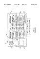
- FIG. 3 depicts a data processing system 140 constructed in accordance with the teachings of the present invention.
- data processing system 140 mounted on PC board 142, comprises processor 144 coupled to memory controller 148 which in turn is coupled to synchronous RAM 150.
- Processor 144, memory controller 148 and synchronous memory 150 work synchronously with clock signal "sysclk" 151 generated by system clock 154.
- processor 144 receives memory access requests which are then forwarded to memory controller 148.
- Memory controller 148 controls access to synchronous memory 150 and is responsible for processing memory access requests received from processor 144.
- Memory controller 148 comprises controller clock circuit 152 which receives system clock signal “sysclk” 151 generated by system clock 154, control signal logic circuit 153 which receives control signals 166 generated by processor 144 in response to a memory read/write command, address buffer 156 to store the memory address whose contents are to be read from or written to, data buffer 158 to store data read from synchronous memory 150, and programmable delay module 160 to provide a skewed timing signal (“skewclk”) 162 to data buffer 158.
- Controller clock circuit 152 provides system clock signal "sysclk” 151 to control signal logic circuit 153 and address buffer 156 without any modification.
- Control signals 166 include signals such as the row address strobe (RAS), the column address strobe (CAS) and the read/write enable (RWEN/WEN) signals which are required to perform memory access operations.
- RAS row address strobe
- CAS column address strobe
- RWEN/WEN read/write enable
- synchronous memory 150 comprises memory clock circuit 168 which receives "sysclk” system clock signal 151 from memory controller 148 via pads 164a and 176a, memory control signal logic circuit 170 which receives control signals 166 from memory controller 148 via pads 164b and 176b, address decoder 172 which receives the memory address from memory controller 148 via pads 164c and 176c, and memory data buffer 174 which stores the memory contents.
- memory clock circuit 168 provides "sysclk” signal 151 to memory control signal logic circuit 170, address decoder 172 and memory data buffer 174 without any modification.
- Address decoder 172 parses the memory address into a row address component and a column address component.
- data read from synchronous memory 150 is clocked into data buffer 158 in memory controller 148.
- data buffer 158 is clocked by system time control signal “sysclk” generated by the system clock
- data buffer 158 is clocked by a skewed timing clock pulse “skewclk” 162 generated by programmable delay module 160.
- Skwclk signal 162 is essentially “sysclk” signal 151 with a programmable delay added to it.
- FIG. 4 depicts a timing diagram showing the increased data valid window time provided in accordance with an embodiment of the present invention.
- valid data is clocked in by memory controller 148 at rising edge 181 of skewed timing signal "skewclk” generated by programmable delay module 160.
- the present invention extends the data valid window (t dv ) by a time amount equal to the delay (t skew ) added by programmable delay module 160.
- the length of t skew is programmed to allow sufficient set up and hold time for memory controller 148 to clock in valid data.
- the timing for memory controller 148 can be tuned to meet the setup and hold time required by data buffer 158 in memory controller 148.
- Factors used to determine the length of t skew value include the system clock frequency, speed ratings of synchronous memory 150, routing specifications of the PC board, and the memory "load" of the data processing system.
- FIG. 5 depicts the internal structure of programmable delay module 160 according to one embodiment of the present invention.
- programmable delay module 160 comprises input signal 180, delay lines 184a,b,c,d comprising of delay elements 182a,b,c,d,e,f, delay line selector 186 and output signal "skewclk” 162.
- Input signal 180 is connected via pad 164e to PC board trace 178 relaying the system clock signal between connecting pads 164a and 176a.
- the embodiment of the present invention depicted in FIG. 4 takes advantage of time delay "t mcd " required to route the system time signal "sysclk" from the memory controller to pad 164a.
- input signal 180 may be connected to any connector relaying the system time clock "sysclk" signal.
- this connector is the trace from clock controller circuit 152 to pad 164a.
- the value of t skew can also be reduced by careful layout of the components of the data processing system to reduce capacitance between the lead connections on the PC board.
- Delay elements 182a,b,c,d,e,f each add a finite amount of time delay to input signal 180.
- the value of t skew is directly proportional to the number of finite delays added by the delay elements.
- delay lines 184a,b,c,d represent lines of differing t skew values, with delay line 184a representing the minimum t skew value and line 184d representing the maximum t skew value.
- Delay line selector 186 determines which of the multiple delay lines is chosen as the "skewclk" signal and forwarded to data buffer 158. The selection of the appropriate delay line by delay line selector 186 is programmed using skew selection lines 188.
- t skew depends upon various factors such as system clock frequency, speed ratings of synchronous memory 150, metal trace layout specifications of the PC board, and the memory "load" of the data processing system.
- the present invention provides system designers with the flexibility to alter the t skew value using skew selection lines 188 depending on the above mentioned factors and other system requirements.
Landscapes
- Engineering & Computer Science (AREA)
- Theoretical Computer Science (AREA)
- Physics & Mathematics (AREA)
- General Engineering & Computer Science (AREA)
- General Physics & Mathematics (AREA)
- Dram (AREA)
Abstract
Description
              TABLE 1
______________________________________
"Routing access time" delays
Delay
Period
      Delay Name   Description of Delay
______________________________________
t.sub.mcd
      Memory controller
                   This represents the time delay required
      routing delay
                   to route the "read" command signals
                   from memory controller 106 to pads
                   124a, b, c.
t.sub.pcrd
      PC board routing
                   This represents the time delay required
      delay        to route the "read" command signals on
                   PC board 102 from pads 124a, b, c to
                   pads 134a, b, c.
t.sub.mrd
      Memory routing
                   This represents the time delay required
      delay        to route the "read" command signals
                   from pads 134a, b, c to memory clock
                   circuit 126, memory control signal logic
                   circuit 128 and address decoder 130,
                   respectively.
t.sub.macd
      Memory access
                   This represents the time delay required
      delay        to access the contents of memory data
                   buffer 132 in response to the row and
                   column addresses provided by address
                   decoder 130 and time delay required to
                   route the data to pad 134d.
t.sub.pcrd
      PC board routing
                   This represents the time delay required
      delay        to route the data read from
                   synchronous memory 108 from pad
                   134d to pad 124d on PC board 102.
t.sub.dbrd
      Data buffer routing
                   This represents the delay required to
      delay        route the data from pad 124d to data
                   buffer 120 in memory controller 106.
______________________________________
Claims (5)
Priority Applications (1)
| Application Number | Priority Date | Filing Date | Title |
|---|---|---|---|
| US09/274,568 US6131149A (en) | 1997-06-04 | 1999-03-23 | Apparatus and method for reading data from synchronous memory with skewed clock pulses |
Applications Claiming Priority (2)
| Application Number | Priority Date | Filing Date | Title |
|---|---|---|---|
| US08/869,083 US5946712A (en) | 1997-06-04 | 1997-06-04 | Apparatus and method for reading data from synchronous memory |
| US09/274,568 US6131149A (en) | 1997-06-04 | 1999-03-23 | Apparatus and method for reading data from synchronous memory with skewed clock pulses |
Related Parent Applications (1)
| Application Number | Title | Priority Date | Filing Date |
|---|---|---|---|
| US08/869,083 Continuation US5946712A (en) | 1997-06-04 | 1997-06-04 | Apparatus and method for reading data from synchronous memory |
Publications (1)
| Publication Number | Publication Date |
|---|---|
| US6131149A true US6131149A (en) | 2000-10-10 |
Family
ID=25352892
Family Applications (2)
| Application Number | Title | Priority Date | Filing Date |
|---|---|---|---|
| US08/869,083 Expired - Lifetime US5946712A (en) | 1997-06-04 | 1997-06-04 | Apparatus and method for reading data from synchronous memory |
| US09/274,568 Expired - Lifetime US6131149A (en) | 1997-06-04 | 1999-03-23 | Apparatus and method for reading data from synchronous memory with skewed clock pulses |
Family Applications Before (1)
| Application Number | Title | Priority Date | Filing Date |
|---|---|---|---|
| US08/869,083 Expired - Lifetime US5946712A (en) | 1997-06-04 | 1997-06-04 | Apparatus and method for reading data from synchronous memory |
Country Status (2)
| Country | Link |
|---|---|
| US (2) | US5946712A (en) |
| WO (1) | WO1998055935A1 (en) |
Cited By (63)
| Publication number | Priority date | Publication date | Assignee | Title |
|---|---|---|---|---|
| US6292903B1 (en) * | 1997-07-09 | 2001-09-18 | International Business Machines Corporation | Smart memory interface |
| US6397312B1 (en) * | 1997-07-04 | 2002-05-28 | Fujitsu Limited | Memory subsystem operated in synchronism with a clock |
| US20020161968A1 (en) * | 2001-02-09 | 2002-10-31 | Samsung Electronics Co., Ltd. | Memory system having stub bus configuration |
| US20020169994A1 (en) * | 2001-04-27 | 2002-11-14 | Ching-Yuan Yang | One-wire approach and its circuit for clock-skew compensating |
| US20030025540A1 (en) * | 2001-07-30 | 2003-02-06 | Elpida Memory, Inc. | Register capable of corresponding to wide frequency band and signal generating method using the same |
| EP1202282A3 (en) * | 2000-10-27 | 2003-05-21 | Infineon Technologies AG | Integrated memory with row line access control for asserting or de-asserting row conductors |
| US20030117864A1 (en) * | 2001-10-22 | 2003-06-26 | Hampel Craig E. | Phase adjustment apparatus and method for a memory device signaling system |
| US6611905B1 (en) * | 2000-06-29 | 2003-08-26 | International Business Machines Corporation | Memory interface with programable clock to output time based on wide range of receiver loads |
| US20030179644A1 (en) * | 2002-03-19 | 2003-09-25 | Ali Anvar | Synchronous global controller for enhanced pipelining |
| WO2004008326A3 (en) * | 2002-07-15 | 2004-04-08 | Globespan Virata Inc | System and method for improved synchronous data access |
| US20050057292A1 (en) * | 1999-07-14 | 2005-03-17 | Rambus Inc. | Apparatus and method for controlling a master/slave system via master device synchronization |
| US20050066136A1 (en) * | 2003-09-18 | 2005-03-24 | Schnepper Randy L. | Memory hub with integrated non-volatile memory |
| US20050083095A1 (en) * | 2003-10-16 | 2005-04-21 | Tsvika Kurts | Adaptive input/output buffer and methods thereof |
| US20050132159A1 (en) * | 2002-08-16 | 2005-06-16 | Jeddeloh Joseph M. | Memory hub bypass circuit and method |
| US20050146943A1 (en) * | 2003-08-28 | 2005-07-07 | Jeddeloh Joseph M. | Memory module and method having on-board data search capabilities and processor-based system using such memory modules |
| JP2005196479A (en) * | 2004-01-07 | 2005-07-21 | Ricoh Co Ltd | Memory control device |
| US6980042B2 (en) | 2004-04-05 | 2005-12-27 | Micron Technology, Inc. | Delay line synchronizer apparatus and method |
| US20060104313A1 (en) * | 2004-11-18 | 2006-05-18 | Mark Haner | Method and apparatus for timeout reduction and improved wireless network performance by delay injection |
| US20060120409A1 (en) * | 1999-10-19 | 2006-06-08 | Zerbe Jared L | Calibrated data communication system and method |
| US7106611B2 (en) * | 2002-09-09 | 2006-09-12 | Micron Technology, Inc. | Wavelength division multiplexed memory module, memory system and method |
| US7117316B2 (en) | 2002-08-05 | 2006-10-03 | Micron Technology, Inc. | Memory hub and access method having internal row caching |
| US7120723B2 (en) | 2004-03-25 | 2006-10-10 | Micron Technology, Inc. | System and method for memory hub-based expansion bus |
| US7120727B2 (en) | 2003-06-19 | 2006-10-10 | Micron Technology, Inc. | Reconfigurable memory module and method |
| US7120743B2 (en) | 2003-10-20 | 2006-10-10 | Micron Technology, Inc. | Arbitration system and method for memory responses in a hub-based memory system |
| US7133991B2 (en) | 2003-08-20 | 2006-11-07 | Micron Technology, Inc. | Method and system for capturing and bypassing memory transactions in a hub-based memory system |
| US7133972B2 (en) | 2002-06-07 | 2006-11-07 | Micron Technology, Inc. | Memory hub with internal cache and/or memory access prediction |
| US20060277345A1 (en) * | 1997-09-26 | 2006-12-07 | Haw-Jyh Liaw | High Frequency Bus System |
| US7181584B2 (en) | 2004-02-05 | 2007-02-20 | Micron Technology, Inc. | Dynamic command and/or address mirroring system and method for memory modules |
| US7180522B2 (en) | 2000-06-23 | 2007-02-20 | Micron Technology, Inc. | Apparatus and method for distributed memory control in a graphics processing system |
| US7188219B2 (en) | 2004-01-30 | 2007-03-06 | Micron Technology, Inc. | Buffer control system and method for a memory system having outstanding read and write request buffers |
| US20070058478A1 (en) * | 2005-09-06 | 2007-03-15 | Nec Electronics Corporation | Interface circuit |
| US7200024B2 (en) | 2002-08-02 | 2007-04-03 | Micron Technology, Inc. | System and method for optically interconnecting memory devices |
| US7210059B2 (en) | 2003-08-19 | 2007-04-24 | Micron Technology, Inc. | System and method for on-board diagnostics of memory modules |
| US7213082B2 (en) | 2004-03-29 | 2007-05-01 | Micron Technology, Inc. | Memory hub and method for providing memory sequencing hints |
| US7222213B2 (en) | 2004-05-17 | 2007-05-22 | Micron Technology, Inc. | System and method for communicating the synchronization status of memory modules during initialization of the memory modules |
| US7222197B2 (en) | 2003-07-22 | 2007-05-22 | Micron Technology, Inc. | Apparatus and method for direct memory access in a hub-based memory system |
| US7234070B2 (en) | 2003-10-27 | 2007-06-19 | Micron Technology, Inc. | System and method for using a learning sequence to establish communications on a high-speed nonsynchronous interface in the absence of clock forwarding |
| US7242213B2 (en) | 2003-06-11 | 2007-07-10 | Micron Technology, Inc. | Memory module and method having improved signal routing topology |
| US7254331B2 (en) | 2002-08-09 | 2007-08-07 | Micron Technology, Inc. | System and method for multiple bit optical data transmission in memory systems |
| US7257683B2 (en) | 2004-03-24 | 2007-08-14 | Micron Technology, Inc. | Memory arbitration system and method having an arbitration packet protocol |
| US7260685B2 (en) | 2003-06-20 | 2007-08-21 | Micron Technology, Inc. | Memory hub and access method having internal prefetch buffers |
| US7301831B2 (en) | 2004-09-15 | 2007-11-27 | Rambus Inc. | Memory systems with variable delays for write data signals |
| US7310748B2 (en) | 2004-06-04 | 2007-12-18 | Micron Technology, Inc. | Memory hub tester interface and method for use thereof |
| US7363419B2 (en) | 2004-05-28 | 2008-04-22 | Micron Technology, Inc. | Method and system for terminating write commands in a hub-based memory system |
| US7366864B2 (en) | 2004-03-08 | 2008-04-29 | Micron Technology, Inc. | Memory hub architecture having programmable lane widths |
| US7392331B2 (en) | 2004-08-31 | 2008-06-24 | Micron Technology, Inc. | System and method for transmitting data packets in a computer system having a memory hub architecture |
| US7397725B2 (en) | 1999-10-19 | 2008-07-08 | Rambus Inc. | Single-clock, strobeless signaling system |
| DE10235739B4 (en) * | 2001-07-30 | 2008-08-14 | Elpida Memory, Inc. | Register mounted on a memory module and use of a register in a memory module |
| US7428644B2 (en) | 2003-06-20 | 2008-09-23 | Micron Technology, Inc. | System and method for selective memory module power management |
| US7447240B2 (en) | 2004-03-29 | 2008-11-04 | Micron Technology, Inc. | Method and system for synchronizing communications links in a hub-based memory system |
| US7484064B2 (en) | 2001-04-24 | 2009-01-27 | Rambus Inc. | Method and apparatus for signaling between devices of a memory system |
| US7519788B2 (en) | 2004-06-04 | 2009-04-14 | Micron Technology, Inc. | System and method for an asynchronous data buffer having buffer write and read pointers |
| US20090129178A1 (en) * | 1997-10-10 | 2009-05-21 | Barth Richard M | Integrated Circuit Memory Device Having Delayed Write Timing Based on Read Response Time |
| US7590797B2 (en) | 2004-04-08 | 2009-09-15 | Micron Technology, Inc. | System and method for optimizing interconnections of components in a multichip memory module |
| KR100920179B1 (en) * | 2008-04-11 | 2009-10-06 | 인하대학교 산학협력단 | Memory controller |
| US7657877B2 (en) | 2001-06-20 | 2010-02-02 | Pact Xpp Technologies Ag | Method for processing data |
| US7788451B2 (en) | 2004-02-05 | 2010-08-31 | Micron Technology, Inc. | Apparatus and method for data bypass for a bi-directional data bus in a hub-based memory sub-system |
| US7805586B2 (en) | 2002-08-29 | 2010-09-28 | Micron Technology, Inc. | System and method for optimizing interconnections of memory devices in a multichip module |
| US8127061B2 (en) | 2002-02-18 | 2012-02-28 | Martin Vorbach | Bus systems and reconfiguration methods |
| US8320202B2 (en) | 2001-04-24 | 2012-11-27 | Rambus Inc. | Clocked memory system with termination component |
| US8392768B2 (en) | 2010-06-03 | 2013-03-05 | Sunplus Technology Co., Ltd. | Memory test system with advance features for completed memory system |
| US8880833B2 (en) | 2003-12-29 | 2014-11-04 | Micron Technology, Inc. | System and method for read synchronization of memory modules |
| US9177623B2 (en) | 2013-03-15 | 2015-11-03 | Qualcomm Incorporated | Memory interface offset signaling |
Families Citing this family (25)
| Publication number | Priority date | Publication date | Assignee | Title |
|---|---|---|---|---|
| JP3097737B2 (en) * | 1997-01-27 | 2000-10-10 | 日本電気株式会社 | Memory circuit for burst clock |
| US6480548B1 (en) * | 1997-11-17 | 2002-11-12 | Silicon Graphics, Inc. | Spacial derivative bus encoder and decoder |
| US6154509A (en) * | 1998-01-16 | 2000-11-28 | Natural Microsystems Corp. | Data phase recovery system |
| US6253333B1 (en) * | 1998-03-23 | 2001-06-26 | International Business Machines Corporation | Apparatus and method for testing programmable delays |
| JPH11340421A (en) * | 1998-05-25 | 1999-12-10 | Fujitsu Ltd | LSI device with mixed memory and logic |
| EP1156420B1 (en) * | 1998-12-15 | 2005-07-06 | Matsushita Electric Industrial Co., Ltd. | Clock phase adjustment method, and integrated circuit and design method therefor |
| DE10048895A1 (en) * | 1999-10-01 | 2001-06-13 | Schlumberger Technologies Inc | Testing method for electronic components that outputs a source-synchronized signal using an automatic test device by introduction of a time delay into the output signal and output clock signal to allow time balancing of path length errors |
| KR100316718B1 (en) * | 1999-12-13 | 2001-12-12 | 윤종용 | Skew insensitive data receiver |
| US7031420B1 (en) * | 1999-12-30 | 2006-04-18 | Silicon Graphics, Inc. | System and method for adaptively deskewing parallel data signals relative to a clock |
| JP2002082830A (en) | 2000-02-14 | 2002-03-22 | Mitsubishi Electric Corp | Interface circuit |
| US6578125B2 (en) * | 2000-02-14 | 2003-06-10 | Sanyo Electric Co., Ltd. | Memory access circuit and memory access control circuit |
| KR100389916B1 (en) * | 2000-08-28 | 2003-07-04 | 삼성전자주식회사 | Memory module and memory controller |
| US6530006B1 (en) * | 2000-09-18 | 2003-03-04 | Intel Corporation | System and method for providing reliable transmission in a buffered memory system |
| JP2002108693A (en) * | 2000-10-03 | 2002-04-12 | Fujitsu Ltd | Data reading method, memory controller and semiconductor integrated circuit device |
| KR100378194B1 (en) * | 2001-02-19 | 2003-03-29 | 삼성전자주식회사 | Memory module for controlling set up and hold time of input signal of semiconductor memory device and method thereof |
| US6904551B1 (en) * | 2001-02-20 | 2005-06-07 | Cypress Semiconductor Corporation | Method and circuit for setup and hold detect pass-fail test mode |
| KR100562504B1 (en) * | 2003-08-29 | 2006-03-21 | 삼성전자주식회사 | Semiconductor memory device to reduce phase difference of signal |
| DE102004013929B3 (en) * | 2004-03-22 | 2005-08-11 | Infineon Technologies Ag | Control method for the reading in of a data signal to an electronic circuit input latch, especially to a DRAM circuit, whereby the delay between signal and clock flanks is set so that it is within a defined time window |
| US7457978B2 (en) * | 2005-05-09 | 2008-11-25 | Micron Technology, Inc. | Adjustable byte lane offset for memory module to reduce skew |
| US7471130B2 (en) * | 2005-05-19 | 2008-12-30 | Micron Technology, Inc. | Graduated delay line for increased clock skew correction circuit operating range |
| US20080129357A1 (en) * | 2006-11-30 | 2008-06-05 | Chlipala James D | Adaptive Integrated Circuit Clock Skew Correction |
| US8665665B2 (en) | 2011-03-30 | 2014-03-04 | Mediatek Inc. | Apparatus and method to adjust clock duty cycle of memory |
| US9076558B2 (en) * | 2012-11-01 | 2015-07-07 | Nanya Technology Corporation | Memory test system and memory test method |
| CN110797076B (en) * | 2019-10-16 | 2021-09-14 | 中国科学院微电子研究所 | NAND Flash time sequence testing method |
| US20230288953A1 (en) * | 2022-03-09 | 2023-09-14 | Oppstar Technology Sdn Bhd | Adjustable clock phase for peak-current reduction |
Citations (9)
| Publication number | Priority date | Publication date | Assignee | Title |
|---|---|---|---|---|
| US4739277A (en) * | 1986-03-03 | 1988-04-19 | Tektronix, Inc. | Triggered, programmable skew signal generator |
| EP0339224A2 (en) * | 1988-04-29 | 1989-11-02 | International Business Machines Corporation | Memory controller |
| US5255383A (en) * | 1991-04-15 | 1993-10-19 | Seagate Technology, Inc. | Method and apparatus for skewing a memory read clock signal in a magnetic disk drive system |
| US5560000A (en) * | 1992-05-28 | 1996-09-24 | Texas Instruments Incorporated | Time skewing arrangement for operating memory in synchronism with a data processor |
| US5577236A (en) * | 1994-12-30 | 1996-11-19 | International Business Machines Corporation | Memory controller for reading data from synchronous RAM |
| US5623638A (en) * | 1994-11-22 | 1997-04-22 | Advanced Micro Devices, Inc. | Memory control unit with programmable edge generator to minimize delay periods for critical DRAM timing parameters |
| US5812472A (en) * | 1997-07-16 | 1998-09-22 | Tanisys Technology, Inc. | Nested loop method of identifying synchronous memories |
| US5815016A (en) * | 1994-09-02 | 1998-09-29 | Xilinx, Inc. | Phase-locked delay loop for clock correction |
| US5886948A (en) * | 1996-12-20 | 1999-03-23 | Micron Technology, Inc. | Memory having a plurality of external clock signal inputs |
-
1997
- 1997-06-04 US US08/869,083 patent/US5946712A/en not_active Expired - Lifetime
-
1998
- 1998-05-04 WO PCT/US1998/009011 patent/WO1998055935A1/en not_active Ceased
-
1999
- 1999-03-23 US US09/274,568 patent/US6131149A/en not_active Expired - Lifetime
Patent Citations (10)
| Publication number | Priority date | Publication date | Assignee | Title |
|---|---|---|---|---|
| US4739277A (en) * | 1986-03-03 | 1988-04-19 | Tektronix, Inc. | Triggered, programmable skew signal generator |
| EP0339224A2 (en) * | 1988-04-29 | 1989-11-02 | International Business Machines Corporation | Memory controller |
| US5255383A (en) * | 1991-04-15 | 1993-10-19 | Seagate Technology, Inc. | Method and apparatus for skewing a memory read clock signal in a magnetic disk drive system |
| US5560000A (en) * | 1992-05-28 | 1996-09-24 | Texas Instruments Incorporated | Time skewing arrangement for operating memory in synchronism with a data processor |
| US5608896A (en) * | 1992-05-28 | 1997-03-04 | Texas Instruments Incorporated | Time skewing arrangement for operating memory devices in synchronism with a data processor |
| US5815016A (en) * | 1994-09-02 | 1998-09-29 | Xilinx, Inc. | Phase-locked delay loop for clock correction |
| US5623638A (en) * | 1994-11-22 | 1997-04-22 | Advanced Micro Devices, Inc. | Memory control unit with programmable edge generator to minimize delay periods for critical DRAM timing parameters |
| US5577236A (en) * | 1994-12-30 | 1996-11-19 | International Business Machines Corporation | Memory controller for reading data from synchronous RAM |
| US5886948A (en) * | 1996-12-20 | 1999-03-23 | Micron Technology, Inc. | Memory having a plurality of external clock signal inputs |
| US5812472A (en) * | 1997-07-16 | 1998-09-22 | Tanisys Technology, Inc. | Nested loop method of identifying synchronous memories |
Non-Patent Citations (1)
| Title |
|---|
| PCT International Search Report Dated Sep. 10, 1998. * |
Cited By (232)
| Publication number | Priority date | Publication date | Assignee | Title |
|---|---|---|---|---|
| US6397312B1 (en) * | 1997-07-04 | 2002-05-28 | Fujitsu Limited | Memory subsystem operated in synchronism with a clock |
| US6292903B1 (en) * | 1997-07-09 | 2001-09-18 | International Business Machines Corporation | Smart memory interface |
| US8364878B2 (en) | 1997-09-26 | 2013-01-29 | Rambus Inc. | Memory module having signal lines configured for sequential arrival of signals at a plurality of memory devices |
| US20060277345A1 (en) * | 1997-09-26 | 2006-12-07 | Haw-Jyh Liaw | High Frequency Bus System |
| US20090210604A1 (en) * | 1997-09-26 | 2009-08-20 | Haw-Jyh Liaw | Memory Module Having Signal Lines Configured for Sequential Arrival of Signals at Synchronous Memory Devices |
| US20070150635A1 (en) * | 1997-09-26 | 2007-06-28 | Haw-Jyh Liaw | Memory System Having Memory Devices on Two Sides |
| US7870322B2 (en) | 1997-09-26 | 2011-01-11 | Rambus Inc. | Memory module having signal lines configured for sequential arrival of signals at synchronous memory devices |
| US20070150636A1 (en) * | 1997-09-26 | 2007-06-28 | Haw-Jyh Liaw | Memory Module Having a Clock Line and Termination |
| US20110090727A1 (en) * | 1997-09-26 | 2011-04-21 | Haw-Jyh Liaw | Memory Module Having Signal Lines Configured for Sequential Arrival of Signals at Synchronous Memory Devices |
| US20070216800A1 (en) * | 1997-09-26 | 2007-09-20 | Haw-Jyh Liaw | Memory System Having a Clock Line and Termination |
| US7523244B2 (en) | 1997-09-26 | 2009-04-21 | Rambus Inc. | Memory module having memory devices on two sides |
| US8214575B2 (en) | 1997-09-26 | 2012-07-03 | Rambus Inc. | Memory module having signal lines configured for sequential arrival of signals at synchronous memory devices |
| US7523246B2 (en) | 1997-09-26 | 2009-04-21 | Rambus Inc. | Memory system having memory devices on two sides |
| US7523247B2 (en) | 1997-09-26 | 2009-04-21 | Rambus Inc. | Memory module having a clock line and termination |
| US7519757B2 (en) | 1997-09-26 | 2009-04-14 | Rambus Inc. | Memory system having a clock line and termination |
| US20090129178A1 (en) * | 1997-10-10 | 2009-05-21 | Barth Richard M | Integrated Circuit Memory Device Having Delayed Write Timing Based on Read Response Time |
| US7793039B2 (en) | 1997-10-10 | 2010-09-07 | Rambus Inc. | Interface for a semiconductor memory device and method for controlling the interface |
| US8560797B2 (en) | 1997-10-10 | 2013-10-15 | Rambus Inc. | Method and apparatus for indicating mask information |
| US8019958B2 (en) | 1997-10-10 | 2011-09-13 | Rambus Inc. | Memory write signaling and methods thereof |
| US8205056B2 (en) | 1997-10-10 | 2012-06-19 | Rambus Inc. | Memory controller for controlling write signaling |
| US20080013662A1 (en) * | 1999-07-14 | 2008-01-17 | Stefanos Sidiropoulos | Master Device with Time Domains for Slave Devices in Synchronous Memory System |
| US20050057292A1 (en) * | 1999-07-14 | 2005-03-17 | Rambus Inc. | Apparatus and method for controlling a master/slave system via master device synchronization |
| US7489756B2 (en) | 1999-07-14 | 2009-02-10 | Rambus Inc. | Slave device with calibration signal generator for synchronous memory system |
| US8428210B2 (en) | 1999-07-14 | 2013-04-23 | Rambus Inc. | Apparatus and method for controlling a master/slave system via master device synchronization |
| US20090045854A1 (en) * | 1999-07-14 | 2009-02-19 | Stefanos Sidiropoulos | Apparatus and Method for Controlling a Master/Slave System via Master Device Synchronization |
| US20070258554A1 (en) * | 1999-07-14 | 2007-11-08 | Stefanos Sidiropoulos | Slave Device with Calibration Signal Generator for Synchronous Memory System |
| US7702057B2 (en) | 1999-07-14 | 2010-04-20 | Rambus Inc. | Apparatus and method for controlling a master/slave system via master device synchronization |
| US20070258555A1 (en) * | 1999-07-14 | 2007-11-08 | Stefanos Sidiropoulos | Slave Device with Synchronous Interface for Use in Synchronous Memory System |
| US7466784B2 (en) * | 1999-07-14 | 2008-12-16 | Rambus Inc. | Apparatus and method for controlling a master/slave system via master device synchronization |
| US7548601B2 (en) | 1999-07-14 | 2009-06-16 | Rambus Inc. | Slave device with synchronous interface for use in synchronous memory system |
| US7570726B2 (en) * | 1999-07-14 | 2009-08-04 | Rambus Inc. | Master device with time domains for slave devices in synchronous memory system |
| US8102730B2 (en) | 1999-10-19 | 2012-01-24 | Rambus, Inc. | Single-clock, strobeless signaling system |
| US9164933B2 (en) | 1999-10-19 | 2015-10-20 | Rambus Inc. | Memory system with calibrated data communication |
| US20090327789A1 (en) * | 1999-10-19 | 2009-12-31 | Zerbe Jared Levan | Memory System with Calibrated Data Communication |
| US9405678B2 (en) | 1999-10-19 | 2016-08-02 | Rambus Inc. | Flash memory controller with calibrated data communication |
| US7663966B2 (en) | 1999-10-19 | 2010-02-16 | Rambus, Inc. | Single-clock, strobeless signaling system |
| US8948212B2 (en) | 1999-10-19 | 2015-02-03 | Rambus Inc. | Memory controller with circuitry to set memory device-specific reference voltages |
| US7397725B2 (en) | 1999-10-19 | 2008-07-08 | Rambus Inc. | Single-clock, strobeless signaling system |
| US7535933B2 (en) | 1999-10-19 | 2009-05-19 | Rambus Inc. | Calibrated data communication system and method |
| US9785589B2 (en) | 1999-10-19 | 2017-10-10 | Rambus Inc. | Memory controller that calibrates a transmit timing offset |
| US20060120409A1 (en) * | 1999-10-19 | 2006-06-08 | Zerbe Jared L | Calibrated data communication system and method |
| US8170067B2 (en) | 1999-10-19 | 2012-05-01 | Rambus Inc. | Memory system with calibrated data communication |
| US10310999B2 (en) | 1999-10-19 | 2019-06-04 | Rambus Inc. | Flash memory controller with calibrated data communication |
| US8630317B2 (en) | 1999-10-19 | 2014-01-14 | Rambus Inc. | Memory system with calibrated data communication |
| US7180522B2 (en) | 2000-06-23 | 2007-02-20 | Micron Technology, Inc. | Apparatus and method for distributed memory control in a graphics processing system |
| US6611905B1 (en) * | 2000-06-29 | 2003-08-26 | International Business Machines Corporation | Memory interface with programable clock to output time based on wide range of receiver loads |
| EP1202282A3 (en) * | 2000-10-27 | 2003-05-21 | Infineon Technologies AG | Integrated memory with row line access control for asserting or de-asserting row conductors |
| US20020161968A1 (en) * | 2001-02-09 | 2002-10-31 | Samsung Electronics Co., Ltd. | Memory system having stub bus configuration |
| US7313715B2 (en) | 2001-02-09 | 2007-12-25 | Samsung Electronics Co., Ltd. | Memory system having stub bus configuration |
| US10706910B2 (en) | 2001-04-24 | 2020-07-07 | Rambus Inc. | Memory controller |
| US9741424B2 (en) | 2001-04-24 | 2017-08-22 | Rambus Inc. | Memory controller |
| US9053778B2 (en) | 2001-04-24 | 2015-06-09 | Rambus Inc. | Memory controller that enforces strobe-to-strobe timing offset |
| US8625371B2 (en) | 2001-04-24 | 2014-01-07 | Rambus Inc. | Memory component with terminated and unterminated signaling inputs |
| US8717837B2 (en) | 2001-04-24 | 2014-05-06 | Rambus Inc. | Memory module |
| US8320202B2 (en) | 2001-04-24 | 2012-11-27 | Rambus Inc. | Clocked memory system with termination component |
| US7484064B2 (en) | 2001-04-24 | 2009-01-27 | Rambus Inc. | Method and apparatus for signaling between devices of a memory system |
| US9311976B2 (en) | 2001-04-24 | 2016-04-12 | Rambus Inc. | Memory module |
| US8359445B2 (en) | 2001-04-24 | 2013-01-22 | Rambus Inc. | Method and apparatus for signaling between devices of a memory system |
| US8391039B2 (en) | 2001-04-24 | 2013-03-05 | Rambus Inc. | Memory module with termination component |
| US8395951B2 (en) | 2001-04-24 | 2013-03-12 | Rambus Inc. | Memory controller |
| US10236051B2 (en) | 2001-04-24 | 2019-03-19 | Rambus Inc. | Memory controller |
| US8537601B2 (en) | 2001-04-24 | 2013-09-17 | Rambus Inc. | Memory controller with selective data transmission delay |
| US8214616B2 (en) | 2001-04-24 | 2012-07-03 | Rambus Inc. | Memory controller device having timing offset capability |
| US8462566B2 (en) | 2001-04-24 | 2013-06-11 | Rambus Inc. | Memory module with termination component |
| US8760944B2 (en) | 2001-04-24 | 2014-06-24 | Rambus Inc. | Memory component that samples command/address signals in response to both edges of a clock signal |
| US9472262B2 (en) | 2001-04-24 | 2016-10-18 | Rambus Inc. | Memory controller |
| US20020169994A1 (en) * | 2001-04-27 | 2002-11-14 | Ching-Yuan Yang | One-wire approach and its circuit for clock-skew compensating |
| US6754841B2 (en) * | 2001-04-27 | 2004-06-22 | Archic Technology Corporation | One-wire approach and its circuit for clock-skew compensating |
| US7657877B2 (en) | 2001-06-20 | 2010-02-02 | Pact Xpp Technologies Ag | Method for processing data |
| US6986072B2 (en) | 2001-07-30 | 2006-01-10 | Elpida Memory, Inc. | Register capable of corresponding to wide frequency band and signal generating method using the same |
| US20030025540A1 (en) * | 2001-07-30 | 2003-02-06 | Elpida Memory, Inc. | Register capable of corresponding to wide frequency band and signal generating method using the same |
| DE10235739B4 (en) * | 2001-07-30 | 2008-08-14 | Elpida Memory, Inc. | Register mounted on a memory module and use of a register in a memory module |
| US10192609B2 (en) | 2001-10-22 | 2019-01-29 | Rambus Inc. | Memory component with pattern register circuitry to provide data patterns for calibration |
| US20030117864A1 (en) * | 2001-10-22 | 2003-06-26 | Hampel Craig E. | Phase adjustment apparatus and method for a memory device signaling system |
| US7398413B2 (en) * | 2001-10-22 | 2008-07-08 | Rambus Inc. | Memory device signaling system and method with independent timing calibration for parallel signal paths |
| US9367248B2 (en) | 2001-10-22 | 2016-06-14 | Rambus Inc. | Memory component with pattern register circuitry to provide data patterns for calibration |
| US7668276B2 (en) | 2001-10-22 | 2010-02-23 | Rambus Inc. | Phase adjustment apparatus and method for a memory device signaling system |
| US9123433B2 (en) | 2001-10-22 | 2015-09-01 | Rambus Inc. | Memory component with pattern register circuitry to provide data patterns for calibration |
| US9099194B2 (en) | 2001-10-22 | 2015-08-04 | Rambus Inc. | Memory component with pattern register circuitry to provide data patterns for calibration |
| US20090138747A1 (en) * | 2001-10-22 | 2009-05-28 | Hampel Craig E | Phase Adjustment Apparatus and Method for a Memory Device Signaling System |
| US11232827B2 (en) | 2001-10-22 | 2022-01-25 | Highlands, LLC | Memory component with pattern register circuitry to provide data patterns for calibration |
| US10811080B2 (en) | 2001-10-22 | 2020-10-20 | Rambus Inc. | Memory component with pattern register circuitry to provide data patterns for calibration |
| US7965567B2 (en) | 2001-10-22 | 2011-06-21 | Rambus Inc. | Phase adjustment apparatus and method for a memory device signaling system |
| US20050132158A1 (en) * | 2001-10-22 | 2005-06-16 | Rambus Inc. | Memory device signaling system and method with independent timing calibration for parallel signal paths |
| US9721642B2 (en) | 2001-10-22 | 2017-08-01 | Rambus Inc. | Memory component with pattern register circuitry to provide data patterns for calibration |
| US8542787B2 (en) | 2001-10-22 | 2013-09-24 | Rambus Inc. | Phase adjustment apparatus and method for a memory device signaling system |
| US8127061B2 (en) | 2002-02-18 | 2012-02-28 | Martin Vorbach | Bus systems and reconfiguration methods |
| US6928026B2 (en) * | 2002-03-19 | 2005-08-09 | Broadcom Corporation | Synchronous global controller for enhanced pipelining |
| US8149645B2 (en) * | 2002-03-19 | 2012-04-03 | Broadcom Corporation | Synchronous global controller for enhanced pipelining |
| US9159385B2 (en) | 2002-03-19 | 2015-10-13 | Broadcom Corporation | Memory architecture with local and global control circuitry |
| US20100185890A1 (en) * | 2002-03-19 | 2010-07-22 | Ali Anvar | Synchronous global controller for enhanced pipelining |
| US20030179644A1 (en) * | 2002-03-19 | 2003-09-25 | Ali Anvar | Synchronous global controller for enhanced pipelining |
| US9542997B2 (en) | 2002-03-19 | 2017-01-10 | Broadcom Corporation | Memory architecture with local and global control circuitry |
| US8693279B2 (en) | 2002-03-19 | 2014-04-08 | Broadcom Corporation | Synchronous global controller for enhanced pipelining |
| US8499127B2 (en) | 2002-06-07 | 2013-07-30 | Round Rock Research, Llc | Memory hub with internal cache and/or memory access prediction |
| US7945737B2 (en) | 2002-06-07 | 2011-05-17 | Round Rock Research, Llc | Memory hub with internal cache and/or memory access prediction |
| US7133972B2 (en) | 2002-06-07 | 2006-11-07 | Micron Technology, Inc. | Memory hub with internal cache and/or memory access prediction |
| US20110219196A1 (en) * | 2002-06-07 | 2011-09-08 | Round Rock Research, Llc | Memory hub with internal cache and/or memory access prediction |
| US7644253B2 (en) | 2002-06-07 | 2010-01-05 | Micron Technology, Inc. | Memory hub with internal cache and/or memory access prediction |
| US8195918B2 (en) | 2002-06-07 | 2012-06-05 | Round Rock Research, Llc | Memory hub with internal cache and/or memory access prediction |
| WO2004008326A3 (en) * | 2002-07-15 | 2004-04-08 | Globespan Virata Inc | System and method for improved synchronous data access |
| US7418616B2 (en) | 2002-07-15 | 2008-08-26 | Brooktree Broadband Holding, Inc. | System and method for improved synchronous data access |
| US7411807B2 (en) | 2002-08-02 | 2008-08-12 | Micron Technology, Inc. | System and method for optically interconnecting memory devices |
| US7382639B2 (en) | 2002-08-02 | 2008-06-03 | Micron Technology, Inc. | System and method for optically interconnecting memory devices |
| US7289347B2 (en) | 2002-08-02 | 2007-10-30 | Micron Technology, Inc. | System and method for optically interconnecting memory devices |
| US7200024B2 (en) | 2002-08-02 | 2007-04-03 | Micron Technology, Inc. | System and method for optically interconnecting memory devices |
| US8954687B2 (en) | 2002-08-05 | 2015-02-10 | Micron Technology, Inc. | Memory hub and access method having a sequencer and internal row caching |
| US7117316B2 (en) | 2002-08-05 | 2006-10-03 | Micron Technology, Inc. | Memory hub and access method having internal row caching |
| US7489875B2 (en) | 2002-08-09 | 2009-02-10 | Micron Technology, Inc. | System and method for multiple bit optical data transmission in memory systems |
| US7254331B2 (en) | 2002-08-09 | 2007-08-07 | Micron Technology, Inc. | System and method for multiple bit optical data transmission in memory systems |
| US20050132159A1 (en) * | 2002-08-16 | 2005-06-16 | Jeddeloh Joseph M. | Memory hub bypass circuit and method |
| US7415567B2 (en) | 2002-08-16 | 2008-08-19 | Micron Technology, Inc. | Memory hub bypass circuit and method |
| US7047351B2 (en) | 2002-08-16 | 2006-05-16 | Micron Technology, Inc. | Memory hub bypass circuit and method |
| US7149874B2 (en) | 2002-08-16 | 2006-12-12 | Micron Technology, Inc. | Memory hub bypass circuit and method |
| US7836252B2 (en) | 2002-08-29 | 2010-11-16 | Micron Technology, Inc. | System and method for optimizing interconnections of memory devices in a multichip module |
| US7805586B2 (en) | 2002-08-29 | 2010-09-28 | Micron Technology, Inc. | System and method for optimizing interconnections of memory devices in a multichip module |
| US8190819B2 (en) | 2002-08-29 | 2012-05-29 | Micron Technology, Inc. | System and method for optimizing interconnections of memory devices in a multichip module |
| US7106611B2 (en) * | 2002-09-09 | 2006-09-12 | Micron Technology, Inc. | Wavelength division multiplexed memory module, memory system and method |
| US7282947B2 (en) | 2003-06-11 | 2007-10-16 | Micron Technology, Inc. | Memory module and method having improved signal routing topology |
| US7242213B2 (en) | 2003-06-11 | 2007-07-10 | Micron Technology, Inc. | Memory module and method having improved signal routing topology |
| US7746095B2 (en) | 2003-06-11 | 2010-06-29 | Round Rock Research, Llc | Memory module and method having improved signal routing topology |
| US7557601B2 (en) | 2003-06-11 | 2009-07-07 | Micron Technology, Inc. | Memory module and method having improved signal routing topology |
| US7245145B2 (en) | 2003-06-11 | 2007-07-17 | Micron Technology, Inc. | Memory module and method having improved signal routing topology |
| US7818712B2 (en) | 2003-06-19 | 2010-10-19 | Round Rock Research, Llc | Reconfigurable memory module and method |
| US8732383B2 (en) | 2003-06-19 | 2014-05-20 | Round Rock Research, Llc | Reconfigurable memory module and method |
| US8200884B2 (en) | 2003-06-19 | 2012-06-12 | Round Rock Research, Llc | Reconfigurable memory module and method |
| US7966444B2 (en) | 2003-06-19 | 2011-06-21 | Round Rock Research, Llc | Reconfigurable memory module and method |
| US20110029746A1 (en) * | 2003-06-19 | 2011-02-03 | Round Rock Research, Llc | Reconfigurable memory module and method |
| US7120727B2 (en) | 2003-06-19 | 2006-10-10 | Micron Technology, Inc. | Reconfigurable memory module and method |
| US7412566B2 (en) | 2003-06-20 | 2008-08-12 | Micron Technology, Inc. | Memory hub and access method having internal prefetch buffers |
| US8127081B2 (en) | 2003-06-20 | 2012-02-28 | Round Rock Research, Llc | Memory hub and access method having internal prefetch buffers |
| US7428644B2 (en) | 2003-06-20 | 2008-09-23 | Micron Technology, Inc. | System and method for selective memory module power management |
| US7260685B2 (en) | 2003-06-20 | 2007-08-21 | Micron Technology, Inc. | Memory hub and access method having internal prefetch buffers |
| US7437579B2 (en) | 2003-06-20 | 2008-10-14 | Micron Technology, Inc. | System and method for selective memory module power management |
| US8209445B2 (en) | 2003-07-22 | 2012-06-26 | Round Rock Research, Llc | Apparatus and method for direct memory access in a hub-based memory system |
| US7966430B2 (en) | 2003-07-22 | 2011-06-21 | Round Rock Research, Llc | Apparatus and method for direct memory access in a hub-based memory system |
| US7389364B2 (en) | 2003-07-22 | 2008-06-17 | Micron Technology, Inc. | Apparatus and method for direct memory access in a hub-based memory system |
| US7222197B2 (en) | 2003-07-22 | 2007-05-22 | Micron Technology, Inc. | Apparatus and method for direct memory access in a hub-based memory system |
| US7278060B2 (en) | 2003-08-19 | 2007-10-02 | Micron Technology, Inc. | System and method for on-board diagnostics of memory modules |
| US7913122B2 (en) | 2003-08-19 | 2011-03-22 | Round Rock Research, Llc | System and method for on-board diagnostics of memory modules |
| US7516363B2 (en) | 2003-08-19 | 2009-04-07 | Micron Technology, Inc. | System and method for on-board diagnostics of memory modules |
| US7210059B2 (en) | 2003-08-19 | 2007-04-24 | Micron Technology, Inc. | System and method for on-board diagnostics of memory modules |
| US7251714B2 (en) | 2003-08-20 | 2007-07-31 | Micron Technology, Inc. | Method and system for capturing and bypassing memory transactions in a hub-based memory system |
| US7133991B2 (en) | 2003-08-20 | 2006-11-07 | Micron Technology, Inc. | Method and system for capturing and bypassing memory transactions in a hub-based memory system |
| US20050146943A1 (en) * | 2003-08-28 | 2005-07-07 | Jeddeloh Joseph M. | Memory module and method having on-board data search capabilities and processor-based system using such memory modules |
| US7975122B2 (en) | 2003-09-18 | 2011-07-05 | Round Rock Research, Llc | Memory hub with integrated non-volatile memory |
| US7490211B2 (en) | 2003-09-18 | 2009-02-10 | Micron Technology, Inc. | Memory hub with integrated non-volatile memory |
| US8832404B2 (en) | 2003-09-18 | 2014-09-09 | Round Rock Research, Llc | Memory hub with integrated non-volatile memory |
| US7194593B2 (en) | 2003-09-18 | 2007-03-20 | Micron Technology, Inc. | Memory hub with integrated non-volatile memory |
| US20050066136A1 (en) * | 2003-09-18 | 2005-03-24 | Schnepper Randy L. | Memory hub with integrated non-volatile memory |
| US20050083095A1 (en) * | 2003-10-16 | 2005-04-21 | Tsvika Kurts | Adaptive input/output buffer and methods thereof |
| WO2005038657A3 (en) * | 2003-10-16 | 2005-06-16 | Intel Corp | Adaptive input/output buffer and methods for use thereof |
| DE112004003057B4 (en) * | 2003-10-16 | 2011-09-15 | Intel Corporation | A controller and printed circuit comprising an input or output buffer and a programmable delay cell for converting clock delays |
| US7120743B2 (en) | 2003-10-20 | 2006-10-10 | Micron Technology, Inc. | Arbitration system and method for memory responses in a hub-based memory system |
| US8589643B2 (en) | 2003-10-20 | 2013-11-19 | Round Rock Research, Llc | Arbitration system and method for memory responses in a hub-based memory system |
| US7234070B2 (en) | 2003-10-27 | 2007-06-19 | Micron Technology, Inc. | System and method for using a learning sequence to establish communications on a high-speed nonsynchronous interface in the absence of clock forwarding |
| US7461286B2 (en) | 2003-10-27 | 2008-12-02 | Micron Technology, Inc. | System and method for using a learning sequence to establish communications on a high-speed nonsynchronous interface in the absence of clock forwarding |
| US8880833B2 (en) | 2003-12-29 | 2014-11-04 | Micron Technology, Inc. | System and method for read synchronization of memory modules |
| JP2005196479A (en) * | 2004-01-07 | 2005-07-21 | Ricoh Co Ltd | Memory control device |
| US7188219B2 (en) | 2004-01-30 | 2007-03-06 | Micron Technology, Inc. | Buffer control system and method for a memory system having outstanding read and write request buffers |
| US8788765B2 (en) | 2004-01-30 | 2014-07-22 | Micron Technology, Inc. | Buffer control system and method for a memory system having outstanding read and write request buffers |
| US8504782B2 (en) | 2004-01-30 | 2013-08-06 | Micron Technology, Inc. | Buffer control system and method for a memory system having outstanding read and write request buffers |
| US7181584B2 (en) | 2004-02-05 | 2007-02-20 | Micron Technology, Inc. | Dynamic command and/or address mirroring system and method for memory modules |
| US7546435B2 (en) | 2004-02-05 | 2009-06-09 | Micron Technology. Inc. | Dynamic command and/or address mirroring system and method for memory modules |
| US9164937B2 (en) | 2004-02-05 | 2015-10-20 | Micron Technology, Inc. | Apparatus and method for data bypass for a bi-directional data bus in a hub-based memory sub-system |
| US8291173B2 (en) | 2004-02-05 | 2012-10-16 | Micron Technology, Inc. | Apparatus and method for data bypass for a bi-directional data bus in a hub-based memory sub-system |
| US7788451B2 (en) | 2004-02-05 | 2010-08-31 | Micron Technology, Inc. | Apparatus and method for data bypass for a bi-directional data bus in a hub-based memory sub-system |
| US8694735B2 (en) | 2004-02-05 | 2014-04-08 | Micron Technology, Inc. | Apparatus and method for data bypass for a bi-directional data bus in a hub-based memory sub-system |
| US9274991B2 (en) | 2004-03-08 | 2016-03-01 | Micron Technology, Inc. | Memory hub architecture having programmable lane widths |
| US7366864B2 (en) | 2004-03-08 | 2008-04-29 | Micron Technology, Inc. | Memory hub architecture having programmable lane widths |
| US8775764B2 (en) | 2004-03-08 | 2014-07-08 | Micron Technology, Inc. | Memory hub architecture having programmable lane widths |
| US7596675B2 (en) | 2004-03-08 | 2009-09-29 | Micron Technology, Inc. | Memory hub architecture having programmable lane widths |
| US8015384B2 (en) | 2004-03-08 | 2011-09-06 | Micron Technology, Inc. | Memory hub architecture having programmable lane widths |
| US9032166B2 (en) | 2004-03-24 | 2015-05-12 | Micron Technology, Inc. | Memory arbitration system and method having an arbitration packet protocol |
| US7412571B2 (en) | 2004-03-24 | 2008-08-12 | Micron Technology, Inc. | Memory arbitration system and method having an arbitration packet protocol |
| US7257683B2 (en) | 2004-03-24 | 2007-08-14 | Micron Technology, Inc. | Memory arbitration system and method having an arbitration packet protocol |
| US8555006B2 (en) | 2004-03-24 | 2013-10-08 | Micron Technology, Inc. | Memory arbitration system and method having an arbitration packet protocol |
| US8082404B2 (en) | 2004-03-24 | 2011-12-20 | Micron Technology, Inc. | Memory arbitration system and method having an arbitration packet protocol |
| US7174409B2 (en) | 2004-03-25 | 2007-02-06 | Micron Technology, Inc. | System and method for memory hub-based expansion bus |
| US7120723B2 (en) | 2004-03-25 | 2006-10-10 | Micron Technology, Inc. | System and method for memory hub-based expansion bus |
| US8117371B2 (en) | 2004-03-25 | 2012-02-14 | Round Rock Research, Llc | System and method for memory hub-based expansion bus |
| US7370134B2 (en) | 2004-03-25 | 2008-05-06 | Micron Technology, Inc. | System and method for memory hub-based expansion bus |
| US7206887B2 (en) | 2004-03-25 | 2007-04-17 | Micron Technology, Inc. | System and method for memory hub-based expansion bus |
| US7610430B2 (en) | 2004-03-25 | 2009-10-27 | Micron Technology, Inc. | System and method for memory hub-based expansion bus |
| US7222210B2 (en) | 2004-03-25 | 2007-05-22 | Micron Technology, Inc. | System and method for memory hub-based expansion bus |
| US7899969B2 (en) | 2004-03-25 | 2011-03-01 | Round Rock Research, Llc | System and method for memory hub-based expansion bus |
| US7213082B2 (en) | 2004-03-29 | 2007-05-01 | Micron Technology, Inc. | Memory hub and method for providing memory sequencing hints |
| US7447240B2 (en) | 2004-03-29 | 2008-11-04 | Micron Technology, Inc. | Method and system for synchronizing communications links in a hub-based memory system |
| US7418526B2 (en) | 2004-03-29 | 2008-08-26 | Micron Technology, Inc. | Memory hub and method for providing memory sequencing hints |
| US7529273B2 (en) | 2004-03-29 | 2009-05-05 | Micron Technology, Inc. | Method and system for synchronizing communications links in a hub-based memory system |
| US8164375B2 (en) | 2004-04-05 | 2012-04-24 | Round Rock Research, Llc | Delay line synchronizer apparatus and method |
| US6980042B2 (en) | 2004-04-05 | 2005-12-27 | Micron Technology, Inc. | Delay line synchronizer apparatus and method |
| US7605631B2 (en) | 2004-04-05 | 2009-10-20 | Micron Technology, Inc. | Delay line synchronizer apparatus and method |
| US7870329B2 (en) | 2004-04-08 | 2011-01-11 | Micron Technology, Inc. | System and method for optimizing interconnections of components in a multichip memory module |
| US7590797B2 (en) | 2004-04-08 | 2009-09-15 | Micron Technology, Inc. | System and method for optimizing interconnections of components in a multichip memory module |
| US8438329B2 (en) | 2004-04-08 | 2013-05-07 | Micron Technology, Inc. | System and method for optimizing interconnections of components in a multichip memory module |
| US7222213B2 (en) | 2004-05-17 | 2007-05-22 | Micron Technology, Inc. | System and method for communicating the synchronization status of memory modules during initialization of the memory modules |
| US7266633B2 (en) | 2004-05-17 | 2007-09-04 | Micron Technology, Inc. | System and method for communicating the synchronization status of memory modules during initialization of the memory modules |
| US7774559B2 (en) | 2004-05-28 | 2010-08-10 | Micron Technology, Inc. | Method and system for terminating write commands in a hub-based memory system |
| US7363419B2 (en) | 2004-05-28 | 2008-04-22 | Micron Technology, Inc. | Method and system for terminating write commands in a hub-based memory system |
| US7594088B2 (en) | 2004-06-04 | 2009-09-22 | Micron Technology, Inc. | System and method for an asynchronous data buffer having buffer write and read pointers |
| US8239607B2 (en) | 2004-06-04 | 2012-08-07 | Micron Technology, Inc. | System and method for an asynchronous data buffer having buffer write and read pointers |
| US7310748B2 (en) | 2004-06-04 | 2007-12-18 | Micron Technology, Inc. | Memory hub tester interface and method for use thereof |
| US7823024B2 (en) | 2004-06-04 | 2010-10-26 | Micron Technology, Inc. | Memory hub tester interface and method for use thereof |
| US7519788B2 (en) | 2004-06-04 | 2009-04-14 | Micron Technology, Inc. | System and method for an asynchronous data buffer having buffer write and read pointers |
| US7596641B2 (en) | 2004-08-31 | 2009-09-29 | Micron Technology, Inc. | System and method for transmitting data packets in a computer system having a memory hub architecture |
| US7949803B2 (en) | 2004-08-31 | 2011-05-24 | Micron Technology, Inc. | System and method for transmitting data packets in a computer system having a memory hub architecture |
| US7392331B2 (en) | 2004-08-31 | 2008-06-24 | Micron Technology, Inc. | System and method for transmitting data packets in a computer system having a memory hub architecture |
| US8346998B2 (en) | 2004-08-31 | 2013-01-01 | Micron Technology, Inc. | System and method for transmitting data packets in a computer system having a memory hub architecture |
| US9437279B2 (en) | 2004-09-15 | 2016-09-06 | Rambus Inc. | Memory controller with clock-to-strobe skew compensation |
| US10325645B2 (en) | 2004-09-15 | 2019-06-18 | Rambus Inc. | Memory controller with clock-to-strobe skew compensation |
| US11664067B2 (en) | 2004-09-15 | 2023-05-30 | Rambus Inc. | Memory system component that enables clock-to-strobe skew compensation |
| US11100976B2 (en) | 2004-09-15 | 2021-08-24 | Rambus Inc. | Memory controller with clock-to-strobe skew compensation |
| US10755764B2 (en) | 2004-09-15 | 2020-08-25 | Rambus Inc. | Memory component that enables calibrated command- and data-timing signal arrival |
| US7724590B2 (en) | 2004-09-15 | 2010-05-25 | Rambus Inc. | Memory controller with multiple delayed timing signals |
| US8218382B2 (en) | 2004-09-15 | 2012-07-10 | Rambus Inc. | Memory component having a write-timing calibration mode |
| US8743636B2 (en) | 2004-09-15 | 2014-06-03 | Rambus Inc. | Memory module having a write-timing calibration mode |
| US8363493B2 (en) | 2004-09-15 | 2013-01-29 | Rambus Inc. | Memory controller having a write-timing calibration mode |
| US8493802B1 (en) | 2004-09-15 | 2013-07-23 | Rambus Inc. | Memory controller having a write-timing calibration mode |
| US7301831B2 (en) | 2004-09-15 | 2007-11-27 | Rambus Inc. | Memory systems with variable delays for write data signals |
| US9229470B2 (en) | 2004-09-15 | 2016-01-05 | Rambus Inc. | Memory controller with clock-to-strobe skew compensation |
| US9830971B2 (en) | 2004-09-15 | 2017-11-28 | Rambus Inc. | Memory controller with clock-to-strobe skew compensation |
| US7480193B2 (en) | 2004-09-15 | 2009-01-20 | Rambus Inc. | Memory component with multiple delayed timing signals |
| US8045407B2 (en) | 2004-09-15 | 2011-10-25 | Rambus Inc. | Memory-write timing calibration including generation of multiple delayed timing signals |
| US20060104313A1 (en) * | 2004-11-18 | 2006-05-18 | Mark Haner | Method and apparatus for timeout reduction and improved wireless network performance by delay injection |
| US7821924B2 (en) * | 2004-11-18 | 2010-10-26 | Alcatel-Lucent Usa Inc. | Method and apparatus for timeout reduction and improved wireless network performance by delay injection |
| CN1929025B (en) * | 2005-09-06 | 2010-06-16 | 恩益禧电子股份有限公司 | Interface circuit |
| US7376043B2 (en) * | 2005-09-06 | 2008-05-20 | Nec Electronics Corporation | Interface circuit |
| US20070058478A1 (en) * | 2005-09-06 | 2007-03-15 | Nec Electronics Corporation | Interface circuit |
| KR100920179B1 (en) * | 2008-04-11 | 2009-10-06 | 인하대학교 산학협력단 | Memory controller |
| US8392768B2 (en) | 2010-06-03 | 2013-03-05 | Sunplus Technology Co., Ltd. | Memory test system with advance features for completed memory system |
| US9177623B2 (en) | 2013-03-15 | 2015-11-03 | Qualcomm Incorporated | Memory interface offset signaling |
Also Published As
| Publication number | Publication date |
|---|---|
| US5946712A (en) | 1999-08-31 |
| WO1998055935A1 (en) | 1998-12-10 |
Similar Documents
| Publication | Publication Date | Title |
|---|---|---|
| US6131149A (en) | Apparatus and method for reading data from synchronous memory with skewed clock pulses | |
| KR950012019B1 (en) | Data output buffer of semiconductor memory device | |
| US5577236A (en) | Memory controller for reading data from synchronous RAM | |
| US6785189B2 (en) | Method and apparatus for improving noise immunity in a DDR SDRAM system | |
| KR100256308B1 (en) | Optimization circuitry and control for a synchronous memory device with programmable latency period | |
| US6286077B1 (en) | Synchronous semiconductor memory device with a plurality of memory modules which has an additional function for masking a data strobe signal outputted from each memory module | |
| US6532525B1 (en) | Method and apparatus for accessing memory | |
| US7061784B2 (en) | Semiconductor memory module | |
| US5845108A (en) | Semiconductor memory device using asynchronous signal | |
| US6035371A (en) | Method and apparatus for addressing a static random access memory device based on signals for addressing a dynamic memory access device | |
| US6064600A (en) | Methods and apparatus for reading memory device register data | |
| US6466507B2 (en) | DRAM with intermediate storage cache and separate read and write I/O | |
| KR970017656A (en) | High Speed Semiconductor Memory with Burst Mode | |
| US8024533B2 (en) | Host memory interface for a parallel processor | |
| KR19980070330A (en) | Variable standby memory circuit | |
| US6414902B2 (en) | Use of setup time to send signal through die | |
| JPH1021684A (en) | Synchronous semiconductor memory device | |
| KR890017619A (en) | Multi-bus microcomputer system | |
| US5886918A (en) | Semiconductor integrated circuit device having synchronous function with a plurality of external clocks | |
| US7646650B2 (en) | Buffer component for a memory module, and a memory module and a memory system having such buffer component | |
| US6233694B1 (en) | Synchronization device for synchronous dynamic random-access memory | |
| KR100361865B1 (en) | The device for strobing address | |
| JPH10340222A (en) | Input circuit and output circuit of memory device | |
| US12009024B2 (en) | Circuit for reading out data, method for reading out data and memory | |
| EP1156421B1 (en) | CPU system with high-speed peripheral LSI circuit |
Legal Events
| Date | Code | Title | Description |
|---|---|---|---|
| STCF | Information on status: patent grant |
Free format text: PATENTED CASE |
|
| AS | Assignment |
Owner name: SUNPLUS TECHNOLOGY CO., LTD., CHINA Free format text: ASSIGNMENT OF ASSIGNORS INTEREST;ASSIGNOR:OAK TECHNOLOGY, INC.;REEL/FRAME:014007/0876 Effective date: 20030403 |
|
| FEPP | Fee payment procedure |
Free format text: PAYOR NUMBER ASSIGNED (ORIGINAL EVENT CODE: ASPN); ENTITY STATUS OF PATENT OWNER: LARGE ENTITY |
|
| FEPP | Fee payment procedure |
Free format text: PAT HOLDER NO LONGER CLAIMS SMALL ENTITY STATUS, ENTITY STATUS SET TO UNDISCOUNTED (ORIGINAL EVENT CODE: STOL); ENTITY STATUS OF PATENT OWNER: LARGE ENTITY |
|
| REFU | Refund |
Free format text: REFUND - SURCHARGE, PETITION TO ACCEPT PYMT AFTER EXP, UNINTENTIONAL (ORIGINAL EVENT CODE: R2551); ENTITY STATUS OF PATENT OWNER: LARGE ENTITY |
|
| FEPP | Fee payment procedure |
Free format text: PAYER NUMBER DE-ASSIGNED (ORIGINAL EVENT CODE: RMPN); ENTITY STATUS OF PATENT OWNER: LARGE ENTITY Free format text: PAYOR NUMBER ASSIGNED (ORIGINAL EVENT CODE: ASPN); ENTITY STATUS OF PATENT OWNER: LARGE ENTITY |
|
| FPAY | Fee payment |
Year of fee payment: 4 |
|
| SULP | Surcharge for late payment | ||
| FPAY | Fee payment |
Year of fee payment: 8 |
|
| FPAY | Fee payment |
Year of fee payment: 12 |