US6128317A - Transmitter and receiver supporting differing speed codecs over single links - Google Patents
Transmitter and receiver supporting differing speed codecs over single links Download PDFInfo
- Publication number
- US6128317A US6128317A US08/996,165 US99616597A US6128317A US 6128317 A US6128317 A US 6128317A US 99616597 A US99616597 A US 99616597A US 6128317 A US6128317 A US 6128317A
- Authority
- US
- United States
- Prior art keywords
- data
- frame
- codeword
- subsystem
- bit
- Prior art date
- Legal status (The legal status is an assumption and is not a legal conclusion. Google has not performed a legal analysis and makes no representation as to the accuracy of the status listed.)
- Expired - Lifetime
Links
Images


Classifications
-
- H—ELECTRICITY
- H04—ELECTRIC COMMUNICATION TECHNIQUE
- H04J—MULTIPLEX COMMUNICATION
- H04J3/00—Time-division multiplex systems
- H04J3/16—Time-division multiplex systems in which the time allocation to individual channels within a transmission cycle is variable, e.g. to accommodate varying complexity of signals, to vary number of channels transmitted
- H04J3/1682—Allocation of channels according to the instantaneous demands of the users, e.g. concentrated multiplexers, statistical multiplexers
- H04J3/1688—Allocation of channels according to the instantaneous demands of the users, e.g. concentrated multiplexers, statistical multiplexers the demands of the users being taken into account after redundancy removal, e.g. by predictive coding, by variable sampling
-
- H—ELECTRICITY
- H04—ELECTRIC COMMUNICATION TECHNIQUE
- H04L—TRANSMISSION OF DIGITAL INFORMATION, e.g. TELEGRAPHIC COMMUNICATION
- H04L25/00—Baseband systems
- H04L25/38—Synchronous or start-stop systems, e.g. for Baudot code
- H04L25/40—Transmitting circuits; Receiving circuits
- H04L25/45—Transmitting circuits; Receiving circuits using electronic distributors
-
- H—ELECTRICITY
- H04—ELECTRIC COMMUNICATION TECHNIQUE
- H04J—MULTIPLEX COMMUNICATION
- H04J3/00—Time-division multiplex systems
- H04J3/02—Details
- H04J3/06—Synchronising arrangements
- H04J3/0635—Clock or time synchronisation in a network
- H04J3/0638—Clock or time synchronisation among nodes; Internode synchronisation
Definitions
- the present invention generally relates to digital electronic devices, and more specifically to communications protocols for the such devices.
- Time division multiplexing has been a preferred choice for multiplexing digital streams of data from/to multiple termination devices to/from a unique processing unit (host controller) through a serial interface.
- the pursued goal is in most cases hardware and wiring elimination to take advantage of the processing power of the host controller.
- the master clocking of the serial link is a constant frequency
- the data rate of each terminal point is constant to avoid complex channel bandwidth management.
- the repetition period is broken into equal time segments (called timeslots) and each interval is associated with a communication channel to/from a terminal device thus creating a ⁇ virtual ⁇ connection.
- Constant data rate is often referred as ⁇ synchronous ⁇ data transfer.
- AC97 Audio Codec 97 specification
- the concept of having multiple codes on a single serial link and a validity tag to describe the content of each channel on the link is specified there.
- the AC97 validity bit describes a static status (presence/absence) of each terminal device.
- every CODEC is operated at a constant sampling rate (48 Kss) and the serial link clock is also constant.
- the AC97 serial interface proposed implementation is not standard and relies on a dedicated AC97 controller.
- FIG. 1 is a block diagram illustrating a data communications system constructed in accordance with the present invention
- FIG. 2 is a graphical representation of the protocol used by the data communications system illustrated in FIG. 1;
- FIG. 3 is a block diagram illustrating a portion of the receive logic depicted in FIG. 1;
- FIG. 4 is a block diagram illustrating a portion of the transmit logic depicted in FIG. 1;
- FIG. 5 is a flowchart illustrating operation of the host processor in a receive mode of operation
- FIG. 6 is a flowchart illustrating operation of the host processor in a transmit mode of operation
- FIG. 7 is a timing diagram illustrating the operation of the invention.
- FIG. 8 is a timing diagram illustrating the operation of the transmit logic circuit previously depicted in FIG. 4.
- bus will be used to refer to a plurality of signals or conductors which may be used to transfer one or more various types of information, such as data, addresses, control, or status.
- assert and “negate” will be used when referring to the rendering of a signal, status bit, or similar apparatus into its logically true or logically false state, respectively. If the logically true state is a logic level one, the logically false state will be a logic level zero. And if the logically true state is a logic level zero, the logically false state will be a logic level one.
- a synchronous serial protocol is used to transfer data from a host processor to multiple coders/decoders (CODECs) operating at differing speeds and from such CODECs back to the host processor across a bidirectional pair of serial links.
- CODECs coders/decoders
- a link speed fast enough to accommodate all operating CODECs is utilized.
- Frames are transmitted across the bidirectional pair of serial links controlled by frame sync and bit clock signals. Each frame has a data word of validity bits followed by one data word for each active CODEC. The validity bits determine whether the corresponding data word contains valid data for or from the corresponding CODEC.
- FIG. 1 is a block diagram illustrating a data communications system 100 constructed in accordance with the present invention.
- Data communications system 100 comprises a host processor 102 and a multi-function communications device (MFCD) 104.
- Data communications system (DCS) 100 transmits data to and receives data from a wide variety of sources 106.
- the sources 106 include a communications link 124, typically a telephone line, a speaker 108, and a microphone 110.
- the DCS 100 can process data that is received or transmitted at different rates with respect to each source 106. Furthermore, the different transmission rates may change as the demands of a particular source change.
- the host processor 102 includes a serial interface 112, coupled to the MFCD 104.
- the serial interface 112 generates a control signal "DATA TRANSMIT” (DTX) 136 which is received by a transmit logic unit 114.
- a receive logic unit 116 generates a control signal "DATA RECEIVE” (DRX) 134 which is received by the serial interface 112.
- the receive logic unit 116 and the transmit logic unit 114 comprise a common interface unit 118 of the MFCD 104.
- the receive logic unit 116 and the transmit logic unit 114 are more fully described below in connection with FIGS. 3 and 4, respectively.
- the MFCD 104 also comprises a clock generation unit 120 and N coder/decoders (CODECs) 122 1 through 122 N .
- the Clock generation unit 120 generates two timing signals: "BIT CLOCK” (BCLK) 130 and "FRAME SYNC” (FSYNC) 132 coupled to the serial interface 112.
- a first CODEC 122 1 is coupled to a communications link 124, while a second CODEC 122 2 is coupled to the speaker 108 and to the microphone 110.
- FIG. 2 is a graphical representation 200 of the protocol used by the data communications system 100 illustrated in FIG. 1.
- the DCS 100 is a full duplex device.
- the DCS 100 transmits a single data stream from the host processor 102 via the serial interface 112 using the control signal DTX 136 to the transmit logic unit 114.
- Transmit logic unit 114 then distributes portions of the single data stream to the appropriate CODECs 122.
- the CODECs 122 in turn process separate data streams to separate sources 106.
- data from the various sources 106 is processed in parallel by their associated CODECs 122 and then combined into a single data stream by receive logic unit 116.
- This single data stream is then received by the host processor 102 via serial interface 112 and through control signal DRX 134.
- the host processor 102 can then separate the single data stream for subsequent action.
- the various sources can each have a different sampling rate, which change over time.
- the host processor 102 adjusts its protocol to mirror these rates.
- the BCLK 130 signal defines the duration of a single bit transfer.
- CODECs 122 1 through 122 N are implemented as oversampled analog-to-digital (A/D) and digital-to-analog (D/A) converters. Such technology provides a high frequency clock signal from which the BCLK 130 signal is derived.
- the FSYNC 132 signal defines the time interval or "frame" during which one data word is transferred between the host processor and each CODEC122. The rate of the FSYNC 132 signal must be at least equal to the fastest transmission rate of CODECs 122 1 through 122 N .
- the ratio of the frequency of the BCLK 130 signal to the FSYNC 132 signal must be large enough to allow the transmission of all CODEC data signals and a control word.
- the BCLK 130 signal is approximately 1 megahertz (MHz) and the FSYNC 132 signal is approximately 16 kilohertz (KHz).
- the ratio of the frequency of the BCLK 130 signal to the FSYNC 132 signal is therefore 64 in that example. This ratio allows 64 bits or one 16-bit control word (CW) and up to three 16-bit data words (DW) to be transmitted in each frame.
- CW 16-bit control word
- DW 16-bit data words
- One skilled in the art can adjust the rates for the BCLK 130 and FSYNC 132 signals to accommodate a particular number and variety of CODECs 122 required by a particular application.
- the clock generation unit 104 provides the BCLK 130 and FSYNC 132 signals according to these design constraints.
- a frame, containing three codewords are transmitted between host processor 102 and MFCD 104.
- the host processor 102 In the case of a data transmit operation, the host processor 102 generates a control word for each frame.
- the control word includes a valid bit for each CODEC i 122 i (here N equals two for convenience).
- the host processor 102 uses the valid bit to match the output rate of the destination CODEC relative to the FSYNC 132 signal rate. For instance, CODEC 122 1 may operate at a rate "X" and CODEC 122 2 may operate at a rate X/2. In this case, clock generation unit 120 will adjust the rate of the FSYNC 132 signal to X allowing host processor 102 to transmit data to the MFCD 104 for CODEC 122 1 each frame.
- the valid bit associated with CODEC 122 1 will be set each frame.
- the host processor 102 will transmit data to the MFCD 104 for CODEC 122 2 every other frame.
- the valid bit associated with CODEC 122 2 will be set every other frame.
- the apparent effect of this protocol is to throttle data to each CODEC 122 as required by the rate that the particular CODEC 122 consumes data.
- the sequence of valid bits for popular frequency ratios is stored in read-only memory (ROM) for rapid use.
- ROM read-only memory
- the ratio 2:3 generates the pattern %110 (binary).
- the algorithm just described, in conjunction with the circuits depicted in FIGS. 3 and 4, ensure that DCS 100 operates correctly regardless of the phase relationship between any CODEC 122 and serial interface 112.
- FIG. 2 is a graphical representation of the protocol used by the data communications system 100 illustrated in FIG. 1.
- the Bit Clock (BCLK) 130 signal clocks each bit transmitted (DTX 136) and received (DRX 134) between the serial interface 112 and the MFCD 104.
- the Frame Sync (FSYNC) 132 signal indicates the start of each frame transmitted between the serial interface 112 and the MFCD 104.
- FIG. 2 illustrates transmission for two channels or CODECs 122 1 , 122 2 over two time intervals: a First Time Interval 202, and a Second Time Interval 204.
- Each frame consists of a control channel codeword (CW) followed by a series of data codewords (DW i ), with one Data Word (DW 0 , DW 1 ) for each active channel or CODEC 122 1 , 122 2 .
- the control channel word (CW) contains a valid bit (V i ) for each active channel or CODEC 122 1 , 122 2 .
- the Control Word validity bit (V i ) for a given channel i or CODEC 122 i indicates whether or not the corresponding Data Word (DW i ) contains valid data.
- the frame transmitted contains a sixteen bit control word (CW) followed by two sixteen bit data codewords (DW i ), corresponding to two channels or CODECs 122 1 , 122 2 .
- the control word contains a corresponding valid bit (V 1 , V 2 ) for each of the two active channels or CODECs 122 1 , 122 2 indicating whether or not the corresponding Data Words (DW 1 , DW 2 ) in the frame contain valid data.
- the protocol supports full duplex operation, with data transmitted from the MFCD 104 to the serial interface 112 with the DRX 134 signal, and data transmitted from the serial interface 112 to the MFCD 104 with the DTX 136 signal, using the BCLK 130 and FSYNC 132 signals to synchronize transmissions simultaneously in both directions.
- receive logic unit 116 In the case of a data receive operation, receive logic unit 116 generates a control word for each frame. The receive logic unit 116 uses the same transfer formatting as the transmit operation.
- the control word includes a valid bit (V i ) for each CODEC i (here N equals two for convenience).
- the host processor 102 uses the valid bit (V i ) to match the output rate of the destination CODEC i relative to the frame sync (FSYNC 132) rate.
- the host processor 102 uses the valid bit (V i ) to discard data codewords (DW i ) flagged as "invalid" by valid bit (V i ) in control word CW.
- a first CODEC 122 1 may operate at a rate X and a second CODEC 122 2 may operate at a rate X/2.
- clock generation unit 120 will adjust the frame sync (FSYNC 132) rate to X allowing host processor 102 to transmit data to the MFCD 104 for the first CODEC 122 1 each frame. Therefore, the valid bit (V 1 )associated with the first CODEC 122 1 will be set each frame. However, the valid bit (V 2 ) associated with the second CODEC 2 122 2 will be set every other frame.
- the host processor 102 will ignore the incoming data from the MFCD 104 for the second CODEC 2 122 2 every other frame.
- the apparent effect of this protocol is to receive data from each CODEC i 122 i at the rate that the particular CODEC i 122 i generates data.
- FIG. 3 is a block diagram illustrating the parallel to serial conversion circuitry used to transmit from the Receive Logic 116 portion of the MFCD 104.
- Data bits are received from each CODEC i 122 i and clocked into a corresponding register 310 I when a corresponding CODEC Write signal is asserted.
- the CODEC Write signal is also one of the two inputs of a corresponding 2x1 MUX 312 i .
- the second input to the corresponding 2x1 MUX 312 i is the Frame Sync (FSYNC) 132 signal.
- the output of each 2x1 MUX 312 i is captured in a corresponding validity flip-flop within registers 310; also controlled by the corresponding CODEC Write signal.
- Each corresponding 2x1 MUX 312 i is controlled by the output of the corresponding validity flip-flop.
- the output of each of the validity flip-flops is also captured in a corresponding valid bit location in a control word buffer 306.
- the data from each of the serial data capture registers 310 i is registered in a corresponding output data register 304 i , and the corresponding validity bits are registered in the output control word register 306 by assertion of the Frame Sync 132 signal.
- a Parallel to Serial converter circuit 302 serially transmits as the DRX signal 134 the contents of the output control word register 306 followed by the contents of each of the output data codeword registers 304 i , with one bit being transmitted each time the Bit Clock (BCLK) 130 signal is asserted.
- This sequence is restarted each time the Frame Sync (FSYNC) 132 signal is asserted, starting with transmission of the first bit of the output control word register 306 and proceeding serially transmitting each bit in the output control word register 306 followed by the contents of each of the output data registers 304 i , clocking out one bit each time the Bit Clock (BCLK) 130 signal is asserted.
- FSYNC Frame Sync
- FIG. 4 is a block diagram illustrating the serial to parallel conversion circuitry contained in the transmit logic 114 for receiving frames of data from the serial interface 112 via the DTX signal 136 and transmitting the included data codewords (DW i ) to the corresponding CODECs 112 i .
- Bits are received one at a time via the DTX signal 136 line and accumulated into codeword sized units by a serial to parallel converter circuit 402.
- Assertion of the Frame Sync (FSYNC) 132 signal starts the accumulation, and a single bit is serially shifted into a codeword length register every time the Byte Clock (BCLK) 130 signal is asserted.
- FSYNC Frame Sync
- a full codeword has been accumulated in the input shift register in the serial to parallel converter circuit 402, it is transmitted to a control word register 406, and a two-entry FIFO register 404 i corresponding to each of the CODECs 122 i . Clocking into or registration in the control word register 406, and the two-entry FIFO registers 404 i corresponding to each of the CODECs 122 i is controlled by signals from a Transmit Finite State Machine (FSM) 408. Inputs to the Transmit Finite State Machine (FSM) 408 are the control word register 406 and the FSYNC 132 and BCLK 130 signals.
- FSM Transmit Finite State Machine
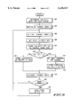
- FIG. 5 is a flowchart illustrating operation of the host processor 102 in a receive mode of operation used to receive and unblock frames of data from the Receive Logic circuit 116.
- the flow starts by waiting until a Frame Sync (FSYNC) 132 signal assertion is received, step 502. This is shown in the flow chart as a loop repeating the test for FSYNC 132 assertion until the signal assertion is received.
- the FSYNC 132 signal assertion, step 502 indicates that a new frame is starting to arrive over the DRX 134 signal line and therefore in a steady operational state a full frame is available in the receive buffer.
- a channel index (“i") is initialized, step 504, and the control word (CW) is read from the serial input, step 506. Then an inner loop is entered, and a codeword of serial input bits is read from the serial input stream into a Data Word (DW i ) corresponding to the channel index ("i"), step 510. A test is then made whether the corresponding valid bit in the control word (V i ) is set, step 512. If the corresponding control word valid bit (V i ) is set, step 512, the corresponding Data Word (DW i ) is stored in a buffer for further processing by the host processor 102, step 514.
- the channel index ("i") is then incremented, step 516, and a is test made as to whether the channel index ("i") is greater than the maximum number ("N") of supported channels, step 518. If the index ("i") is less than or equal to the maximum number ("N") of supported channels, the inner loop is repeated, and the next Data Word (DW i ) is read from the serial input stream, step 510. Otherwise, an outer loop is repeated, starting with the test for assertion of the FSYNC 132 signal, step 502.
- FIG. 6 is a flowchart illustrating operation of the host processor 102 in a transmit mode of operation to block and transmit frames of data words from the serial interface 112 to the transmit logic circuit 114. It starts for each frame by testing to determine which validity bits to set for each of the channels, step 602. This is followed by initializing a channel index ("i"), step 604. A loop is then entered, and the next channel table is selected, step 606. The validity bit for that next channel table is moved from the channel table entry, step 608, and stored in the outgoing control word (CW i ), step 610. A test is then made whether the validity bit (V i ) is set, step 612.
- step 612 If the validity bit (V i ) is set, step 612, the next data codeword for the channel is moved, step 616, into the outgoing frame buffer as the corresponding Data Word (DW i ), step 618. Otherwise, the value stored in the corresponding Data Word (DW i ) is irrelevant, step 614, since it will be ignored when received by the Receive Logic circuit 116. In either case, the channel index ("i") is incremented, 620, and a test is made whether more channels remain to be processed, step 622. As long as more channels remain to be processed, step 622, the loop is repeated, starting with selecting the next channel table, step 602. When no more channels remain to be processed, step 622, the frame buffer is transmitted to the Transmit Logic circuit 114, and the flow is complete until the next output frame is built.
- FIG. 7 is a timing diagram illustrating the operation of the invention.
- the X axis indicates elapsed time. In the example in FIG. 7, four different events are illustrated.
- the bottom two time lines 702, 703 represent data for two different channels or CODECs operating at different rates.
- a first channel (X) 702 is operating at a slightly higher data rate than a second channel (Y) 703.
- the frame rate (FSYNC 132 asserted) is set to the data rate of the higher speed channel (X).
- the top line represents the multiplexed data 701.
- every outgoing frame contains a valid data word (DW X ) for the faster channel.
- FIG. 8 is a timing diagram illustrating the operation of the transmit logic circuit 114 previously depicted in FIG. 4.
- a valid bit pattern of a transmit sequence is depicted with respect to the timing of the serial interface 102.
- the ratio of the CODEC 122 i speed to the frame rate (FSYNC 132) is 2:3. Therefore, the preferred bit pattern is 110, binary.
- each CODEC 122 i is asynchronous with respect to the serial interface 110. Consequently, this bit pattern could effectively be interpreted at the destination CODEC 122 i as 110, 101, or 011.
- the validity bit pattern phase ⁇ 110 ⁇ is correct with respect to the sampling time of the CODEC 122 i .
- This scenario is depicted by the line "VALIDITY GOOD PHASE" 801.
- host processor 102 supplies data codewords to the CODEC 122 i precisely when required.
- the validity bit pattern phase ⁇ 110 ⁇ is shifted in time to ⁇ 101 ⁇ with respect to the sampling time of the CODEC 122 i .
- This scenario is depicted by the line "BAD CASE 1" 802.
- host processor 102 fails to provide a data word when needed.
- the CODEC 122 i "starves" for data in the second frame.
- host processor 102 provides two data codewords before either are need by the CODEC 122 i . This occurs in the fourth and fifth frames.
- This situation is handled through the use of a two entry FIFO i queue 404 i by the transmit logic 114 to provide uninterrupted flow of data to CODEC 122 i .
- the validity bit pattern phase ⁇ 110 ⁇ is shifted in time to ⁇ 011 ⁇ with respect to the sampling time of the CODEC 122 i .
- This scenario is depicted by the line "BAD CASE 2" 803.
- host processor 102 starves the CODEC 122 i in the first frame. Again, host processor 102 provides two data codewords before either are need by the CODEC 122 i . This occurs in the second and third frames. Again, the situation is resolved correctly through the use of a two-entry FIFO 404 i .
- Each CODEC has its own data rate that does not need to be known a priori or ⁇ allocated ⁇ through complex control channel data.
- the data rate of each source/destination can be dynamically changed without disturbing serial interface formatting and the type of processing performed by the host.
- the serial link is compatible with ⁇ any ⁇ standard serial communication port on a standard processor. Alternatively, a parallel port and link may be utilized.
- the serial data format can be readjusted for different codeword sizes (8, 16, 24, or 2 bits per codeword) with minor hardware change.
- the serial link bit clock is adjusted to the highest rate of the two CODECs thus minimizing the processing/buffering required on the host. In an application where CODECs are implemented as oversampling converters, the serial bit clock can be set to the oversampling clock, thus reusing already existing clock generation hardware.
Landscapes
- Engineering & Computer Science (AREA)
- Computer Networks & Wireless Communication (AREA)
- Signal Processing (AREA)
- Communication Control (AREA)
Abstract
Description
Claims (21)
Priority Applications (1)
| Application Number | Priority Date | Filing Date | Title |
|---|---|---|---|
| US08/996,165 US6128317A (en) | 1997-12-22 | 1997-12-22 | Transmitter and receiver supporting differing speed codecs over single links |
Applications Claiming Priority (1)
| Application Number | Priority Date | Filing Date | Title |
|---|---|---|---|
| US08/996,165 US6128317A (en) | 1997-12-22 | 1997-12-22 | Transmitter and receiver supporting differing speed codecs over single links |
Publications (1)
| Publication Number | Publication Date |
|---|---|
| US6128317A true US6128317A (en) | 2000-10-03 |
Family
ID=25542575
Family Applications (1)
| Application Number | Title | Priority Date | Filing Date |
|---|---|---|---|
| US08/996,165 Expired - Lifetime US6128317A (en) | 1997-12-22 | 1997-12-22 | Transmitter and receiver supporting differing speed codecs over single links |
Country Status (1)
| Country | Link |
|---|---|
| US (1) | US6128317A (en) |
Cited By (23)
| Publication number | Priority date | Publication date | Assignee | Title |
|---|---|---|---|---|
| US20020061061A1 (en) * | 1999-02-22 | 2002-05-23 | Young Whu-Ming | DSL link with scaleable performance |
| US20030065846A1 (en) * | 2001-09-28 | 2003-04-03 | Bennett Joseph A. | System and method of determining the source of a codec |
| US6567399B1 (en) * | 1999-05-05 | 2003-05-20 | 3Com Corporation | Hi-fidelity line card |
| US20030128721A1 (en) * | 2002-01-10 | 2003-07-10 | Rupp Michael E. | Programmable frame splitter |
| US6600740B1 (en) * | 1998-10-03 | 2003-07-29 | Ericsson Inc | Voice quality optimization on multi-codec calls |
| US6801541B1 (en) * | 2000-09-29 | 2004-10-05 | Advanced Micro Devices, Inc. | Method and apparatus for data transmission over an AC-97 protocol link |
| US20040233917A1 (en) * | 2003-05-21 | 2004-11-25 | Gabriel Rocas | Bi-directional single wire interface |
| US6904062B1 (en) * | 1999-04-23 | 2005-06-07 | Waytech Investment Co. Ltd. | Method and apparatus for efficient and flexible routing between multiple high bit-width endpoints |
| US20050143843A1 (en) * | 2003-11-25 | 2005-06-30 | Zohar Bogin | Command pacing |
| US20050278168A1 (en) * | 2004-06-14 | 2005-12-15 | Microsoft Corporation | Systems and methods for parsing flexible audio codec topologies |
| US20060031542A1 (en) * | 2004-08-04 | 2006-02-09 | Microsoft Corporation | Equal-opportunity bandwidth regulation |
| US20060034378A1 (en) * | 2002-11-07 | 2006-02-16 | Jan Lindskog | Papr reduction |
| US20060041895A1 (en) * | 2004-08-04 | 2006-02-23 | Microsoft Corporation | Systems and methods for interfacing with codecs across an architecture optimized for audio |
| US20060074637A1 (en) * | 2004-10-01 | 2006-04-06 | Microsoft Corporation | Low latency real-time audio streaming |
| US20060133423A1 (en) * | 2004-12-21 | 2006-06-22 | Casio Computer Co., Ltd. | Data output apparatus, decoding apparatus, and recording medium |
| US20090113092A1 (en) * | 2007-10-25 | 2009-04-30 | Universal Scientific Industrial Co.,Ltd. | Signal converter for debugging that expands fifo capacity |
| US20120017007A1 (en) * | 2002-06-19 | 2012-01-19 | Chapman William L | Robustness improvement for bandwidth communication system |
| US20140063183A1 (en) * | 2012-08-30 | 2014-03-06 | Sung Ho ROH | Method of processing multi-view image and apparatus for executing the same |
| US8889205B2 (en) | 2006-12-27 | 2014-11-18 | Intercontinental Great Brands Llc | Resealable closure with package integrity feature |
| US9663282B2 (en) | 2006-05-23 | 2017-05-30 | International Great Rapids LLC | Package integrity indicator for container closure |
| US9919855B2 (en) | 2007-03-30 | 2018-03-20 | Intercontinental Great Brands Llc | Package integrity indicating closure |
| US11006071B2 (en) * | 2016-02-24 | 2021-05-11 | Iron Bow Technologies, LLC | Integrated telemedicine device |
| US11027892B2 (en) | 2008-07-24 | 2021-06-08 | Deborah Lyzenga | Package integrity indicating closure |
Citations (2)
| Publication number | Priority date | Publication date | Assignee | Title |
|---|---|---|---|---|
| US4813040A (en) * | 1986-10-31 | 1989-03-14 | Futato Steven P | Method and apparatus for transmitting digital data and real-time digitalized voice information over a communications channel |
| US5122875A (en) * | 1991-02-27 | 1992-06-16 | General Electric Company | An HDTV compression system |
-
1997
- 1997-12-22 US US08/996,165 patent/US6128317A/en not_active Expired - Lifetime
Patent Citations (2)
| Publication number | Priority date | Publication date | Assignee | Title |
|---|---|---|---|---|
| US4813040A (en) * | 1986-10-31 | 1989-03-14 | Futato Steven P | Method and apparatus for transmitting digital data and real-time digitalized voice information over a communications channel |
| US5122875A (en) * | 1991-02-27 | 1992-06-16 | General Electric Company | An HDTV compression system |
Cited By (40)
| Publication number | Priority date | Publication date | Assignee | Title |
|---|---|---|---|---|
| US6600740B1 (en) * | 1998-10-03 | 2003-07-29 | Ericsson Inc | Voice quality optimization on multi-codec calls |
| US6804292B2 (en) | 1999-02-22 | 2004-10-12 | Pctel, Inc. | Broadband I/O circuits, interface and bus |
| US20020080869A1 (en) * | 1999-02-22 | 2002-06-27 | Young Whu-Ming | DSL link with embedded control and multi-channel capability |
| US6904083B2 (en) | 1999-02-22 | 2005-06-07 | Pctel, Inc. | DSL link with embedded control and multi-channel capability |
| US6836510B2 (en) | 1999-02-22 | 2004-12-28 | Pctel, Inc. | DSL link with scaleable performance |
| US20020061061A1 (en) * | 1999-02-22 | 2002-05-23 | Young Whu-Ming | DSL link with scaleable performance |
| US6904062B1 (en) * | 1999-04-23 | 2005-06-07 | Waytech Investment Co. Ltd. | Method and apparatus for efficient and flexible routing between multiple high bit-width endpoints |
| US6567399B1 (en) * | 1999-05-05 | 2003-05-20 | 3Com Corporation | Hi-fidelity line card |
| US6801541B1 (en) * | 2000-09-29 | 2004-10-05 | Advanced Micro Devices, Inc. | Method and apparatus for data transmission over an AC-97 protocol link |
| US6820141B2 (en) * | 2001-09-28 | 2004-11-16 | Intel Corporation | System and method of determining the source of a codec |
| US20030065846A1 (en) * | 2001-09-28 | 2003-04-03 | Bennett Joseph A. | System and method of determining the source of a codec |
| US20030128721A1 (en) * | 2002-01-10 | 2003-07-10 | Rupp Michael E. | Programmable frame splitter |
| US6982988B2 (en) * | 2002-01-10 | 2006-01-03 | Intel Corporation | Programmable frame splitter |
| US20120017007A1 (en) * | 2002-06-19 | 2012-01-19 | Chapman William L | Robustness improvement for bandwidth communication system |
| US8855220B2 (en) * | 2002-06-19 | 2014-10-07 | Intellectual Ventures Fund 83 Llc | Robustness improvement for bandwidth communication system |
| US20060034378A1 (en) * | 2002-11-07 | 2006-02-16 | Jan Lindskog | Papr reduction |
| US20040233917A1 (en) * | 2003-05-21 | 2004-11-25 | Gabriel Rocas | Bi-directional single wire interface |
| US7406100B2 (en) | 2003-05-21 | 2008-07-29 | Atmel Corporation | Bi-directional single wire interface |
| US20080279320A1 (en) * | 2003-05-21 | 2008-11-13 | Atmel Corporation | Bi-directional single wire interface |
| US20050143843A1 (en) * | 2003-11-25 | 2005-06-30 | Zohar Bogin | Command pacing |
| US20050278168A1 (en) * | 2004-06-14 | 2005-12-15 | Microsoft Corporation | Systems and methods for parsing flexible audio codec topologies |
| US7756594B2 (en) | 2004-06-14 | 2010-07-13 | Microsoft Corporation | Systems and methods for parsing flexible audio codec topologies |
| US20060041895A1 (en) * | 2004-08-04 | 2006-02-23 | Microsoft Corporation | Systems and methods for interfacing with codecs across an architecture optimized for audio |
| US7590065B2 (en) * | 2004-08-04 | 2009-09-15 | Microsoft Corporation | Equal-opportunity bandwidth regulation |
| US20060031542A1 (en) * | 2004-08-04 | 2006-02-09 | Microsoft Corporation | Equal-opportunity bandwidth regulation |
| US8078302B2 (en) | 2004-10-01 | 2011-12-13 | Microsoft Corporation | Low latency real-time audio streaming |
| US20060074637A1 (en) * | 2004-10-01 | 2006-04-06 | Microsoft Corporation | Low latency real-time audio streaming |
| US20100077110A1 (en) * | 2004-10-01 | 2010-03-25 | Microsoft Corporation | Low Latency Real-Time Audio Streaming |
| US7706901B2 (en) | 2004-10-01 | 2010-04-27 | Microsoft Corporation | Low latency real-time audio streaming |
| US20060133423A1 (en) * | 2004-12-21 | 2006-06-22 | Casio Computer Co., Ltd. | Data output apparatus, decoding apparatus, and recording medium |
| US7630404B2 (en) * | 2004-12-21 | 2009-12-08 | Casio Computer Co., Ltd. | Data output apparatus, decoding apparatus, and recording medium |
| US9663282B2 (en) | 2006-05-23 | 2017-05-30 | International Great Rapids LLC | Package integrity indicator for container closure |
| US8889205B2 (en) | 2006-12-27 | 2014-11-18 | Intercontinental Great Brands Llc | Resealable closure with package integrity feature |
| US9919855B2 (en) | 2007-03-30 | 2018-03-20 | Intercontinental Great Brands Llc | Package integrity indicating closure |
| US10829285B2 (en) | 2007-03-30 | 2020-11-10 | Intercontinental Great Brands Llc | Package integrity indicating closure |
| US20090113092A1 (en) * | 2007-10-25 | 2009-04-30 | Universal Scientific Industrial Co.,Ltd. | Signal converter for debugging that expands fifo capacity |
| US11027892B2 (en) | 2008-07-24 | 2021-06-08 | Deborah Lyzenga | Package integrity indicating closure |
| US20140063183A1 (en) * | 2012-08-30 | 2014-03-06 | Sung Ho ROH | Method of processing multi-view image and apparatus for executing the same |
| CN103686191A (en) * | 2012-08-30 | 2014-03-26 | 三星电子株式会社 | Method of processing multi-view image and apparatus for executing same |
| US11006071B2 (en) * | 2016-02-24 | 2021-05-11 | Iron Bow Technologies, LLC | Integrated telemedicine device |
Similar Documents
| Publication | Publication Date | Title |
|---|---|---|
| US6128317A (en) | Transmitter and receiver supporting differing speed codecs over single links | |
| US5727233A (en) | Byte-mode and burst-mode data transfer mechanism for a high-speed serial interface | |
| JP3819012B2 (en) | Isochronous link protocol | |
| USRE39216E1 (en) | Asynchronous processor access to a switch table in a network with isochronous capability | |
| AU591645B2 (en) | Queueing protocol | |
| KR100283462B1 (en) | Frame-based data transfer | |
| US6687255B1 (en) | Data communication circuit having FIFO buffer with frame-in-FIFO generator | |
| JP3691504B2 (en) | Local loopback of isochronous data in switching mechanisms | |
| US20070160087A1 (en) | Serial media independent interface | |
| JP3465227B2 (en) | Telephone terminal device | |
| US4592050A (en) | Apparatus and method for providing a transparent interface across a satellite communications link | |
| JPH0575594A (en) | Parallel bit synchronizing system | |
| US5164940A (en) | Modular communication system with allocatable bandwidth | |
| US6751232B1 (en) | Method and apparatus for communicating data between first and second pairs of transceivers communicating on a common communications link | |
| JPH10262040A (en) | Synchronization method for data and transmitter and receiver for executing the method | |
| JPS58133066A (en) | Multiplexing method of loop communication system | |
| EP0596650A1 (en) | Apparatus & method for accommodating cable length delays using isochronous fifoing | |
| US5233608A (en) | Method of and a device for receiving data packet form | |
| KR100246773B1 (en) | Apparatus and method for simultaneous transmission of multiple TDM channels | |
| GB2286099A (en) | Modular communication system with allocatable bandwidth | |
| KR100242304B1 (en) | Data transmitting method and apparatus for isdn system | |
| KR100293430B1 (en) | System synchronous clock distribution system of switching equipment | |
| JPH065831B2 (en) | Signal frame transmission method | |
| KR19990055613A (en) | Apparatus and method for simultaneous reception of multiple TDM channels | |
| CA2407966A1 (en) | An apparatus and method for controlling data transmission |
Legal Events
| Date | Code | Title | Description |
|---|---|---|---|
| AS | Assignment |
Owner name: MOTOROLA, INC., ILLINOIS Free format text: ASSIGNMENT OF ASSIGNORS INTEREST;ASSIGNOR:MACKRE, FRANCOIS;REEL/FRAME:008916/0326 Effective date: 19971216 |
|
| STCF | Information on status: patent grant |
Free format text: PATENTED CASE |
|
| FPAY | Fee payment |
Year of fee payment: 4 |
|
| AS | Assignment |
Owner name: FREESCALE SEMICONDUCTOR, INC., TEXAS Free format text: ASSIGNMENT OF ASSIGNORS INTEREST;ASSIGNOR:MOTOROLA, INC.;REEL/FRAME:015698/0657 Effective date: 20040404 Owner name: FREESCALE SEMICONDUCTOR, INC.,TEXAS Free format text: ASSIGNMENT OF ASSIGNORS INTEREST;ASSIGNOR:MOTOROLA, INC.;REEL/FRAME:015698/0657 Effective date: 20040404 |
|
| AS | Assignment |
Owner name: CITIBANK, N.A. AS COLLATERAL AGENT, NEW YORK Free format text: SECURITY AGREEMENT;ASSIGNORS:FREESCALE SEMICONDUCTOR, INC.;FREESCALE ACQUISITION CORPORATION;FREESCALE ACQUISITION HOLDINGS CORP.;AND OTHERS;REEL/FRAME:018855/0129 Effective date: 20061201 Owner name: CITIBANK, N.A. AS COLLATERAL AGENT,NEW YORK Free format text: SECURITY AGREEMENT;ASSIGNORS:FREESCALE SEMICONDUCTOR, INC.;FREESCALE ACQUISITION CORPORATION;FREESCALE ACQUISITION HOLDINGS CORP.;AND OTHERS;REEL/FRAME:018855/0129 Effective date: 20061201 |
|
| FPAY | Fee payment |
Year of fee payment: 8 |
|
| AS | Assignment |
Owner name: CITIBANK, N.A., AS COLLATERAL AGENT,NEW YORK Free format text: SECURITY AGREEMENT;ASSIGNOR:FREESCALE SEMICONDUCTOR, INC.;REEL/FRAME:024397/0001 Effective date: 20100413 Owner name: CITIBANK, N.A., AS COLLATERAL AGENT, NEW YORK Free format text: SECURITY AGREEMENT;ASSIGNOR:FREESCALE SEMICONDUCTOR, INC.;REEL/FRAME:024397/0001 Effective date: 20100413 |
|
| FPAY | Fee payment |
Year of fee payment: 12 |
|
| AS | Assignment |
Owner name: CITIBANK, N.A., AS NOTES COLLATERAL AGENT, NEW YORK Free format text: SECURITY AGREEMENT;ASSIGNOR:FREESCALE SEMICONDUCTOR, INC.;REEL/FRAME:030633/0424 Effective date: 20130521 Owner name: CITIBANK, N.A., AS NOTES COLLATERAL AGENT, NEW YOR Free format text: SECURITY AGREEMENT;ASSIGNOR:FREESCALE SEMICONDUCTOR, INC.;REEL/FRAME:030633/0424 Effective date: 20130521 |
|
| AS | Assignment |
Owner name: ZENITH INVESTMENTS, LLC, DELAWARE Free format text: ASSIGNMENT OF ASSIGNORS INTEREST;ASSIGNOR:FREESCALE SEMICONDUCTOR, INC.;REEL/FRAME:033677/0920 Effective date: 20130627 |
|
| FEPP | Fee payment procedure |
Free format text: PAYOR NUMBER ASSIGNED (ORIGINAL EVENT CODE: ASPN); ENTITY STATUS OF PATENT OWNER: LARGE ENTITY Free format text: PAYER NUMBER DE-ASSIGNED (ORIGINAL EVENT CODE: RMPN); ENTITY STATUS OF PATENT OWNER: LARGE ENTITY |
|
| AS | Assignment |
Owner name: APPLE INC., CALIFORNIA Free format text: ASSIGNMENT OF ASSIGNORS INTEREST;ASSIGNOR:ZENITH INVESTMENTS, LLC;REEL/FRAME:034749/0791 Effective date: 20141219 |
|
| AS | Assignment |
Owner name: FREESCALE SEMICONDUCTOR, INC., TEXAS Free format text: PATENT RELEASE;ASSIGNOR:CITIBANK, N.A., AS COLLATERAL AGENT;REEL/FRAME:037354/0225 Effective date: 20151207 Owner name: FREESCALE SEMICONDUCTOR, INC., TEXAS Free format text: PATENT RELEASE;ASSIGNOR:CITIBANK, N.A., AS COLLATERAL AGENT;REEL/FRAME:037356/0143 Effective date: 20151207 Owner name: FREESCALE SEMICONDUCTOR, INC., TEXAS Free format text: PATENT RELEASE;ASSIGNOR:CITIBANK, N.A., AS COLLATERAL AGENT;REEL/FRAME:037356/0553 Effective date: 20151207 |
|
| AS | Assignment |
Owner name: MORGAN STANLEY SENIOR FUNDING, INC., MARYLAND Free format text: ASSIGNMENT AND ASSUMPTION OF SECURITY INTEREST IN PATENTS;ASSIGNOR:CITIBANK, N.A.;REEL/FRAME:037486/0517 Effective date: 20151207 |
|
| AS | Assignment |
Owner name: NXP, B.V., F/K/A FREESCALE SEMICONDUCTOR, INC., NETHERLANDS Free format text: RELEASE BY SECURED PARTY;ASSIGNOR:MORGAN STANLEY SENIOR FUNDING, INC.;REEL/FRAME:040925/0001 Effective date: 20160912 Owner name: NXP, B.V., F/K/A FREESCALE SEMICONDUCTOR, INC., NE Free format text: RELEASE BY SECURED PARTY;ASSIGNOR:MORGAN STANLEY SENIOR FUNDING, INC.;REEL/FRAME:040925/0001 Effective date: 20160912 |
|
| AS | Assignment |
Owner name: NXP B.V., NETHERLANDS Free format text: RELEASE BY SECURED PARTY;ASSIGNOR:MORGAN STANLEY SENIOR FUNDING, INC.;REEL/FRAME:040928/0001 Effective date: 20160622 |
|
| AS | Assignment |
Owner name: MORGAN STANLEY SENIOR FUNDING, INC., MARYLAND Free format text: CORRECTIVE ASSIGNMENT TO CORRECT THE REMOVE APPLICATION11759915 AND REPLACE IT WITH APPLICATION 11759935 PREVIOUSLY RECORDED ON REEL 037486 FRAME 0517. ASSIGNOR(S) HEREBY CONFIRMS THE ASSIGNMENT AND ASSUMPTION OF SECURITYINTEREST IN PATENTS;ASSIGNOR:CITIBANK, N.A.;REEL/FRAME:053547/0421 Effective date: 20151207 Owner name: MORGAN STANLEY SENIOR FUNDING, INC., MARYLAND Free format text: CORRECTIVE ASSIGNMENT TO CORRECT THE REMOVE APPLICATION 11759915 AND REPLACE IT WITH APPLICATION 11759935 PREVIOUSLY RECORDED ON REEL 037486 FRAME 0517. ASSIGNOR(S) HEREBY CONFIRMS THE ASSIGNMENT AND ASSUMPTION OF SECURITY INTEREST IN PATENTS;ASSIGNOR:CITIBANK, N.A.;REEL/FRAME:053547/0421 Effective date: 20151207 |
|
| AS | Assignment |
Owner name: NXP B.V., NETHERLANDS Free format text: CORRECTIVE ASSIGNMENT TO CORRECT THE REMOVEAPPLICATION 11759915 AND REPLACE IT WITH APPLICATION11759935 PREVIOUSLY RECORDED ON REEL 040928 FRAME 0001. ASSIGNOR(S) HEREBY CONFIRMS THE RELEASE OF SECURITYINTEREST;ASSIGNOR:MORGAN STANLEY SENIOR FUNDING, INC.;REEL/FRAME:052915/0001 Effective date: 20160622 Owner name: NXP B.V., NETHERLANDS Free format text: CORRECTIVE ASSIGNMENT TO CORRECT THE REMOVE APPLICATION 11759915 AND REPLACE IT WITH APPLICATION 11759935 PREVIOUSLY RECORDED ON REEL 040928 FRAME 0001. ASSIGNOR(S) HEREBY CONFIRMS THE RELEASE OF SECURITY INTEREST;ASSIGNOR:MORGAN STANLEY SENIOR FUNDING, INC.;REEL/FRAME:052915/0001 Effective date: 20160622 |
|
| AS | Assignment |
Owner name: NXP, B.V. F/K/A FREESCALE SEMICONDUCTOR, INC., NETHERLANDS Free format text: CORRECTIVE ASSIGNMENT TO CORRECT THE REMOVEAPPLICATION 11759915 AND REPLACE IT WITH APPLICATION11759935 PREVIOUSLY RECORDED ON REEL 040925 FRAME 0001. ASSIGNOR(S) HEREBY CONFIRMS THE RELEASE OF SECURITYINTEREST;ASSIGNOR:MORGAN STANLEY SENIOR FUNDING, INC.;REEL/FRAME:052917/0001 Effective date: 20160912 Owner name: NXP, B.V. F/K/A FREESCALE SEMICONDUCTOR, INC., NETHERLANDS Free format text: CORRECTIVE ASSIGNMENT TO CORRECT THE REMOVE APPLICATION 11759915 AND REPLACE IT WITH APPLICATION 11759935 PREVIOUSLY RECORDED ON REEL 040925 FRAME 0001. ASSIGNOR(S) HEREBY CONFIRMS THE RELEASE OF SECURITY INTEREST;ASSIGNOR:MORGAN STANLEY SENIOR FUNDING, INC.;REEL/FRAME:052917/0001 Effective date: 20160912 |