US6097484A - Location of defects using dye penetration - Google Patents
Location of defects using dye penetration Download PDFInfo
- Publication number
- US6097484A US6097484A US09/353,860 US35386099A US6097484A US 6097484 A US6097484 A US 6097484A US 35386099 A US35386099 A US 35386099A US 6097484 A US6097484 A US 6097484A
- Authority
- US
- United States
- Prior art keywords
- dye
- defects
- top surface
- defect
- gel
- Prior art date
- Legal status (The legal status is an assumption and is not a legal conclusion. Google has not performed a legal analysis and makes no representation as to the accuracy of the status listed.)
- Expired - Lifetime
Links
Images


Classifications
-
- G—PHYSICS
- G01—MEASURING; TESTING
- G01N—INVESTIGATING OR ANALYSING MATERIALS BY DETERMINING THEIR CHEMICAL OR PHYSICAL PROPERTIES
- G01N21/00—Investigating or analysing materials by the use of optical means, i.e. using sub-millimetre waves, infrared, visible or ultraviolet light
- G01N21/84—Systems specially adapted for particular applications
- G01N21/88—Investigating the presence of flaws or contamination
- G01N21/91—Investigating the presence of flaws or contamination using penetration of dyes, e.g. fluorescent ink
-
- G—PHYSICS
- G01—MEASURING; TESTING
- G01N—INVESTIGATING OR ANALYSING MATERIALS BY DETERMINING THEIR CHEMICAL OR PHYSICAL PROPERTIES
- G01N21/00—Investigating or analysing materials by the use of optical means, i.e. using sub-millimetre waves, infrared, visible or ultraviolet light
- G01N21/84—Systems specially adapted for particular applications
- G01N21/88—Investigating the presence of flaws or contamination
- G01N21/95—Investigating the presence of flaws or contamination characterised by the material or shape of the object to be examined
- G01N21/9501—Semiconductor wafers
Definitions
- This invention relates to locating defects during semiconductor manufacturing. More specifically, the invention relates to a method and device for finding surface and subsurface defects on wafers using dye to amplify the size of the defects.
- a defect in a wafer if uncorrected, can cause the failure of the final product, an integrated circuit (IC) chip. Identifying the defect during processing is particularly valuable for several reasons. For example, if the defects were discovered during one step of the processing, it is possible that the wafer could be reworked to eliminate the defect(s). Additionally, even if the wafer could not be reworked, identifying the location and frequency of the defects will provide important information regarding the repeatability and quality of the previous processes. This information can then be used to makes changes to the previous processes so as to minimize the defects.
- CMP chemical metal planarization
- a particularly serious defect is an embedded particle in an oxide that the CMP process rips out thereby leaving a void in the oxide. This void could subsequently be filled with tungsten or another metal and not removed by a later CMP process. This puddle of metal could then result in a die-killing short circuit at subsequent metal levels.
- Unfilled vias have many causes including the metal being pulled out during the CMP process or the filling of the via may have been blocked by a particle. Deviations in the via top profile can be caused due to local arcing or cratering.
- the typical procedure is to inspect the wafer for defects with an optical comparitor tool. Once the locations of defects are determined, the locations are given to another tool, which will characterize the defect.
- Two such tools used for characterization of defects are an optical inspection tool or a scanning electron microscope (SEM).
- SEM scanning electron microscope
- the advantage of using an optical inspection tool is its ability to position itself to the defect and quickly focus on the defect.
- an optical inspection tool has difficulty distinguishing between a surface defect and a void at high magnification levels of approximately 0.25 micros per pixel. As the features become smaller than 0.25 microns, the wavelength of the light reflected from defects of similar size is not long enough for the optical inspection tool to characterize the defect.
- the defects can be characterized using a SEM.
- use of a SEM presents different problems.
- a SEM cannot easily focus on a substantially flat oxide film.
- throughput (i.e., the number of inspections during a given period of time) of an SEM is much smaller than the throughput of an optical inspection tool. With the throughput of an SEM being so low, the use of a SEM during manufacturing is typically considered not feasible.
- the current devices and methods of detecting these defects are inadequate.
- noise Another problem associate with current inspection methods are their vulnerability to "noise".
- One type of noise that affects current inspection methods is from the underlying metal pattern or from the metal grain in the situation of large metal areas.
- Another type of noise is color noise originating from the variation of oxide film thickness across the wafer and from die to die.
- It is still another object of the invention is to provide a method and device for detecting surface and subsurface defects which are not susceptible to noise caused by the underlying metal pattern or from the metal grain or color noise originating from the variation of oxide film thickness across the wafer and from die to die.
- the subject method comprises the steps of applying a dye, removing the dye, and applying a developing gel.
- the dye Upon application of the dye, the dye enters defects connected to the top surface of the semiconductor device.
- the dye contained within the defects leaches into the developing gel to form defect indications. These defect indications have a better optical visibility than the defects themselves.
- a second embodiment of the invention is an defect amplifier which comprises a dye applicator, a dye remover, and a gel applicator.
- the dye applicator applies a layer of dye to a top surface of the semiconductor device. Upon application of the dye onto the top surface, the dye enters into the defects. The dye remover removes the remaining dye from the top surface.
- the gel applicator then applies a layer of developing gel to the top surface. The dye then leaches from the defects into the developing gel to form defect indications.
- a heater can be provided to heat the developing gel so as to increase the leaching rate of the dye into the developing gel.
- an optical reader can be provided for reading the defect indications.
- both the dye applicator and gel applicator are spin coaters.
- FIGS. 1 through 5 are side cross-sectional views illustrating one sequence of steps involved in the method of detecting surface and subsurface defects on a semiconductor wafer.
- FIG. 1 shows a layer having defects such as a crack, partial void, and void.
- FIG. 2 shows the layer of FIG. 1 after the application of dye onto the top surface of the layer.
- FIG. 3 shows the layer of FIG. 2 after the dye has been removed from the top surface of the layer.
- FIG. 4 shows the layer of FIG. 3 after a developing gel has been applied to the top surface of the layer.
- FIG. 5 shows the layer of FIG. 4 after the dye has been leached into the developing gel.
- FIG. 6 shows a top plan view of FIG. 5 illustrating the different patterns exhibited by different types of defect indications.
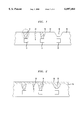
- FIG. 7 is a perspective view of a defect amplifier for amplifying defects on a semiconductor device according to an embodiment of the invention.
- FIG. 8 is a side view of the defect amplifier as illustrated in FIG. 7.
- FIG. 1 illustrates a layer 10 of a semiconductor wafer to be examined.
- Layers 10 of semiconductor wafers can be formed from many different materials, and this invention is not limited as to be used with a particular type of material.
- a typical material used for a layer 10 is an oxide, for example, a silicon oxide.
- a partial void 16 can be created by many reasons, for example, the window 14 may not have been completely filled during deposition or the CMP process may have pulled out a portion of the window 14.
- a void 18 can be the result of incomplete filling of the window 14 or the pulling out of a portion of the window 14. However, the void 18 does not necessarily have to be associated with a window 14. The void 18 can be created anywhere along the top surface 20 of the layer 10.
- Still another type of defect associated with semiconductor manufacturing is a crack 22.
- Other types of surface and subsurface defects are also well known in semiconductor manufacturing. The aforementioned defects are only intended to be illustrative of the types of defects present during semiconductor manufacturing and are not intended to limit the present invention in any manner.
- FIG. 2 illustrates the application of the penetrant dye 24 onto the top surface 20 of the layer 10.
- the penetrant dye 24 acts to penetrate into defects, such as cavities or recesses, connected to the top surface 20. Examples of these cavities or recesses are cracks 22, partial voids 16, and voids 18. It being understood that the penetrant dye 24 is not limited to penetration into cracks 22, partial voids 16, and voids 18, but will penetrate into any cavity or recess connected to the top surface 20.
- Penetrant dyes 24 are known in the art, and this invention is not limited as to a particular type of penetrant dye 24. Penetrant dyes 24 can have many different qualities, for example, the penetrant dye 24 can be fluorescent to aid in the detection of a defect. Also, the penetrant dye 24 can be optically reflective at different wavelengths of light.
- any method or device of applying the penetrant dye 24 to the top surface 20 of the layer 10 is acceptable so long as the penetrant dye 24 completely covers the surface area to be examined.
- the presently preferred device for applying the penetrant dye 24 to the top surface 20 is a spin coater.
- a spin coater is known in the art and is used with other semiconductor manufacturing processes to apply an uniform film of liquid to the top surface 20 of a wafer.
- FIG. 3 illustrates the layer 10 after the penetrant dye 24 disposed on the top surface 20 of the layer 10 has been removed. It is noted that the penetrant dye 24, although removed from the top surface 20, still remains in any cavities or recesses connected to the top surface 20, for examples cracks 22, partial voids 16, and voids 18. The penetrant dye 24 can remain in the cavities and recesses by surface tension, for example.
- the method or device used to remove the penetrant dye 24 from the top surface 20 of the layer 10 preferably does not remove the penetrant dye 24 from the cavities or recesses.
- Such methods or devices are commonly known, and all so capable are acceptable for use with the present invention.
- FIG. 4 illustrates the layer 10 after a developing gel 26 has been applied to the top surface 20.
- the function of the developing gel 26 is to absorb the penetrant dye 24 contained with the cavities or recesses.
- Many types of developing gels 26 are known in the art, and any developing gel 26 capable of absorbing the penetrant dye 24 is acceptable for use with the present invention.
- penetrant dye systems typically include both a penetrant dye 24 and a developing gel 26 with the developing gel 26 specifically tailored to be used with the penetrant dye 24. As such, selection of both the penetrant dye 24 and developing gel 26 will preferably be done in combination.
- penetrant dye system One presently preferred characteristic of the penetrant dye system is that a bright contrast exists between the developing gel 26 and the developing gel 26 after absorption of penetrant dye 24. This bright contrast allows for better optical identification of those defect indications 38 in which the developing gel 26 has absorbed the penetrant dye 24. Also, a penetrant dye system can be selected so that application of heat to the developing gel 26 can increase the diffusion rate of the penetrant dye 24 into the developing gel 26. Advantageously, this characteristic allows for quicker optical identification of the defects after the developing gel 26 has been applied to the top surface 26.
- any method or device of applying the developing gel 26 to the top surface 20 of the layer 10 is acceptable so long as the developing gel 26 completely covers the surface area to be examined.
- the presently preferred device for applying the developing dye 26 to the top surface 20 is a spin coater.
- FIG. 6 illustrates various defect indications 38 in the developing gel.
- a defect indication 38 is the dye stain related to defect.
- Each type of defect will have a characteristic defect indication pattern and size.
- a crack can be indicated a line 28 having a length significantly greater than its width.
- a large defect such as a void, can be indicated by a substantial circular large mark 30, and a partial void can be indicated by a smaller mark 32. It should be noted that other defects may exhibit other characteristic defect indication patterns and sizes, and this invention is not limited as to indicating a particular type, pattern, or size of defect.
- the defect amplifier 40 comprises a dye applicator 42, a dye remover 44, a gel applicator 46, a heater 48, and an optical reader 50.
- the optical reader 50 can be separate from the defect amplifier 40.
- the dye applicator 42 acts to apply a layer of penetrant dye over those areas of the wafer to be inspected.
- any dye applicator 42 capable of applying a layer of penetrant dye onto the wafer to be inspected is acceptable for use in the present invention.
- the presently preferred dye applicator 42 is a spin coater.
- a spin coater advantageously is already being used in the processing of semiconductor wafers and is capable of applying a thin, constant-thickness layer of fluid onto the surface of a wafer.
- the dye remover 44 acts to remove the penetrant dye from the surface of the wafer without removing the penetrant dye contained with the cavities or recesses connected to the surface.
- any dye remover 44 capable of removing the penetrant dye from the surface of the wafer without removing the penetrant dye contained with the cavities or recesses connected to the surface is acceptable for use in the present invention.
- the presently preferred dye applicator 42 is a bladed squeegee.
- the gel applicator 46 acts to apply a layer of developing gel over those areas of the wafer to be inspected.
- any gel applicator 46 capable of applying a layer of developing gel onto the wafer to be inspected is acceptable for use in the present invention.
- the presently preferred gel applicator 46 is a spin coater.
- the spin coater is used to apply a thin, constant-thickness layer of developing gel onto the surface of a wafer.
- the spin coater used for the dye applicator 42 is the same spin coater used for the gel applicator 46.
- a heater 48 can optionally be provided to increase the diffusion rate of the penetrant dye into the developing gel as previously discussed. Heaters 48 are well known in the art and any heater capable of providing a desired amount of heat to the developing gel is acceptable for use with the present invention.
- the optical reader 50 is used to identify and characterize the defects revealed by the defect indications on the developing gel.
- Optical readers 50 are well known in the art, and this invention is not limited as to a particular optical reader 50.
- the optical reader 50 can be integral with the defect amplifier 40.
- the optical reader 50 can be separate for the defect amplifier 40 with the wafer being subsequently moved from the defect amplifier 40 to the optical reader 50 after the defect amplifier 40 has amplified the defects on the wafer.
Abstract
Description
Claims (14)
Priority Applications (1)
| Application Number | Priority Date | Filing Date | Title |
|---|---|---|---|
| US09/353,860 US6097484A (en) | 1999-07-15 | 1999-07-15 | Location of defects using dye penetration |
Applications Claiming Priority (1)
| Application Number | Priority Date | Filing Date | Title |
|---|---|---|---|
| US09/353,860 US6097484A (en) | 1999-07-15 | 1999-07-15 | Location of defects using dye penetration |
Publications (1)
| Publication Number | Publication Date |
|---|---|
| US6097484A true US6097484A (en) | 2000-08-01 |
Family
ID=23390901
Family Applications (1)
| Application Number | Title | Priority Date | Filing Date |
|---|---|---|---|
| US09/353,860 Expired - Lifetime US6097484A (en) | 1999-07-15 | 1999-07-15 | Location of defects using dye penetration |
Country Status (1)
| Country | Link |
|---|---|
| US (1) | US6097484A (en) |
Cited By (10)
| Publication number | Priority date | Publication date | Assignee | Title |
|---|---|---|---|---|
| US6174727B1 (en) * | 1998-11-03 | 2001-01-16 | Komatsu Electronic Metals, Co. | Method of detecting microscopic defects existing on a silicon wafer |
| US6383816B1 (en) * | 1998-11-10 | 2002-05-07 | University Of Delaware | Probing of surface roughness |
| US20030180966A1 (en) * | 2002-03-20 | 2003-09-25 | Wisconsin Alumni Research Foundation | Optical imaging of nanostructured substrates |
| US20050079487A1 (en) * | 2003-07-17 | 2005-04-14 | Wisconsin Alumni Research Foundation | Liquid crystals with reduced toxicity and applications thereof |
| US20070097360A1 (en) * | 2005-10-28 | 2007-05-03 | Turbomeca | Diagnosing or determining parameters for an installation for detecting open defects in the surfaces of parts by sweating |
| US20070231832A1 (en) * | 2005-10-31 | 2007-10-04 | Wisconsin Alumni Research Foundation | Device and methods for liquid crystal-based bioagent detection |
| US20090180587A1 (en) * | 2008-01-10 | 2009-07-16 | Sang Hee Nam | Method of detecting fine surface defects |
| US20100291685A1 (en) * | 2007-12-17 | 2010-11-18 | Life Technologies Corporation | Methods for detecting defects in inorganic-coated polymer surfaces |
| US8605276B2 (en) * | 2011-11-01 | 2013-12-10 | Taiwan Semiconductor Manufacturing Company, Ltd. | Enhanced defect scanning |
| US9310315B2 (en) | 2007-12-17 | 2016-04-12 | Life Technologies Corporation | Methods for detecting defects in inorganic-coated polymer surfaces |
Citations (1)
| Publication number | Priority date | Publication date | Assignee | Title |
|---|---|---|---|---|
| US5965446A (en) * | 1996-10-24 | 1999-10-12 | Hamamatsu Photonics K.K. | Method for placing fluorescent single molecules on surface of substrate and method for visualizing structural defect of surface of substrate |
-
1999
- 1999-07-15 US US09/353,860 patent/US6097484A/en not_active Expired - Lifetime
Patent Citations (1)
| Publication number | Priority date | Publication date | Assignee | Title |
|---|---|---|---|---|
| US5965446A (en) * | 1996-10-24 | 1999-10-12 | Hamamatsu Photonics K.K. | Method for placing fluorescent single molecules on surface of substrate and method for visualizing structural defect of surface of substrate |
Cited By (20)
| Publication number | Priority date | Publication date | Assignee | Title |
|---|---|---|---|---|
| US6174727B1 (en) * | 1998-11-03 | 2001-01-16 | Komatsu Electronic Metals, Co. | Method of detecting microscopic defects existing on a silicon wafer |
| US6383816B1 (en) * | 1998-11-10 | 2002-05-07 | University Of Delaware | Probing of surface roughness |
| US20030180966A1 (en) * | 2002-03-20 | 2003-09-25 | Wisconsin Alumni Research Foundation | Optical imaging of nanostructured substrates |
| WO2003081230A1 (en) * | 2002-03-20 | 2003-10-02 | Wisconsin Alumni Research Foundation | Optical imaging of nanostructured substrates |
| US7807348B2 (en) | 2002-03-20 | 2010-10-05 | Wisconsin Alumni Research Foundation | Optical imaging of nanostructured substrates |
| US20050079487A1 (en) * | 2003-07-17 | 2005-04-14 | Wisconsin Alumni Research Foundation | Liquid crystals with reduced toxicity and applications thereof |
| US7951577B2 (en) | 2003-07-17 | 2011-05-31 | Wisconsin Alumni Research Foundation | Liquid crystals with reduced toxicity and applications thereof |
| US7303694B2 (en) | 2003-07-17 | 2007-12-04 | Wisconsin Alumni Research Foundation | Liquid crystals with reduced toxicity and applications thereof |
| US20080050799A1 (en) * | 2003-07-17 | 2008-02-28 | Wisconsin Alumni Research Foundation | Liquid crystals with reduced toxicity and applications thereof |
| US7746458B2 (en) * | 2005-10-28 | 2010-06-29 | Turbomeca | Diagnosing or determining parameters for an installation for detecting open defects in the surfaces of parts by sweating |
| US20070097360A1 (en) * | 2005-10-28 | 2007-05-03 | Turbomeca | Diagnosing or determining parameters for an installation for detecting open defects in the surfaces of parts by sweating |
| US20070231832A1 (en) * | 2005-10-31 | 2007-10-04 | Wisconsin Alumni Research Foundation | Device and methods for liquid crystal-based bioagent detection |
| US7910382B2 (en) | 2005-10-31 | 2011-03-22 | Wisconsin Alumni Research Foundation | Device and methods for liquid crystal-based bioagent detection |
| US20110183357A1 (en) * | 2005-10-31 | 2011-07-28 | Wisconsin Alumni Research Foundation | Device and methods for liquid crystal-based bioagent detection |
| US8329423B2 (en) | 2005-10-31 | 2012-12-11 | Wisconsin Alumni Research Foundation | Device and methods for liquid crystal-based bioagent detection |
| US20100291685A1 (en) * | 2007-12-17 | 2010-11-18 | Life Technologies Corporation | Methods for detecting defects in inorganic-coated polymer surfaces |
| US8304242B2 (en) * | 2007-12-17 | 2012-11-06 | Life Technologies Corporation | Methods for detecting defects in inorganic-coated polymer surfaces |
| US9310315B2 (en) | 2007-12-17 | 2016-04-12 | Life Technologies Corporation | Methods for detecting defects in inorganic-coated polymer surfaces |
| US20090180587A1 (en) * | 2008-01-10 | 2009-07-16 | Sang Hee Nam | Method of detecting fine surface defects |
| US8605276B2 (en) * | 2011-11-01 | 2013-12-10 | Taiwan Semiconductor Manufacturing Company, Ltd. | Enhanced defect scanning |
Similar Documents
| Publication | Publication Date | Title |
|---|---|---|
| US6330354B1 (en) | Method of analyzing visual inspection image data to find defects on a device | |
| US6097484A (en) | Location of defects using dye penetration | |
| JPH11307604A (en) | Process monitoring method and device | |
| CN104008956A (en) | Unsealing method for flip chip device | |
| KR100629921B1 (en) | Test handler and method for test of semiconductor package | |
| CN104851820A (en) | Semiconductor device defect detection method | |
| US20080318343A1 (en) | Wafer reclaim method based on wafer type | |
| US7330042B2 (en) | Substrate inspection system, substrate inspection method, and substrate inspection apparatus | |
| JP2006191101A (en) | Device and method for inspecting metal residues | |
| JP2002026096A (en) | Method for evaluating quality of silicon wafer and method for regenerating silicon wafer | |
| JP3737585B2 (en) | Semiconductor wafer surface inspection method and semiconductor device manufacturing apparatus | |
| JP5622338B2 (en) | Method for discriminating and checking foreign matter and scratch marks in semiconductor device manufacturing process | |
| CN110618004B (en) | Improved back unsealing method of semiconductor device | |
| US7268574B2 (en) | Systems and methods for sensing obstructions associated with electrical testing of microfeature workpieces | |
| KR100694597B1 (en) | Method for inspecting a defect of pattern in semiconductor device | |
| JP2018146531A (en) | Substrate inspection device, substrate polishing device, substrate inspection method, and substrate polishing method | |
| US6853873B1 (en) | Enhanced throughput of a metrology tool | |
| JP3903901B2 (en) | Thin film device thickness inspection method | |
| JP2008251975A (en) | Visual inspection method for object being inspected, and equipment provided with the same | |
| Lewis | Infrared Microscopy as applied to failure analysis of P-DIP Devices | |
| TWI737548B (en) | Method for manufacturing a sample for observing failure areas in failure analysis | |
| US6291833B2 (en) | Apparatus for mapping scratches in an oxide film | |
| KR200368650Y1 (en) | Test handler for test of semiconductor package | |
| US6611326B1 (en) | System and apparatus for evaluating the effectiveness of wafer drying operations | |
| JPH11274254A (en) | Device and method for checking appearance |
Legal Events
| Date | Code | Title | Description |
|---|---|---|---|
| AS | Assignment |
Owner name: LUCENT TECHNOLOGIES INC., NEW JERSEY Free format text: ASSIGNMENT OF ASSIGNORS INTEREST;ASSIGNORS:MCINTOSH, JOHN M.;KANE, BRITTIN C.;CREVASSE, ANNETTE M.;AND OTHERS;REEL/FRAME:010107/0432;SIGNING DATES FROM 19990706 TO 19990707 |
|
| STCF | Information on status: patent grant |
Free format text: PATENTED CASE |
|
| FPAY | Fee payment |
Year of fee payment: 4 |
|
| FPAY | Fee payment |
Year of fee payment: 8 |
|
| FPAY | Fee payment |
Year of fee payment: 12 |
|
| AS | Assignment |
Owner name: DEUTSCHE BANK AG NEW YORK BRANCH, AS COLLATERAL AG Free format text: PATENT SECURITY AGREEMENT;ASSIGNORS:LSI CORPORATION;AGERE SYSTEMS LLC;REEL/FRAME:032856/0031 Effective date: 20140506 |
|
| AS | Assignment |
Owner name: AVAGO TECHNOLOGIES GENERAL IP (SINGAPORE) PTE. LTD Free format text: ASSIGNMENT OF ASSIGNORS INTEREST;ASSIGNOR:AGERE SYSTEMS LLC;REEL/FRAME:035365/0634 Effective date: 20140804 |
|
| AS | Assignment |
Owner name: AGERE SYSTEMS LLC, PENNSYLVANIA Free format text: TERMINATION AND RELEASE OF SECURITY INTEREST IN PATENT RIGHTS (RELEASES RF 032856-0031);ASSIGNOR:DEUTSCHE BANK AG NEW YORK BRANCH, AS COLLATERAL AGENT;REEL/FRAME:037684/0039 Effective date: 20160201 Owner name: LSI CORPORATION, CALIFORNIA Free format text: TERMINATION AND RELEASE OF SECURITY INTEREST IN PATENT RIGHTS (RELEASES RF 032856-0031);ASSIGNOR:DEUTSCHE BANK AG NEW YORK BRANCH, AS COLLATERAL AGENT;REEL/FRAME:037684/0039 Effective date: 20160201 |
|
| AS | Assignment |
Owner name: BANK OF AMERICA, N.A., AS COLLATERAL AGENT, NORTH CAROLINA Free format text: PATENT SECURITY AGREEMENT;ASSIGNOR:AVAGO TECHNOLOGIES GENERAL IP (SINGAPORE) PTE. LTD.;REEL/FRAME:037808/0001 Effective date: 20160201 Owner name: BANK OF AMERICA, N.A., AS COLLATERAL AGENT, NORTH Free format text: PATENT SECURITY AGREEMENT;ASSIGNOR:AVAGO TECHNOLOGIES GENERAL IP (SINGAPORE) PTE. LTD.;REEL/FRAME:037808/0001 Effective date: 20160201 |
|
| AS | Assignment |
Owner name: AVAGO TECHNOLOGIES GENERAL IP (SINGAPORE) PTE. LTD., SINGAPORE Free format text: TERMINATION AND RELEASE OF SECURITY INTEREST IN PATENTS;ASSIGNOR:BANK OF AMERICA, N.A., AS COLLATERAL AGENT;REEL/FRAME:041710/0001 Effective date: 20170119 Owner name: AVAGO TECHNOLOGIES GENERAL IP (SINGAPORE) PTE. LTD Free format text: TERMINATION AND RELEASE OF SECURITY INTEREST IN PATENTS;ASSIGNOR:BANK OF AMERICA, N.A., AS COLLATERAL AGENT;REEL/FRAME:041710/0001 Effective date: 20170119 |
|
| AS | Assignment |
Owner name: BELL SEMICONDUCTOR, LLC, ILLINOIS Free format text: ASSIGNMENT OF ASSIGNORS INTEREST;ASSIGNORS:AVAGO TECHNOLOGIES GENERAL IP (SINGAPORE) PTE. LTD.;BROADCOM CORPORATION;REEL/FRAME:044886/0608 Effective date: 20171208 |
|
| AS | Assignment |
Owner name: CORTLAND CAPITAL MARKET SERVICES LLC, AS COLLATERA Free format text: SECURITY INTEREST;ASSIGNORS:HILCO PATENT ACQUISITION 56, LLC;BELL SEMICONDUCTOR, LLC;BELL NORTHERN RESEARCH, LLC;REEL/FRAME:045216/0020 Effective date: 20180124 |
|
| AS | Assignment |
Owner name: BELL NORTHERN RESEARCH, LLC, ILLINOIS Free format text: RELEASE BY SECURED PARTY;ASSIGNOR:CORTLAND CAPITAL MARKET SERVICES LLC;REEL/FRAME:059720/0719 Effective date: 20220401 Owner name: BELL SEMICONDUCTOR, LLC, ILLINOIS Free format text: RELEASE BY SECURED PARTY;ASSIGNOR:CORTLAND CAPITAL MARKET SERVICES LLC;REEL/FRAME:059720/0719 Effective date: 20220401 Owner name: HILCO PATENT ACQUISITION 56, LLC, ILLINOIS Free format text: RELEASE BY SECURED PARTY;ASSIGNOR:CORTLAND CAPITAL MARKET SERVICES LLC;REEL/FRAME:059720/0719 Effective date: 20220401 |