US6085258A - State machine for selectively performing an operation on a single or a plurality of registers depending upon the register address specified in a packet - Google Patents
State machine for selectively performing an operation on a single or a plurality of registers depending upon the register address specified in a packet Download PDFInfo
- Publication number
- US6085258A US6085258A US09/100,270 US10027098A US6085258A US 6085258 A US6085258 A US 6085258A US 10027098 A US10027098 A US 10027098A US 6085258 A US6085258 A US 6085258A
- Authority
- US
- United States
- Prior art keywords
- register
- registers
- read
- access
- state machine
- Prior art date
- Legal status (The legal status is an assumption and is not a legal conclusion. Google has not performed a legal analysis and makes no representation as to the accuracy of the status listed.)
- Expired - Lifetime
Links
Images


Classifications
-
- G—PHYSICS
- G06—COMPUTING; CALCULATING OR COUNTING
- G06F—ELECTRIC DIGITAL DATA PROCESSING
- G06F13/00—Interconnection of, or transfer of information or other signals between, memories, input/output devices or central processing units
- G06F13/10—Program control for peripheral devices
- G06F13/12—Program control for peripheral devices using hardware independent of the central processor, e.g. channel or peripheral processor
- G06F13/124—Program control for peripheral devices using hardware independent of the central processor, e.g. channel or peripheral processor where hardware is a sequential transfer control unit, e.g. microprocessor, peripheral processor or state-machine
- G06F13/128—Program control for peripheral devices using hardware independent of the central processor, e.g. channel or peripheral processor where hardware is a sequential transfer control unit, e.g. microprocessor, peripheral processor or state-machine for dedicated transfers to a network
-
- H—ELECTRICITY
- H04—ELECTRIC COMMUNICATION TECHNIQUE
- H04L—TRANSMISSION OF DIGITAL INFORMATION, e.g. TELEGRAPHIC COMMUNICATION
- H04L69/00—Network arrangements, protocols or services independent of the application payload and not provided for in the other groups of this subclass
- H04L69/30—Definitions, standards or architectural aspects of layered protocol stacks
- H04L69/32—Architecture of open systems interconnection [OSI] 7-layer type protocol stacks, e.g. the interfaces between the data link level and the physical level
- H04L69/322—Intralayer communication protocols among peer entities or protocol data unit [PDU] definitions
- H04L69/323—Intralayer communication protocols among peer entities or protocol data unit [PDU] definitions in the physical layer [OSI layer 1]
Definitions
- This invention relates to the field of data communications. More specifically, it relates to the field of serial port access to registers and to the field of serial port access to multiple registers.
- a device may contain a plurality of registers which communicate with a serial port from which data is written into the registers and to which data is read from the registers.
- a system may include a plurality of such devices each having its own plurality of registers.
- IEEE Standard 802.3u defines the logical, electrical, and mechanical characteristics for the Reconciliation sublayer and Media Independent Interface (MII) between CSMA/CD media access controllers and various physical layer devices.
- MII Media Independent Interface
- the physical layer devices in this system may have a management port which is a register-based serial port. During system operation, data may be written to and read from individual ones of the registers in the physical devices.
- a packet of information asserted on the serial port contains a read/write operation identifier, an address of the physical device containing the register of interest, an address of the register of interest within that device, and, if the operation is a write operation, the data to be written into the register.
- the packet also contains bits used to synchronize the receipt of the information contained therein.
- a multiple-register-access-capable device includes a plurality of registers and a serial port with which the plurality of registers communicate. Communications packets arriving on the serial port include information identifying the device and register within the device for which they are destined. Packets either contain data to be written into the destination register or contain data that are to be written out to the serial port.
- the multiple-register-access-capable device of the present invention is equipped with the capability to turn the multiple register access mode on and off. This allows the multiple-register-access-capable device of the present invention to be used in systems which do not support multiple register access.
- the multiple register access mode is turned on before multiple register access is attempted.
- the multiple-register-access-capable device of the present invention includes a serial port coupled to a plurality of registers.
- the multiple-register-access-capable device of the present invention is controlled by a state machine or some equivalent logic block.
- Information written into the multiple-register-access-capable device of the present invention (usually a single bit in one of the registers, a pin on the integrated circuit, etc.) identifies whether the multiple-register-access-capable device of the present invention is in a single-register or multiple-register mode.
- the state machine which controls the device operates in a single-register mode if the bit is disabled and operates in a multiple-register mode if the bit is enabled.
- the multiple-register-access-capable device of the present invention operates in a manner known in the prior art whereby a single register is identified for reading or writing and data are then either written into the register or read out from the register in response to a write or read request.
- data are written into or read out from all registers or from a group of registers in the device in response to the write or read request.
- a read or write operation addressed to a selected register is interpreted as a request to read or write from all registers in a defined group of registers and the state machine directs the operation of the device to accomplish a read from or write to all of the registers in the group.
- the multiple-register-access-capable device of the present invention is in single-register mode, operations addressed to the selected register cause normal read or write operation to be executed with respect to that register.
- a multiple-register-access-capable device of the present invention may be in single-register access mode or in multiple-register access mode.
- single-register access mode the device is compatible with prior-art devices and operates in the manner known in the prior art for single-register read and write operations.
- placing the multiple-register-access-capable device of the present invention into single-register or multiple-register mode may be accomplished by setting or resetting a multiple-register-access bit which occupies a selected bit position in one of the registers in the device.
- the state machine controlling the operation of the device When in single-register access mode, the state machine controlling the operation of the device is caused to operate the device in the manner well known in the prior art. When in multiple-register access mode, the state machine controlling the operation of the device is caused to operate the device in the manner well known in the prior art unless a selected register is addressed for a read or write operation. When the selected register is addressed, the state machine causes the device to perform the requested read or write operation on a plurality of registers, usually all of the registers in the device.
- a write frame asserted at the serial port of the device addressed to the selected register will have a data field comprising all of the data to be written into all of the plurality of registers.
- a read frame asserted at the serial port of the device addressed to the selected register will cause all of the plurality of registers to drive their contents onto the serial port.
- one or more driving devices are connected to a serial bus.
- One or more multiple-register-access-capable devices disclosed herein are also connected to the serial bus.
- FIG. 1 is a block diagram of a system including a plurality of register-based serial port devices connected to a serial port.
- FIG. 2 is a bit map of typical read and write packets addressed to a device such as one of the ones shown in FIG. 1.
- FIG. 3 is a block diagram of a multiple-register-access-capable device according to the present invention connected to a serial port.
- FIG. 4 is a bit map of typical read and write packets addressed to a device such as the one in FIG. 3.
- FIG. 5 is a block diagram of a system including a plurality of register-based serial port devices in accordance with the present invention connected to a serial port.
- FIG. 6 is a flow diagram illustrating a presently preferred embodiment of the method of the present invention.
- IEEE Standard 802.3u, clause 22 defines the logical, electrical, and mechanical characteristics for the Reconciliation sublayer and Media Independent Interface between CSMA/CD media access controllers and various physical layer devices.
- the purpose of the MII is to provide a simple, inexpensive, and easily implemented interconnection between the Media Access Control sublayer and Physical layer devices, and between Physical layer devices and Station Management entities.
- the MII is a nibble interface between the controller and a Physical Device.
- the MI is a serial management interface between a physical device and some management station.
- FIG. 1 a block diagram shows a generic representation of a relevant portion of a prior-art communications arrangement 10 (such as one which operates according to IEEE standard 802.3u) including a controller 12 communicating with a serial link 14.
- Controller 12 may be any of a number of known devices such as ethernet controllers, microcontrollers, Application Specific Integrated Circuits (ASICs), or any other logic device for system management.
- a plurality of register-based serial port devices 16a through 16c (referred to as "Physical Devices" in the IEEE protocol) are also shown in communication with the bus 14.
- FIG. 1 illustrates a typical environment in which the present invention can be employed.
- the serial link 14 that is connected between controller 12 and serial port devices 16a through 16c provides the communications link between those devices.
- the IEEE standard referenced above provides a simple, two wire, serial interface to connect a management entity and a managed Physical Device like the register-based serial port devices of FIG. 1 for purposes of controlling the Physical Devices and gathering status from the Physical Devices.
- This management interface is the MI serial link referred to above.
- the two signals that make up the Management Interface are the management data clock (MDC) and the management data input/output (MDIO). These signals are carried over the MI serial link 14 on a MDC link and a MDIO link respectively as is known in the art.
- MDC management data clock
- MDIO management data input/output
- the MDC signal is the clock signal for transfer of information on the MDIO signal. MDC is always driven by the controller 12.
- MDIO is a bidirectional signal between the controllers and the physical devices. It is used to transfer control information and status between these devices. Control information is driven by the controllers synchronously with respect to MDC and is sampled synchronously by the physical devices. Status information is driven by the Physical Devices synchronously with respect to MDC and is sampled synchronously by the Controllers.
- the Media Interface includes a frame format and a protocol specification for exchanging management frames and a register set which can be read and written using these frames.
- the register definition specifies a basic register set predefined by IEEE 802.3u, clause 22, with an extension mechanism to allow registers to be defined uniquely for each physical device.
- the first field of the frame is a start-of-frame (ST) field.
- ST start of frame
- the start of frame (ST) field for every frame is a bit pattern comprising a "01". Idle time between packets is defined by ⁇ 32 consecutive "one” bits, so the "zero" bit tells the device that a frame is starting.
- the next field in the frame is a two-bit operation code (OP) field.
- the OP field defines the nature of the operation to be performed, i.e., a read operation or a write operation.
- the OP field for a read transaction is "10", while the OP field for a write transaction is "01".
- the next field in the frame is a five-bit Physical Device Address (PHYAD) field, allowing addressing of thirty two unique Physical devices.
- PHYAD Physical Device Address
- the first PHYAD bit transmitted and received is the most significant bit of the address.
- a Physical Device which is connected to the Controller via the mechanical interface defined in the IEEE standard always responds to transactions addressed to PHYAD zero "00000".
- the other Physical Devices in the system are assigned other PHYAD addresses from "00001" up to "11111".
- a controller which is attached to multiple Physical Device entities must have a priori knowledge of the appropriate PHYAD for each Physical Device entity.
- the next five-bit field in the frame is the Register Address (REGAD) field, allowing thirty two individual registers to be addressed within any Physical Device.
- the first REGAD bit transmitted and received is the most significant bit of the address.
- the register accessed at REGAD zero "00000" is the control register as defined by the IEEE standard and the register accessed at REGAD one "00001" is the status register as defined by the IEEE standard.
- the turnaround time is a two bit time spacing interposed between the REGAD field and the Data field of a management frame to avoid contention between the write and read bits during the transition from write to read.
- the turnaround time allows the bi-directional bus to which the data ports on the individual registers are connected to be configured to accept data from the selected register in the event that the frame was a request to read the status of the register instead of a request to write data to the register.
- both the controller and the Physical Device remain in a high impedance state for the first bit time of the TA as indicated by the letter "Z".
- the Physical Device drives a zero bit during the second bit time of the TA of a read transaction.
- the Controller drives a one bit for the first bit time of the TA and a zero bit for the second bit time of the TA.
- the last field in the frame is the data field (DATA).
- DATA data field
- the data field is always sixteen bits in the prior art, as indicated by data bits D0 through D15, because the length of each register in a Physical Device used in the aforementioned IEEE standard is sixteen bits.
- the first data bit transmitted and received is bit fifteen of the register being addressed.
- the Controller sends a sequence of at least thirty two contiguous logic one bits on MDIO with the same number of corresponding cycles on MDC to provide the Physical Device with a pattern that it can use to establish an idle state.
- the Physical Device observes a sequence of at least thirty two contiguous one bits on MDIO with the same number of corresponding cycles on MDC before it responds to any transaction.
- a minimum of sixty four clock cycles are necessary in order to access only one register in a Physical Device.
- the multiple-register-access-capable device of the present invention responds to the problem presented by the prior art devices by adding a multiple register access mode.
- the Controller is allowed to access all of the registers in a Physical Device at one time. This is accomplished through the use of a multiple register access method employing a Controller and a Physical Device which have been enhanced in accordance with the present invention to perform the method.
- the multiple-register access mode of the device of the present invention may be implemented in a manner which allows the device to be backward compatible with systems which do not incorporate this feature and responsive to all-register read and write operations in systems which incorporate this feature.
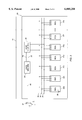
- FIG. 3 a multiple-register-access-capable device 20 according to the present invention is shown in block-diagram form.
- the multiple-register-access-capable device 20 of FIG. 3 communicates with the serial data link 14 and with other devices as shown in the architecture of FIG. 1
- the multiple-register-access-capable device 20 contains a plurality of registers 22a, 22b, 22c, 22d, 22e, 22f, and 22n. While the FIG. 3 depicts seven registers, those of ordinary skill in the art will recognize that this number is a matter of design choice as indicated by the breaks in the structure to the right of register 22f. For example, if the aforementioned IEEE protocol is used, there are a maximum of thirty-two registers, requiring a five-bit address field.
- a state machine 24 controls the flow of data between the serial link 14 and the multiple-register-access-capable device 20.
- state machine 20 may be readily implemented in hardware or software. Individual designs will depend on the particular serial link protocol used and will be simple design exercises given a defined protocol to implement.
- state machine is meant to include all hardware and software schemes known to those of ordinary skill in the art for controlling data flow in read and write operations between registers and a serial port.
- Port interface 26 is the bridge between serial link 14 and the registers 22a, 22b, 22c, 22d, 22e, 22f, and 22n and will contain the necessary conventional bus switching and driving circuitry to interface between the serial link 14 and the register address, data, and control busses 32, 34, and 36, respectively.
- the multiple-register-access-capable device 20 is configured to accept information indicating a multiple-register-access mode. When in this mode, device 20 interprets a read or write request identifying a preselected one of the registers 22a, 22b, 22c, 22d, 22e, 22f, and 22n as a read or write request for a preselected group of the registers 22a, 22b, 22c, 22d, 22e, 22f, and 22n.
- a Controller addresses this register by asserting a frame identifying this register in a selected multiple-register-access-capable device 20 configured according to the present invention
- the Controller is given access to a set of registers which may include all or less than all of the registers if the multiple-register-access-capable mode of the present invention has been enabled.
- Enablement of the multiple-register-access-capable mode of the present invention can be accomplished in numerous ways, for example, by setting one of the bits in a register to a defined logic state, a pin on the integrated circuit, a mechanical switch, etc.
- the state machine 24 interrogates the designated bit position and controls operation of the device 20 in accordance with the contents of the designated bit position in the register.
- register bit 38 in register 22a is set, a "one" in the designated bit position could be defined to enable the multiple-register-access-capable mode of the present invention and a "zero" in the designated bit position would define a single register access mode.
- a line 40 from state machine 24 is connected to I/O pad 42 of the integrated circuit containing device 20.
- I/O pad 42 may be grounded or connected to the positive supply rail either by hardwiring or by a switch (shown at reference numeral 44).
- Other methods of enablement are possible either through software or hardware and will readily suggest themselves to persons of ordinary skill in the art.
- register address thirty one is designated as the multiple register access mode register, although those of ordinary skill in the art will recognize that one of the other registers could be so designated.
- the Controller addresses register thirty one the device 20 provides access to a set of registers selected by the state machine 26. This set may include all of the registers including register address thirty one, it may include all registers except register thirty-one, or it may include some other preselected number of registers.
- FIG. 4 is a bit map of typical read and write packets addressed to a device such as the one in FIG. 3 and shows how the packet frame structure of the IEEE protocol shown in FIG. 2 could be modified to accommodate the multiple-register-access mode of the present invention, assuming that all thirty-two registers are accessed in a multiple register access cycle.
- the DATA field is expanded to 512 bits D0 through D511.
- the remaining sixteen bits contained in the other MI frame fields stay the same.
- the presently preferred order of the bits in the multiple register access DATA field consists of the bits from each register taken in sequential order from register address zero to register address thirty one.
- a comparison between the prior art and the presently disclosed invention demonstrates the advantage of the multiple register access apparatus and methods disclosed herein.
- the time required to access any one register, other than the multiple register access mode register is still sixty four clock cycles in the Physical Device.
- the time required to access all thirty two of the registers of the Physical Device is improved through the use of the multiple register access MI frame.
- the time required to access all thirty two of the registers of the Physical Device is improved from 2048 clock cycles in the prior art to only 560 clock cycles in the present invention.
- the total of 560 cycles is the sum of the thirty two cycles to establish the idle state of the Physical Device and the Controller and the 528 cycles of the multiple register access MI frame.
- FIG. 5 is a block diagram of such a system including a plurality of register-based serial port devices in accordance with the present invention connected to a serial port. As may be seen from FIG. 5, a serial link 14 may be driven by Controller 12. A plurality of multiple-register-access-capable devices 20a through 20c are shown connected to the serial link 14, as well as a plurality of prior art Physical Devices 16a and 16b.
- FIG. 5 illustrates that it is possible to configure a system in which some multiple-register-access-capable devices may be employed along with other register-based Physical Devices which do not have the features of the present invention.
- addressing the devices 16a and 16b and 20a through 20c is the same except that devices 16a and 16b and devices 20a through 20c will respond differently to multiple-register-access mode commands addressed to the designated register.
- Devices 16a and 16b will merely operate on the register actually addressed, whereas devices 20a through 20c will respond according to the teachings of the present invention.
- step 50 the state machine determines if it is in multiple-register access mode by examining the multiple-register-access enable indicator which, as previously mentioned, may take one of a number of forms. The process flow will take two different paths, depending on whether multiple-register access mode is enabled.
- decision diamond 52 determines whether it is a read frame or a write frame. If it is a read frame, at step 56 the data are read from the selected register, placed in a frame and sent out over the serial link. If it is a write frame, the incoming data are written to the selected register in step 58. Such read and write operations are well known in the art and will not be set forth in detail herein. After the read or write operation is finished, the process ends at step 60.
- step 62 If multiple-register-access mode has been enabled, the process proceeds to decision diamond 62, where it awaits the start of an information frame. This process step may be the same as step 52.
- step 64 examines the frame OP code and determines if it is a read frame or a write frame. Step 64 may be the same as step 54. If the frame is a read frame, step 66 reads the data from the first register in the group of registers designated in the multiple register access mode, placed in a frame and sent out over the serial port. Step 68 determines if the register just read was the last one in the group. If it was, the process ends at step 60. If it was not, step 70 reads the data from the next register in the group of registers designated in the multiple register access mode, placed in a frame and sent out over the serial port. Step 68 then again determines if the register just read was the last one in the group. Steps 68 and 70 are repeated until all registers in the group have been read.
- step 72 writes the first data byte to the first register in the group of registers designated in the multiple register access mode.
- Step 74 determines if the register just written to was the last one in the group. If it was, the process ends at step 60. If it was not, step 76 writes the next data byte to the next register in the group of registers designated in the multiple register access mode. Step 74 again determines if the register just written to was the last one in the group. Steps 76 and 74 are repeated until data have been written to all registers in the group.
Landscapes
- Engineering & Computer Science (AREA)
- Theoretical Computer Science (AREA)
- Computer Hardware Design (AREA)
- Microelectronics & Electronic Packaging (AREA)
- Physics & Mathematics (AREA)
- General Engineering & Computer Science (AREA)
- General Physics & Mathematics (AREA)
- Computer Security & Cryptography (AREA)
- Computer Networks & Wireless Communication (AREA)
- Signal Processing (AREA)
- Information Transfer Systems (AREA)
Abstract
Description
Claims (6)
Priority Applications (1)
| Application Number | Priority Date | Filing Date | Title |
|---|---|---|---|
| US09/100,270 US6085258A (en) | 1996-08-12 | 1998-06-19 | State machine for selectively performing an operation on a single or a plurality of registers depending upon the register address specified in a packet |
Applications Claiming Priority (2)
| Application Number | Priority Date | Filing Date | Title |
|---|---|---|---|
| US08/695,793 US5790888A (en) | 1996-08-12 | 1996-08-12 | State machine for selectively performing an operation on a single or a plurality of registers depending upon the register address specified in a packet |
| US09/100,270 US6085258A (en) | 1996-08-12 | 1998-06-19 | State machine for selectively performing an operation on a single or a plurality of registers depending upon the register address specified in a packet |
Related Parent Applications (1)
| Application Number | Title | Priority Date | Filing Date |
|---|---|---|---|
| US08/695,793 Continuation US5790888A (en) | 1996-08-12 | 1996-08-12 | State machine for selectively performing an operation on a single or a plurality of registers depending upon the register address specified in a packet |
Publications (1)
| Publication Number | Publication Date |
|---|---|
| US6085258A true US6085258A (en) | 2000-07-04 |
Family
ID=24794486
Family Applications (3)
| Application Number | Title | Priority Date | Filing Date |
|---|---|---|---|
| US08/695,793 Expired - Lifetime US5790888A (en) | 1996-08-12 | 1996-08-12 | State machine for selectively performing an operation on a single or a plurality of registers depending upon the register address specified in a packet |
| US09/100,270 Expired - Lifetime US6085258A (en) | 1996-08-12 | 1998-06-19 | State machine for selectively performing an operation on a single or a plurality of registers depending upon the register address specified in a packet |
| US09/118,337 Expired - Lifetime US6205493B1 (en) | 1996-08-12 | 1998-07-16 | State machine for selectively performing an operation on a single or a plurality of registers depending upon the register address specified in a packet |
Family Applications Before (1)
| Application Number | Title | Priority Date | Filing Date |
|---|---|---|---|
| US08/695,793 Expired - Lifetime US5790888A (en) | 1996-08-12 | 1996-08-12 | State machine for selectively performing an operation on a single or a plurality of registers depending upon the register address specified in a packet |
Family Applications After (1)
| Application Number | Title | Priority Date | Filing Date |
|---|---|---|---|
| US09/118,337 Expired - Lifetime US6205493B1 (en) | 1996-08-12 | 1998-07-16 | State machine for selectively performing an operation on a single or a plurality of registers depending upon the register address specified in a packet |
Country Status (1)
| Country | Link |
|---|---|
| US (3) | US5790888A (en) |
Cited By (9)
| Publication number | Priority date | Publication date | Assignee | Title |
|---|---|---|---|---|
| US20030097394A1 (en) * | 2001-09-25 | 2003-05-22 | Gerard Chauvel | Data transfer controlled by task attributes |
| US20050128962A1 (en) * | 2003-12-15 | 2005-06-16 | Finisar Corporation | Two-wire interface in which a master component monitors the data line during the preamble generation phase for synchronization with one or more slave components |
| US20060038587A1 (en) * | 2004-01-07 | 2006-02-23 | International Business Machines Corporation | Avoiding oscillation in self-synchronous bi-directional communication system |
| US8225024B2 (en) | 2004-03-05 | 2012-07-17 | Finisar Corporation | Use of a first two-wire interface communication to support the construction of a second two-wire interface communication |
| WO2016186840A1 (en) * | 2015-05-20 | 2016-11-24 | Honeywell International Inc. | Apparatus and method for multi-master solution on mdio communication bus |
| US9772665B2 (en) | 2012-10-05 | 2017-09-26 | Analog Devices, Inc. | Power switching in a two-wire conductor system |
| US9875152B2 (en) | 2011-10-05 | 2018-01-23 | Analog Devices, Inc. | Methods for discovery, configuration, and coordinating data communications between master and slave devices in a communication system |
| US9946679B2 (en) | 2011-10-05 | 2018-04-17 | Analog Devices, Inc. | Distributed audio coordination over a two-wire communication bus |
| US20220156219A1 (en) * | 2011-10-05 | 2022-05-19 | Analog Devices, Inc. | Two-wire communication systems and applications |
Families Citing this family (11)
| Publication number | Priority date | Publication date | Assignee | Title |
|---|---|---|---|---|
| US5978853A (en) * | 1996-09-16 | 1999-11-02 | Advanced Micro Devices, Inc. | Address administration for 100BASE-T PHY devices |
| US6073128A (en) * | 1997-10-31 | 2000-06-06 | Oracle Corporation | Method and apparatus for identifying files used to restore a file |
| US5948076A (en) * | 1997-12-31 | 1999-09-07 | Adaptec, Inc. | Method and system for changing peripheral component interconnect configuration registers |
| US6256732B1 (en) * | 1998-06-25 | 2001-07-03 | International Business Machines Corporation | Computer system having automatic registration for in-box configuration |
| US6970983B1 (en) * | 2002-10-28 | 2005-11-29 | Lsi Logic Corporation | Multiple port system and method for controlling the same |
| US7509439B2 (en) * | 2005-01-27 | 2009-03-24 | Standard Microsystems Corporation | Method for maintaining register integrity and receive packet protection during ULPI PHY to LINK bus transactions |
| US7587539B2 (en) * | 2006-04-25 | 2009-09-08 | Texas Instruments Incorporated | Methods of inter-integrated circuit addressing and devices for performing the same |
| TWI355822B (en) * | 2007-12-20 | 2012-01-01 | Realtek Semiconductor Corp | Circuit and method for setting data and their appl |
| US9063831B1 (en) * | 2012-12-21 | 2015-06-23 | Cadence Design Systems, Inc. | Method and apparatus for optimizing access to control registers in an emulation chip |
| GB2549722B (en) * | 2016-04-25 | 2018-09-26 | Imagination Tech Ltd | Communications interface circuit architecture |
| US10068648B1 (en) * | 2017-08-30 | 2018-09-04 | Micron Technology, Inc. | Distributed mode registers in memory devices |
Citations (2)
| Publication number | Priority date | Publication date | Assignee | Title |
|---|---|---|---|---|
| US5966731A (en) * | 1995-10-19 | 1999-10-12 | Rambus, Inc. | Protocol for communication with dynamic memory |
| US6021477A (en) * | 1989-05-05 | 2000-02-01 | Samsung Electronics Co., Ltd | Multiple mode memory module |
Family Cites Families (16)
| Publication number | Priority date | Publication date | Assignee | Title |
|---|---|---|---|---|
| US4435792A (en) * | 1982-06-30 | 1984-03-06 | Sun Microsystems, Inc. | Raster memory manipulation apparatus |
| DE3684270D1 (en) * | 1985-12-27 | 1992-04-16 | Toshiba Kawasaki Kk | METHOD AND COMMUNICATION NETWORK FOR LIMITED BROADCASTING. |
| JPS62278651A (en) * | 1986-05-28 | 1987-12-03 | Hitachi Ltd | Partial writing controller |
| US5056015A (en) * | 1988-03-23 | 1991-10-08 | Du Pont Pixel Systems Limited | Architectures for serial or parallel loading of writable control store |
| US4896265A (en) * | 1988-03-28 | 1990-01-23 | General Electric Company | Parallel broadcasting method and apparatus |
| US5113507A (en) * | 1988-10-20 | 1992-05-12 | Universities Space Research Association | Method and apparatus for a sparse distributed memory system |
| FR2638923B1 (en) | 1988-11-08 | 1990-12-21 | Bull Sa | LOCAL NETWORK TRANSMISSION MEDIA ACCESS UNIT |
| US4984251A (en) | 1989-08-16 | 1991-01-08 | National Semiconductor Corporation | Method and apparatus for the synchronization of a cascaded multi-channel data transmission |
| JP2526691B2 (en) * | 1990-03-02 | 1996-08-21 | 三菱電機株式会社 | Programmable controller control method |
| JP3394542B2 (en) * | 1990-03-30 | 2003-04-07 | テキサス インスツルメンツ インコーポレイテツド | Serial data input / output test equipment |
| US5249183A (en) | 1991-03-14 | 1993-09-28 | Level One Communications, Inc. | Interfacing unit for local area networks |
| US5179554A (en) | 1991-04-08 | 1993-01-12 | Digital Equipment Corporation | Automatic association of local area network station addresses with a repeater port |
| US5287503A (en) * | 1991-09-27 | 1994-02-15 | Sun Microsystems, Inc. | System having control registers coupled to a bus whereby addresses on the bus select a control register and a function to be performed on the control register |
| US5251203A (en) | 1991-12-23 | 1993-10-05 | Xerox Corporation | Hub privacy filter for active star CSMA/CD network |
| US5542067A (en) * | 1992-04-23 | 1996-07-30 | International Business Machines Corporation | Virtual multi-port RAM employing multiple accesses during single machine cycle |
| CA2141268C (en) * | 1994-01-28 | 1999-09-21 | Masanobu Inaba | High-speed synchronization communication control mechanism for multi-processor system |
-
1996
- 1996-08-12 US US08/695,793 patent/US5790888A/en not_active Expired - Lifetime
-
1998
- 1998-06-19 US US09/100,270 patent/US6085258A/en not_active Expired - Lifetime
- 1998-07-16 US US09/118,337 patent/US6205493B1/en not_active Expired - Lifetime
Patent Citations (2)
| Publication number | Priority date | Publication date | Assignee | Title |
|---|---|---|---|---|
| US6021477A (en) * | 1989-05-05 | 2000-02-01 | Samsung Electronics Co., Ltd | Multiple mode memory module |
| US5966731A (en) * | 1995-10-19 | 1999-10-12 | Rambus, Inc. | Protocol for communication with dynamic memory |
Cited By (16)
| Publication number | Priority date | Publication date | Assignee | Title |
|---|---|---|---|---|
| US20030097394A1 (en) * | 2001-09-25 | 2003-05-22 | Gerard Chauvel | Data transfer controlled by task attributes |
| US7712098B2 (en) * | 2001-09-25 | 2010-05-04 | Texas Instruments Incorporated | Data transfer controlled by task attributes |
| US20050128962A1 (en) * | 2003-12-15 | 2005-06-16 | Finisar Corporation | Two-wire interface in which a master component monitors the data line during the preamble generation phase for synchronization with one or more slave components |
| US8667194B2 (en) * | 2003-12-15 | 2014-03-04 | Finisar Corporation | Two-wire interface in which a master component monitors the data line during the preamble generation phase for synchronization with one or more slave components |
| US20060038587A1 (en) * | 2004-01-07 | 2006-02-23 | International Business Machines Corporation | Avoiding oscillation in self-synchronous bi-directional communication system |
| US7353308B2 (en) * | 2004-01-07 | 2008-04-01 | International Business Machines Corporation | Avoiding oscillation in self-synchronous bi-directional communication system |
| US8225024B2 (en) | 2004-03-05 | 2012-07-17 | Finisar Corporation | Use of a first two-wire interface communication to support the construction of a second two-wire interface communication |
| US10311010B2 (en) | 2011-10-05 | 2019-06-04 | Analog Devices, Inc. | Two-wire communication systems and applications |
| US9875152B2 (en) | 2011-10-05 | 2018-01-23 | Analog Devices, Inc. | Methods for discovery, configuration, and coordinating data communications between master and slave devices in a communication system |
| US9946679B2 (en) | 2011-10-05 | 2018-04-17 | Analog Devices, Inc. | Distributed audio coordination over a two-wire communication bus |
| US20220156219A1 (en) * | 2011-10-05 | 2022-05-19 | Analog Devices, Inc. | Two-wire communication systems and applications |
| US11874791B2 (en) * | 2011-10-05 | 2024-01-16 | Analog Devices, Inc. | Two-wire communication systems and applications |
| US9772665B2 (en) | 2012-10-05 | 2017-09-26 | Analog Devices, Inc. | Power switching in a two-wire conductor system |
| US9946680B2 (en) | 2012-10-05 | 2018-04-17 | Analog Devices, Inc. | Peripheral device diagnostics and control over a two-wire communication bus |
| WO2016186840A1 (en) * | 2015-05-20 | 2016-11-24 | Honeywell International Inc. | Apparatus and method for multi-master solution on mdio communication bus |
| US10572436B2 (en) | 2015-05-20 | 2020-02-25 | Honeywell International Inc. | Apparatus and method for multi-master solution on MDIO communication bus |
Also Published As
| Publication number | Publication date |
|---|---|
| US5790888A (en) | 1998-08-04 |
| US6205493B1 (en) | 2001-03-20 |
Similar Documents
| Publication | Publication Date | Title |
|---|---|---|
| US6085258A (en) | State machine for selectively performing an operation on a single or a plurality of registers depending upon the register address specified in a packet | |
| EP2350847B1 (en) | Method and system for improving serial port memory communication latency and reliability | |
| US6185630B1 (en) | Device initializing system with programmable array logic configured to cause non-volatile memory to output address and data information to the device in a prescribed sequence | |
| US5892922A (en) | Virtual local area network memory access system | |
| JP2584957B2 (en) | Host-directed device | |
| JPH03154452A (en) | Switch for making dynamic connection and protocol | |
| CN1965285A (en) | Apparatus and method for direct memory access in a hub-based memory system | |
| US10996950B2 (en) | Apparatuses and methods involving selective disablement of side effects caused by accessing register sets | |
| US5574869A (en) | Bus bridge circuit having configuration space enable register for controlling transition between various modes by writing the bridge identifier into CSE register | |
| US5729755A (en) | Process for transmitting data in a data processing system with distributed computer nodes, communicating via a serial data bus, between which data messages are exchanged, tested for acceptance in a computer node, and stored temporarily | |
| JPS6194437A (en) | Multistage packet exchange network | |
| JPH04279954A (en) | Data transfer system for device controller | |
| EP0506481B1 (en) | Communication apparatus | |
| US6266336B1 (en) | Apparatus and method for setting A/C bits in token ring frames for switches | |
| EP0419750B1 (en) | Distribution mechanism for establishing communications between user interfaces of a communication system | |
| EP0309676B1 (en) | Workstation controller with full screen write mode and partial screen write mode | |
| US20050273546A1 (en) | Analog signal processor, as well as, a data register rewriting method and a data transmission method thereof | |
| WO1998041924A1 (en) | Methods and apparatus for arbitrating and controlling arbitration for access to a serial bus | |
| EP0261947A1 (en) | Computer system | |
| EP0382342B1 (en) | Computer system DMA transfer | |
| EP0569512A4 (en) | Packet transmission system and method utilizing both a data bus and dedicated control lines | |
| JP3436984B2 (en) | Traffic shaping device for ATM communication system | |
| EP0076494A2 (en) | Data transmission bus system for a plurality of processors | |
| US6970983B1 (en) | Multiple port system and method for controlling the same | |
| SU1151976A1 (en) | Data exchange control unit |
Legal Events
| Date | Code | Title | Description |
|---|---|---|---|
| STCF | Information on status: patent grant |
Free format text: PATENTED CASE |
|
| FEPP | Fee payment procedure |
Free format text: PAT HOLDER NO LONGER CLAIMS SMALL ENTITY STATUS, ENTITY STATUS SET TO UNDISCOUNTED (ORIGINAL EVENT CODE: STOL); ENTITY STATUS OF PATENT OWNER: LARGE ENTITY |
|
| FPAY | Fee payment |
Year of fee payment: 4 |
|
| FEPP | Fee payment procedure |
Free format text: PAYER NUMBER DE-ASSIGNED (ORIGINAL EVENT CODE: RMPN); ENTITY STATUS OF PATENT OWNER: LARGE ENTITY Free format text: PAYOR NUMBER ASSIGNED (ORIGINAL EVENT CODE: ASPN); ENTITY STATUS OF PATENT OWNER: LARGE ENTITY |
|
| FPAY | Fee payment |
Year of fee payment: 8 |
|
| AS | Assignment |
Owner name: LSI LOGIC CORPORATION, CALIFORNIA Free format text: MERGER;ASSIGNOR:SEEQ TECHNOLOGY INCORPORATED;REEL/FRAME:020431/0158 Effective date: 19990825 Owner name: LSI CORPORATION, CALIFORNIA Free format text: MERGER;ASSIGNOR:LSI LOGIC CORPORATION;REEL/FRAME:020431/0176 Effective date: 20070404 Owner name: SEEQ TECHNOLOGY INCORPORATED, CALIFORNIA Free format text: MERGER;ASSIGNOR:STEALTH ACQUISITION CORPORATION;REEL/FRAME:020431/0065 Effective date: 19990622 |
|
| FPAY | Fee payment |
Year of fee payment: 12 |
|
| AS | Assignment |
Owner name: DEUTSCHE BANK AG NEW YORK BRANCH, AS COLLATERAL AG Free format text: PATENT SECURITY AGREEMENT;ASSIGNORS:LSI CORPORATION;AGERE SYSTEMS LLC;REEL/FRAME:032856/0031 Effective date: 20140506 |
|
| AS | Assignment |
Owner name: AVAGO TECHNOLOGIES GENERAL IP (SINGAPORE) PTE. LTD Free format text: ASSIGNMENT OF ASSIGNORS INTEREST;ASSIGNOR:LSI CORPORATION;REEL/FRAME:035390/0388 Effective date: 20140814 |
|
| AS | Assignment |
Owner name: AGERE SYSTEMS LLC, PENNSYLVANIA Free format text: TERMINATION AND RELEASE OF SECURITY INTEREST IN PATENT RIGHTS (RELEASES RF 032856-0031);ASSIGNOR:DEUTSCHE BANK AG NEW YORK BRANCH, AS COLLATERAL AGENT;REEL/FRAME:037684/0039 Effective date: 20160201 Owner name: LSI CORPORATION, CALIFORNIA Free format text: TERMINATION AND RELEASE OF SECURITY INTEREST IN PATENT RIGHTS (RELEASES RF 032856-0031);ASSIGNOR:DEUTSCHE BANK AG NEW YORK BRANCH, AS COLLATERAL AGENT;REEL/FRAME:037684/0039 Effective date: 20160201 |
|
| AS | Assignment |
Owner name: BANK OF AMERICA, N.A., AS COLLATERAL AGENT, NORTH CAROLINA Free format text: PATENT SECURITY AGREEMENT;ASSIGNOR:AVAGO TECHNOLOGIES GENERAL IP (SINGAPORE) PTE. LTD.;REEL/FRAME:037808/0001 Effective date: 20160201 Owner name: BANK OF AMERICA, N.A., AS COLLATERAL AGENT, NORTH Free format text: PATENT SECURITY AGREEMENT;ASSIGNOR:AVAGO TECHNOLOGIES GENERAL IP (SINGAPORE) PTE. LTD.;REEL/FRAME:037808/0001 Effective date: 20160201 |
|
| AS | Assignment |
Owner name: AVAGO TECHNOLOGIES GENERAL IP (SINGAPORE) PTE. LTD., SINGAPORE Free format text: TERMINATION AND RELEASE OF SECURITY INTEREST IN PATENTS;ASSIGNOR:BANK OF AMERICA, N.A., AS COLLATERAL AGENT;REEL/FRAME:041710/0001 Effective date: 20170119 Owner name: AVAGO TECHNOLOGIES GENERAL IP (SINGAPORE) PTE. LTD Free format text: TERMINATION AND RELEASE OF SECURITY INTEREST IN PATENTS;ASSIGNOR:BANK OF AMERICA, N.A., AS COLLATERAL AGENT;REEL/FRAME:041710/0001 Effective date: 20170119 |