US6033988A - Film forming methods - Google Patents
Film forming methods Download PDFInfo
- Publication number
- US6033988A US6033988A US09/014,091 US1409198A US6033988A US 6033988 A US6033988 A US 6033988A US 1409198 A US1409198 A US 1409198A US 6033988 A US6033988 A US 6033988A
- Authority
- US
- United States
- Prior art keywords
- solvent
- coating film
- film
- dropwise dispensing
- semiconductor wafer
- Prior art date
- Legal status (The legal status is an assumption and is not a legal conclusion. Google has not performed a legal analysis and makes no representation as to the accuracy of the status listed.)
- Expired - Fee Related
Links
Images


Classifications
-
- H—ELECTRICITY
- H10—SEMICONDUCTOR DEVICES; ELECTRIC SOLID-STATE DEVICES NOT OTHERWISE PROVIDED FOR
- H10P—GENERIC PROCESSES OR APPARATUS FOR THE MANUFACTURE OR TREATMENT OF DEVICES COVERED BY CLASS H10
- H10P72/00—Handling or holding of wafers, substrates or devices during manufacture or treatment thereof
- H10P72/04—Apparatus for manufacture or treatment
- H10P72/0448—Apparatus for applying a liquid, a resin, an ink or the like
-
- B—PERFORMING OPERATIONS; TRANSPORTING
- B05—SPRAYING OR ATOMISING IN GENERAL; APPLYING FLUENT MATERIALS TO SURFACES, IN GENERAL
- B05C—APPARATUS FOR APPLYING FLUENT MATERIALS TO SURFACES, IN GENERAL
- B05C11/00—Component parts, details or accessories not specifically provided for in groups B05C1/00 - B05C9/00
- B05C11/02—Apparatus for spreading or distributing liquids or other fluent materials already applied to a surface ; Controlling means therefor; Control of the thickness of a coating by spreading or distributing liquids or other fluent materials already applied to the coated surface
- B05C11/08—Spreading liquid or other fluent material by manipulating the work, e.g. tilting
-
- B—PERFORMING OPERATIONS; TRANSPORTING
- B05—SPRAYING OR ATOMISING IN GENERAL; APPLYING FLUENT MATERIALS TO SURFACES, IN GENERAL
- B05D—PROCESSES FOR APPLYING FLUENT MATERIALS TO SURFACES, IN GENERAL
- B05D1/00—Processes for applying liquids or other fluent materials
- B05D1/002—Processes for applying liquids or other fluent materials the substrate being rotated
- B05D1/005—Spin coating
Definitions
- the present invention relates to film forming methods for forming coating films through spin coating of solution on substrates, and particularly relates to film forming methods adapted for forming photoresist films, SOG (Spin On Glass) films, etc. on semiconductor substrates (semiconductor wafers).
- SOG Spin On Glass
- a spin coating method as a method for forming films, such as photoresist films, SOG (Spin On Glass) films, etc., on semiconductor wafers.
- a semiconductor wafer is horizontally held and spun, while droplets of solution are dropped on the semiconductor wafer before and after the start of the spin of the semiconductor wafer, whereby a film of the solution is formed on the semiconductor wafer by centrifugal force caused by the spin of the semiconductor wafer.
- films are formed also at peripheral portions of the semiconductor wafer.
- the semiconductor wafer, at the peripheral portions of which coating films are formed is accommodated into, for example, a cassette, a contact of the films formed at the peripheral portions of the semiconductor wafer with the cassette causes dust from the films. Introducing of the dust into a semiconductor device causes a malfunction of the semiconductor device.
- a solvent is dropped at the peripheral portions of the semiconductor wafer so as to remove the films formed at the peripheral portions of the semiconductor wafer.
- FIGS. 5-7 are cross-sectional views each showing a process for forming the SOG film on the semiconductor wafer.
- a droplet of solution 53 in which a material of the SOG film is dissolved, is dropped onto a surface 51a of a semiconductor wafer 51 having a disk configuration, the wafer 51 being fixed on a spin chuck 52 for spinning the semiconductor wafer 51. And thereafter, the semiconductor wafer 51 is spun, for example, at 3000 rpm. When the semiconductor wafer 51 is spun, centrifugal force of the spin causes a coating film 54 by solution 53 to form over a surface 51a to edges 51b of the semiconductor wafer 51 as shown in FIG. 6.
- a solvent 56 is dropped at a position near inside the periphery of the semiconductor wafer 51, while the semiconductor wafer 51 is kept on spinning.
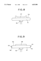
- FIGS. 8 and 9 are illustrations each showing the state in which films formed on the peripheral portions of the semiconductor wafer 51 have been removed by means of dropping solvents as shown in FIG. 7.
- Japanese Patent Application Laid Open Gazette Hei. 9-220505 discloses a method in which in FIG. 7, as the solvent 56 to be dropped, solvents having a weak affinity for the coating film 54 covering the surface 51a of the semiconductor wafer 51, are used.
- solvents having a weak affinity for the coating film 54 covering the surface 51a of the semiconductor wafer 51 are dropped, as shown in FIG. 9, as to a film 58 of the solution retaining on the surface 51a of the semiconductor wafer 51, an occurrence of protuberances of the peripheral portions of the film 58 are avoided, but a film 59 will be retained at the edges 51b of the semiconductor wafer 51.
- Accommodating such a semiconductor wafer having the films at its edges into a cassette involves such a problem that dust is generated owing to a contact of the films remaining at the edges of the semiconductor wafer with the cassette at the time of the accommodation of the semiconductor wafer.
- any of these schemes involves such problems that protuberances of edge portions of the film 57 retained on the surface 51a of the semiconductor wafer 51 occur, or the film 59 is retained at the edges 51b of the semiconductor wafer 51, and thus finally it is impossible to avoid the problem of a generation of dust.
- A, B, C, D and E are Type 7 produced by TOKYO OHKA KOGYOU Co., LTD.
- Type 2 produced by TOKYO OHKA KOGYOU Co., LTD.
- FOX-15 produced by Toray Dow Corning Co., LTD.
- Type 10 produced by TOKYO OHKA KOGYOU Co., LTD.
- Type 12 produced by TOKYO OHKA KOGYOU Co., LTD., respectively.
- the 4 types of solvents a, b, c and d are isopropyl alcohol, cyclohexanone, ⁇ -butyrolactone, MIBK, respectively.
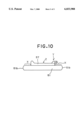
- FIG. 10 is an explanatory view useful for understanding an evaluation method of three evaluation items (an appearance, a protuberance and an edge bead residual) shown in Table 1.
- the "Appearance” shown in Table 1 indicates whether film residuals occur on regions X (shown in FIG. 10) of the semiconductor wafer 51. In case of no film residual, the “Appearance” is denoted by “Good”. In the event that film residuals exist, the “Appearance” is denoted by "Residuals Exist”.
- the "protuberance” indicates a difference H between the thickness of the peripheral portions Y and the thickness of the central portion Z of the film 57 remaining on the surface 51a of the semiconductor wafer 51 when the solvent 56 is dropped on the semiconductor wafer 51.
- the “Edge bead residual” indicates whether edge bead residuals occur on the edges 51b of the semiconductor wafer 51. In case of no edge bead residual, the “Edge bead residual” is denoted by “Non”. In the event that edge bead residuals exist, the “Edge bead residual" is denoted by the "Present”.
- Japanese Patent Application Laid Open Gazette Hei. 6-168872 discloses a method in which prior to dropping the SOG solvent onto a semiconductor wafer, the peripheral portions of the semiconductor wafer are treated with HMDS (hexamethyldisilazane) or the like so that the water-repellency can be brought about. According to this method, after the peripheral portions of the semiconductor wafer are subjected to a water-repellent treatment, solution is dropped, and the semiconductor wafer is spun.
- HMDS hexamethyldisilazane
- the solution which is spread as a film toward the peripheral portions of the semiconductor wafer by centrifugal force, is shed on the peripheral portions exhibiting the water-repellency, so that the film is formed only at the central area of the semiconductor wafer.
- the water-repellency is brought about on only the peripheral portions of the semiconductor wafer.
- the semiconductor wafer is subjected to the HMDS atmosphere in its entirety.
- a film (hereinafter, referred to as a CVD film) produced by, for example, the chemical vapor deposition, is formed on a semiconductor wafer, and after the peripheral portions of the semiconductor wafer on which the CVD film has been formed is treated so that the water-repellency is brought about, solution is dropped to form a coating film.
- a coating film with the CVD film is extremely degraded.
- a semiconductor device is manufactured in the condition that the adhesion of the films is degraded as mentioned above, then it may happen that a malfunction of the semiconductor device is brought about.
- Japanese Patent Application Laid Open Gazette Hei. 8-17817 discloses a method in which after the SOG solution is dropped onto a semiconductor wafer to form a coating film, hydrofluoric acid is dropped at the periphery of the SOG coating film so as to remove the peripheral portions of the coating film.
- hydrofluoric acid is used in view of the matter that going of hydrofluoric acid into another film not necessary to be removed causes deterioration of a semiconductor device, and also in view of the fact that hydrofluoric acid is poisonous.
- a film forming method having a spin coating process of forming a coating film through spin coating of a solution on a substrate, said film forming method comprising steps of:
- step (b) initiating dropping of a second solvent having a relatively high affinity for the coating film at a position closer to the periphery of the substrate as compared with the position of dropping of the first solvent, in a simultaneous timing as an initiation of dropping of the first solvent, or a timing later than the initiation of dropping of the first solvent. And it is preferable to follow step (c) and (d), which is described underneath, after said step (b).
- the film forming method of the present invention after a coating film is formed through spin coating of a solution on a substrate in order to remove the coating film, which are formed on the periphery of the substrate, and in addition, in order to retain a film involving no protuberance on the edge portions of the coating film, there are used both the first solvent having a relatively low affinity for the coating film and the second solvent having a relatively high affinity for the coating film.
- a dropping position of the second solvent is a position closer to the periphery of the substrate as compared with a position of dropping of the first solvent.
- the position of dropping of the first solvent is closer to the center of the substrate as the dropping position of the second solvent.
- a timing of the dropping of the second solvent it is a simultaneous timing as an initiation of dropping of the first solvent, or a timing later than the initiation of dropping of the first solvent. This feature makes it possible to prevent the second solvent, having a relatively high affinity for the coating film on the substrate, from flowing toward the center of the substrate.
- the use of the solvent having a relatively low affinity for the coating film on the substrate, as the first solvent makes it possible to form on the surface of the substrate a planar film involving no protuberance on the periphery by dropping of the first solvent and the second solvent.
- the second solvent having a relatively high affinity for the coating film is dropped at the position closer to the periphery of the substrate as compared with a position of dropping of the first solvent. This feature makes it possible to remove the coating film formed on the periphery of the substrate. That is, it is possible to form a planar film on the substrate, and also to prevent the residual of films on the edges of the substrate.
- said spin coating process forms an SOG film on a semiconductor substrate.
- said first solvent is cyclohexanone
- said second solvent is isopropyl alcohol.
- the film forming method according to the present invention is applied for forming the SOG film on the semiconductor substrate, it is effective that the steps (a) to (d) are executed while said semiconductor substrate is spun at a rotational speed between 2000 rpm and 3000 rpm.
- This feature makes it possible to effectively use the dropped first and second solvents so as to eliminate the edge beads of the SOG film formed on the semiconductor substrate.
- step (b) is to initiate dropping of the second solvent in a timing later than the initiation of dropping of the first solvent, and after the initiation of dropping of the first solvent in said step (a), the rotational speed of said semiconductor substrate is altered, and then said step (b) is executed.
- said spin coating process forms a photoresist film on a semiconductor substrate.
- said first solvent is cyclohexanone
- said second solvent is methyl-3-methoxypropionate.
- the steps (a) to (d) are executed while said semiconductor substrate is spun at a rotational speed between 2000 rpm and 3000 rpm. It is also preferable that the step (b) is to initiate dropping of the second solvent in a timing later than the initiation of dropping of the first solvent, and after the initiation of dropping of the first solvent in said step (a), the rotational speed of said semiconductor substrate is altered, and then said step (b) is executed. The reason why this is to do so is the same as the SOG film.
- the film forming method according to the present invention as such a typical concept that a solvent has a relatively low affinity for the coating film, or a solvent has a relatively high affinity for the coating film, there is adopted such a concept that the coating film is hard to dissolve (including insoluble) or easy to dissolve (or soluble).
- a film forming method having a spin coating process of forming a coating film through spin coating of a solution on a substrate, said film forming method comprising steps of:
- step (b) initiating dropping of a second solvent, into which the coating film is easy to dissolve, at a position closer to the periphery of the substrate as compared with the position of dropping of the first solvent, in a simultaneous timing as an initiation of dropping of the first solvent, or a timing later than the initiation of dropping of the first solvent. And it is preferable to follow step (c) and (d), which is described underneath, after said step (b).
- said spin coating process forms an SOG film on a semiconductor substrate.
- said first solvent is cyclohexanone
- said second solvent is isopropyl alcohol.
- the steps (a) to (d) are executed while said semiconductor substrate is spun at a rotational speed between 2000 rpm and 3000 rpm. It is also preferable that said step (b) is to initiate dropping of the second solvent in a timing later than the initiation of dropping of the first solvent, and after the initiation of dropping of the first solvent in said step (a), the rotational speed of said semiconductor substrate is altered, and then said step (b) is executed.
- a solute in the coating film is hard to dissolve (including insoluble) or easy to dissolve (or soluble) in a solvent.
- a film forming method having a spin coating process of forming a coating film through spin coating of a solution on a substrate, said film forming method comprising steps of:
- said spin coating process forms an SOG film on a semiconductor substrate.
- said first solvent is cyclohexanone
- said second solvent is isopropyl alcohol.
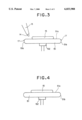
- FIG. 1 is a sectional view useful for understanding a manufacturing process in a film forming method according to an embodiment of the present invention
- FIG. 2 is a sectional view useful for understanding a manufacturing process in a film forming method according to an embodiment of the present invention
- FIG. 3 is a sectional view useful for understanding a manufacturing process in a film forming method according to an embodiment of the present invention
- FIG. 4 is a sectional view useful for understanding a manufacturing process in a film forming method according to an embodiment of the present invention
- FIG. 5 is a sectional view showing the state in which solution is dropped onto a semiconductor wafer
- FIG. 6 is a sectional view showing the state in which a coating film is formed on the semiconductor wafer
- FIG. 7 is a sectional view showing the state in which solvents are dropped onto the film formed on the semiconductor wafer
- FIG. 8 is a sectional view showing the state in which a film is formed on the semiconductor wafer after solvents are dropped;
- FIG. 9 is a sectional view showing the state in which a film is formed on the semiconductor wafer after solvents, which are different from that of FIG. 8, are dropped.
- FIG. 10 is an explanatory view useful for understanding an evaluation method of three evaluation items (an appearance, a protuberance and an edge bead residual) shown in Table 1.
- FIGS. 5 and 6 A film forming method according to an embodiment of the present invention will be explained, first, referring to FIGS. 5 and 6, and then referring to FIGS. 1 to 4.
- a droplet of solution 53 in which a material of the SOG film is dissolved, is dropped onto the surface 51a of the semiconductor wafer 51. Thereafter, the semiconductor wafer 51 is spun to form the coating film 54 (SOG film) as shown in FIG. 6, and the following processes are practiced.
- cyclohexanone 12 which is a solvent having a weak affinity for the SOG film
- dropping of cyclohexanone 12 is initiated through a nozzle 11 at the position inside 4 mm from the periphery of the semiconductor wafer 51.
- the semiconductor wafer 51 is either in a stationary state or a spinning state.
- the semiconductor wafer 51 is spun at 3000 rpm, and after 2 seconds since dropping of cyclohexanone 12 is initiated, as shown in FIG. 2, dropping of isopropyl alcohol 14, which is a solvent having a stronger affinity for the SOG film or the coating film 54 as compared with cyclohexanone 12, is initiated through a nozzle 13 at the position inside 2 mm from the periphery of the semiconductor wafer 51.
- Isopropyl alcohol 14 is a solvent into which the SOG film is soluble, and specifically a solvent in which silicon compounds and silicon polymers, which are solutes in the SOG film, are soluble.
- a planar coating film 15 exists on the surface 51a of the semiconductor wafer 51, and a coating film 16 is spread also on the edges 51b of the semiconductor wafer 51.
- the semiconductor wafer 51 is spun, so that the coating film 54 is formed. It is acceptable, however, that first the semiconductor wafer 51 is spun at low speed, and then the solution 53 is dropped onto the semiconductor wafer 51, so that the coating film 54 is formed on the semiconductor wafer 51.
- the semiconductor wafer is spun at 3000 rpm.
- any one is acceptable, as a rotational speed of the semiconductor wafer, which generates centrifugal force in such an extent that the coating films formed on the peripheral portions of the semiconductor wafer, are removed by solvents dropped onto the semiconductor wafer.
- cyclohexanone 12 and isopropyl alcohol 14 are simultaneously initiated in dropping of their droplets.
- cyclohexanone 12 is used as the solvent to be dropped at the position more apart from the periphery of the semiconductor wafer 51, or at the position closer to the center of the semiconductor wafer 51.
- any one other than cyclohexanone 12 is acceptable, as a solvent, which has a weak affinity for the coating film 54 in such an extent that no protuberance occurs on the peripheral portions of the coating film 15 to be retained on the semiconductor wafer 51.
- isopropyl alcohol 14 is used as the solvent to be dropped at the position closer to the periphery of the semiconductor wafer 51.
- the solvent e.g. cyclohexanone 12, in the present embodiment
- a droplet of solution 53 in which a material of photoresist is dissolved, is dropped onto the surface 51a of the semiconductor wafer 51. Thereafter, the semiconductor wafer 51 is spun to form the coating film 54 (photoresist film) as shown in FIG. 6.
- the semiconductor wafer 51 is spun at 2500 rpm, and the following processes are practiced.
- the photoresist material goods on the market, which consist of "novolac resin", are used.
- cyclohexanone 12 which is a first solvent offering no affinity for a solvent contained in the solution 53 dropped onto the surface 51a of the semiconductor wafer 51 (that is, the first solvent is remarkably different from the solution 53 in contact angle or surface tension)
- cyclohexanone 12 is a first solvent offering no affinity for a solvent contained in the solution 53 dropped onto the surface 51a of the semiconductor wafer 51 (that is, the first solvent is remarkably different from the solution 53 in contact angle or surface tension
- MMP thinner methyl-3-methoxypropionate 14
- MMP thinner 14 is a second solvent offering affinity for a solvent contained in the solution 53 dropped onto the surface 51a of the semiconductor wafer 51 (that is, the second solvent is small in contact angle or surface tension as compared with the solution 53)
- MMP thinner 14 is dropped, as shown in FIG. 2, the planar coating film 15 exists on the surface 51a of the semiconductor wafer 51, and the coating film 16 is spread also on the edges 51b of the semiconductor wafer 51.
- cyclohexanone is used as the solvent offering no affinity for a solvent contained in the solution 53 in which the photoresist material is dissolved. It is acceptable, however, that instead of cyclohexanone, for example, lactic acid and OK 73 thinner (mixed liquid of PGMEA and PGME) are used.
- MMP thinner is used as the solvent offering affinity for a solvent contained in the solution 53 in which the photoresist material is dissolved (that is, the solvent is small in contact angle or surface tension as compared with the solution 53.
- MMP thinner is used as a solvent, which offers affinity for a solvent contained in the solution 53 (that is, the solvent is small in contact angle or surface tension as compared with the solution 53).
- a CVD film is formed on a semiconductor wafer, and the peripheral portions of the semiconductor wafer are treated with HMDS (hexamethyldisilazane) or the like so that the water-repellency can be brought about. Thereafter, solution is dropped onto the semiconductor wafer so as to form the SOG film.
- HMDS hexamethyldisilazane
- solution is dropped onto the semiconductor wafer so as to form the SOG film.
- HMDS hexamethyldisilazane
- the film forming method according to the present invention there is no need to bring about the water-repellency using HMDS.
- the film forming method of the present invention even if a coating film is formed on the semiconductor wafer on which the CVD film has been formed, it is possible to avoid the degradation of the adhesion of the SOG film to the CVD film.
- the film forming method of the present invention it is possible to form a film on a semiconductor wafer without dropping hydrofluoric acid onto the semiconductor wafer. Further, it is possible to prevent the residual of films on the peripheral portions of the semiconductor wafer, and also to form a film on the semiconductor wafer involving no protuberance on the periphery.
Landscapes
- Materials For Photolithography (AREA)
- Application Of Or Painting With Fluid Materials (AREA)
Abstract
Description
                                  TABLE 1
__________________________________________________________________________
a (Isopropyl alcohol)
                 b (Cyclohexanone)
                               c (γ-butyrolactone
                                               d (MIBK)
Appear- Protu-
            Edge bead
                 Appear-
                     Protu-
                          Edge bead  Protu-
                                          Edge bead  Protu-
                                                          Edge bead
ance    berance
            residuals
                 ance
                     berance
                          residuals
                               Appearance
                                     berance
                                          residuals
                                               Appearance
                                                     berance
                                                          residuals
__________________________________________________________________________
A   Good
        Not less
            Non  Good
                     Non  present
                               Residuals
                                     Not less
                                          present
                                               Residuals
                                                     Not
                                                          present
(Type   than                   Exist 0.1 μm Exist than
7)      1.0 μm                                    0.5 μm
B   Good
        Not less
            Non  Good
                     Not less
                          present
                               Good  Non  present
                                               Residuals
                                                     Not
                                                          present
(Type   than         than                      Exist than
2)      1.0 μm    0.4 μm                       0.3 μm
C   Unavailable  Good
                     Non  present
                               Unavailable     Good  Not
                                                          present
(FOX)                                                than
                                                     1.0 μm
D   Good
        Not less
            Non  Good
                     Non  present
                               Residuals
                                     Not less
                                          present
                                               Residuals
                                                     Not
                                                          present
(Type   than                   Exist than      Exist than
10)     1.0 μm                    0.1 μm       0.3 μm
E   Good
        Not less
            Non  Good
                     Non  present
                               Residuals
                                     Not less
                                          present
                                               Residuals
                                                     Not
                                                          present
(Type   than                   Exist than      Exist than
12)     1.0 μm                    0.1 μm       0.3
__________________________________________________________________________
                                                     μm
              TABLE 2
______________________________________
             Pattern Short Failure Rate
PROCESS      (0.5 μm Line and Space)
______________________________________
INVENTION     9.9%
PRIOR ART    25.0%
______________________________________
Claims (20)
Applications Claiming Priority (2)
| Application Number | Priority Date | Filing Date | Title |
|---|---|---|---|
| JP9-018424 | 1997-01-31 | ||
| JP1842497 | 1997-01-31 |
Publications (1)
| Publication Number | Publication Date |
|---|---|
| US6033988A true US6033988A (en) | 2000-03-07 |
Family
ID=11971280
Family Applications (1)
| Application Number | Title | Priority Date | Filing Date |
|---|---|---|---|
| US09/014,091 Expired - Fee Related US6033988A (en) | 1997-01-31 | 1998-01-27 | Film forming methods |
Country Status (1)
| Country | Link |
|---|---|
| US (1) | US6033988A (en) |
Cited By (2)
| Publication number | Priority date | Publication date | Assignee | Title |
|---|---|---|---|---|
| US6265328B1 (en) | 1998-01-30 | 2001-07-24 | Silicon Genesis Corporation | Wafer edge engineering method and device |
| US20040250839A1 (en) * | 2003-06-12 | 2004-12-16 | National Semiconductor Corporation | Dual outlet nozzle for the combined edge bead removal and backside wash of spin coated wafers |
Citations (3)
| Publication number | Priority date | Publication date | Assignee | Title |
|---|---|---|---|---|
| JPH06168872A (en) * | 1992-12-01 | 1994-06-14 | Nec Kyushu Ltd | Fabrication of semiconductor device |
| JPH0817817A (en) * | 1994-06-30 | 1996-01-19 | Sony Corp | SOG film forming method and SOG coater |
| JPH09220505A (en) * | 1996-02-13 | 1997-08-26 | Dainippon Screen Mfg Co Ltd | Method for dissolving a silica-based coating formed on a substrate surface |
-
1998
- 1998-01-27 US US09/014,091 patent/US6033988A/en not_active Expired - Fee Related
Patent Citations (4)
| Publication number | Priority date | Publication date | Assignee | Title |
|---|---|---|---|---|
| JPH06168872A (en) * | 1992-12-01 | 1994-06-14 | Nec Kyushu Ltd | Fabrication of semiconductor device |
| JPH0817817A (en) * | 1994-06-30 | 1996-01-19 | Sony Corp | SOG film forming method and SOG coater |
| JPH09220505A (en) * | 1996-02-13 | 1997-08-26 | Dainippon Screen Mfg Co Ltd | Method for dissolving a silica-based coating formed on a substrate surface |
| US5779928A (en) * | 1996-02-13 | 1998-07-14 | Dainippon Screen Mfg. Co. Ltd. | Film dissolution method of dissolving silica-based coating film formed on surface of a substrate |
Cited By (4)
| Publication number | Priority date | Publication date | Assignee | Title |
|---|---|---|---|---|
| US6265328B1 (en) | 1998-01-30 | 2001-07-24 | Silicon Genesis Corporation | Wafer edge engineering method and device |
| WO2000045421A3 (en) * | 1999-01-28 | 2007-07-19 | Silicon Genesis Corp | Wafer edge engineering method and device |
| US20040250839A1 (en) * | 2003-06-12 | 2004-12-16 | National Semiconductor Corporation | Dual outlet nozzle for the combined edge bead removal and backside wash of spin coated wafers |
| US7247209B2 (en) | 2003-06-12 | 2007-07-24 | National Semiconductor Corporation | Dual outlet nozzle for the combined edge bead removal and backside wash of spin coated wafers |
Similar Documents
| Publication | Publication Date | Title |
|---|---|---|
| US11367630B2 (en) | Substrate cleaning method, substrate cleaning system, and memory medium | |
| US8356424B2 (en) | Substrate processing method | |
| US20190030558A1 (en) | Substrate processing method, substrate processing system and memory medium | |
| JP2846761B2 (en) | Method for forming conductive layer pattern | |
| KR20190136980A (en) | Substrate processing method and substrate processing apparatus | |
| US11033929B2 (en) | Application method | |
| US6946407B2 (en) | Method for pretreating a substrate prior to application of a polymeric coat | |
| US6261970B1 (en) | Thinner composition and methods and systems for using the thinner composition | |
| US20020187437A1 (en) | Development method for manufacturing semiconductors | |
| US6033988A (en) | Film forming methods | |
| US20120034789A1 (en) | Method for manufacturing semiconductor device | |
| US20040221954A1 (en) | Coating apparatus and coating method | |
| JP4105269B2 (en) | Film formation method | |
| US20040231584A1 (en) | Spin coating apparatus for coating photoresist | |
| US6797647B2 (en) | Method for fabricating organic thin film | |
| US6893958B2 (en) | Methods for preventing cross-linking between multiple resists and patterning multiple resists | |
| JPH0376109A (en) | Resist coating process | |
| JP2002246293A (en) | Photoresist coating method | |
| JPH03256321A (en) | Resist film forming apparatus | |
| KR100269318B1 (en) | Method for developing photoresist formed on wafer | |
| JPH01253923A (en) | Coating-film eliminating device | |
| KR100585071B1 (en) | Coating method of photoresist film using spin coating | |
| KR100744277B1 (en) | Wafer Edge Bead Removal Device | |
| JPH0716531A (en) | Vacuum adsorption spinner, coating method of coating liquid using the same, and developing method of coating film | |
| WO2025207232A1 (en) | Photoresist patterning using planar trim layer |
Legal Events
| Date | Code | Title | Description |
|---|---|---|---|
| AS | Assignment |
Owner name: KAWASAKI STEEL CORPORATION, JAPAN Free format text: ASSIGNMENT OF ASSIGNORS INTEREST;ASSIGNOR:HIRANO, SHINJI;REEL/FRAME:008997/0349 Effective date: 19980126 |
|
| FEPP | Fee payment procedure |
Free format text: PAYOR NUMBER ASSIGNED (ORIGINAL EVENT CODE: ASPN); ENTITY STATUS OF PATENT OWNER: LARGE ENTITY |
|
| AS | Assignment |
Owner name: KAWASAKI MICROELECTRONICS, INC., JAPAN Free format text: ASSIGNMENT OF ASSIGNORS INTEREST;ASSIGNOR:KAWASAKI STEEL CORPORATION;REEL/FRAME:012312/0864 Effective date: 20011129 |
|
| FPAY | Fee payment |
Year of fee payment: 4 |
|
| FPAY | Fee payment |
Year of fee payment: 8 |
|
| REMI | Maintenance fee reminder mailed | ||
| LAPS | Lapse for failure to pay maintenance fees | ||
| LAPS | Lapse for failure to pay maintenance fees |
Free format text: PATENT EXPIRED FOR FAILURE TO PAY MAINTENANCE FEES (ORIGINAL EVENT CODE: EXP.); ENTITY STATUS OF PATENT OWNER: LARGE ENTITY |
|
| STCH | Information on status: patent discontinuation |
Free format text: PATENT EXPIRED DUE TO NONPAYMENT OF MAINTENANCE FEES UNDER 37 CFR 1.362 |
|
| FP | Lapsed due to failure to pay maintenance fee |
Effective date: 20120307 |