US6033938A - Antifuse with improved on-state reliability - Google Patents
Antifuse with improved on-state reliability Download PDFInfo
- Publication number
- US6033938A US6033938A US08/751,193 US75119396A US6033938A US 6033938 A US6033938 A US 6033938A US 75119396 A US75119396 A US 75119396A US 6033938 A US6033938 A US 6033938A
- Authority
- US
- United States
- Prior art keywords
- conductive layer
- forming
- antifuse
- layer
- positive electrode
- Prior art date
- Legal status (The legal status is an assumption and is not a legal conclusion. Google has not performed a legal analysis and makes no representation as to the accuracy of the status listed.)
- Expired - Lifetime
Links
Images
Classifications
-
- H—ELECTRICITY
- H01—ELECTRIC ELEMENTS
- H01L—SEMICONDUCTOR DEVICES NOT COVERED BY CLASS H10
- H01L23/00—Details of semiconductor or other solid state devices
- H01L23/52—Arrangements for conducting electric current within the device in operation from one component to another, i.e. interconnections, e.g. wires, lead frames
- H01L23/522—Arrangements for conducting electric current within the device in operation from one component to another, i.e. interconnections, e.g. wires, lead frames including external interconnections consisting of a multilayer structure of conductive and insulating layers inseparably formed on the semiconductor body
- H01L23/525—Arrangements for conducting electric current within the device in operation from one component to another, i.e. interconnections, e.g. wires, lead frames including external interconnections consisting of a multilayer structure of conductive and insulating layers inseparably formed on the semiconductor body with adaptable interconnections
- H01L23/5252—Arrangements for conducting electric current within the device in operation from one component to another, i.e. interconnections, e.g. wires, lead frames including external interconnections consisting of a multilayer structure of conductive and insulating layers inseparably formed on the semiconductor body with adaptable interconnections comprising anti-fuses, i.e. connections having their state changed from non-conductive to conductive
-
- H—ELECTRICITY
- H01—ELECTRIC ELEMENTS
- H01L—SEMICONDUCTOR DEVICES NOT COVERED BY CLASS H10
- H01L2924/00—Indexing scheme for arrangements or methods for connecting or disconnecting semiconductor or solid-state bodies as covered by H01L24/00
- H01L2924/0001—Technical content checked by a classifier
- H01L2924/0002—Not covered by any one of groups H01L24/00, H01L24/00 and H01L2224/00
Definitions
- the present invention relates to an antifuse, and particularly to an antifuse which improves on-state reliability.
- Antifuses are well known in the art of programmable logic devices.
- An antifuse is a structure which is non-conductive when manufactured, but becomes permanently conductive by applying a predetermined voltage across its terminals (i.e. programming the antifuse).
- Antifuses are typically used in programmable logic devices to programmably interconnect conductive lines.
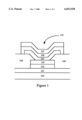
- FIG. 1 illustrates a cross-section of a typical antifuse 110 having a substrate 100, a first insulating layer 101 formed on substrate 100, and a first conductive layer 102 formed on first insulating layer 101.
- first conductive layer 102 includes aluminum.
- a first barrier metal layer 103 is formed and patterned on first conductive layer 102 (wherein first barrier metal layer 103 and first conductive layer 102 in combination are referred to as the bottom electrode).
- a second insulating layer 104 is deposited and etched to form a via to barrier metal layer 103.
- An amorphous silicon layer 105 is formed over second insulating layer 104 and first barrier metal layer 103.
- a second barrier metal layer 106 as well as a second conductive layer 107 are formed on amorphous silicon layer 105 (wherein second barrier metal layer 106 and second conductive layer 107 in combination are referred to as the top electrode).
- a conductive link (not shown) is formed between first barrier metal layer 103 and second barrier metal layer 106 by applying a positive voltage to either the top or the bottom electrode (referenced herein as the positive electrode).
- the electrode not receiving the positive voltage i.e. the negative electrode
- barrier metal layers 103 and 106 prevent the interdiffusion of the aluminum with the silicon in amorphous silicon layer 105.
- this conductive link has an associated resistance. Typically, this resistance increases somewhat over time. This phenomena is referred to herein as R on aging. If the resistance is too high, the functioning of the antifuse may be adversely affected, even resulting in failure. In a programmable logic device, the failure of one antifuse may be disastrous since the programmed circuit may no longer be realized in the integrated circuit. Thus, a goal of any antifuse process is to improve R on aging as much as possible. Therefore, a need arises to provide a method of improving R on aging, thereby ensuring greater on-state reliability of the antifuses.
- the interface between the positive electrode (during programming) and the amorphous silicon layer of the antifuse is treated, thereby resulting in significantly improved on-state reliability.
- Treatments of the present invention include, but are not limited to, a plasma etch using carbon tetrafluoride (CF 4 ), a sputter clean using Argon, and wet chemical treatments using dimethyl formamide (and water) or a resist developer.
- FIG. 1 illustrates a cross-section of a typical antifuse.
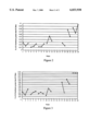
- FIG. 2 is a graph showing the resistance distribution of multiple wafers of the present invention after 4 minutes.
- FIG. 3 is a graph showing the resistance distribution of multiple wafers of the present invention after 2 weeks.
- cleaning the bottom electrode interface (i.e. the top of first conductive layer 102) of the antifuse before amorphous silicon deposition improves the R on aging and thus the on-state reliability of the antifuse.
- cleaning the top electrode interface (i.e. the top of amorphous silicon layer 105) before deposition of barrier metal layer 106 improves the R onaging and thus the on-state reliability of the antifuse.
- a thin layer of oxide and organic material at the positive electrode interface prevents the conductive link from making a good weld with the positive electrode. This bad weld can result in a resistance increase over time as the conductive link becomes disconnected from the positive electrode.
- the acceptable range of resistance for any antifuse is determined by its application. For example, an antifuse in a high speed path must have a lower resistance relative to another antifuse in a low speed path.
- 100% of the antifuses on a chip exhibit a resistance between 40-60 Ohms. Over time, sometimes in a matter of minutes, less than 100% of the antifuses exhibit this same resistance range. Due to the statistical nature of the use of antifuses in circuit applications, a certain percentage of R on aging may be acceptable. However, a much higher resistance, such as over 1000 Ohms can cause an circuit malfunction, once again depending on the application.
- antifuses having measured resistances greater than 80 Ohms were selected. Note that this resistance range is at least 20 Ohms higher than the initially programmed resistance range.
- FIGS. 2 and 3 show the percentage of resistance distribution for various wafers (having bottom electrode treatments) greater than 80 Ohms after four minutes and two weeks, respectively, after programming (wherein the bottom electrode was the positive electrode during programming). Note again that directly after programming, no antifuses have resistances greater than 60 Ohms.
- Illustrative bottom electrode interface treatments for various wafers are summarized in Table 1 below.
- TCA refers to a plasma etch done with a TCA Etcher manufactured by Tokyo Ohka Kogyo Ltd.
- ILC 1051 refers to a sputter clean done with an Anelva 1051 Etcher
- C30 refers to any known resist developer (including one by the brand name C30).
- An illustrative top electrode (wherein the top electrode is the positive electrode during programming) interface treatment includes, but is not limited to, a sputter clean using Argon under the conditions indicated above in Table 1.
- treating the positive electrode interfaces of the antifuses results in a lower percentage of resistance distribution greater than 80 Ohms. In accordance with some treatments, this improvement is actually on an order of magnitude. Because the present invention reduces the R on aging compared to the prior art in which no treatment of the positive electrode is performed, it logically follows that the present invention also improves on-state reliability of the antifuses.
Abstract
Treatment of the positive electrode interface of an antifuse provides significantly improved on-state reliability. Treatments include, but are not limited to, a plasma etch using carbon tetrafluoride (CF4), a sputter clean using Argon, and wet chemical treatments using dimethyl formamide (and water) or a resist developer.
Description
1. Field of the Invention
The present invention relates to an antifuse, and particularly to an antifuse which improves on-state reliability.
2. Description of the Related Art
Antifuses are well known in the art of programmable logic devices. An antifuse is a structure which is non-conductive when manufactured, but becomes permanently conductive by applying a predetermined voltage across its terminals (i.e. programming the antifuse). Antifuses are typically used in programmable logic devices to programmably interconnect conductive lines.
FIG. 1 illustrates a cross-section of a typical antifuse 110 having a substrate 100, a first insulating layer 101 formed on substrate 100, and a first conductive layer 102 formed on first insulating layer 101. Typically, first conductive layer 102 includes aluminum. A first barrier metal layer 103 is formed and patterned on first conductive layer 102 (wherein first barrier metal layer 103 and first conductive layer 102 in combination are referred to as the bottom electrode). A second insulating layer 104 is deposited and etched to form a via to barrier metal layer 103. An amorphous silicon layer 105 is formed over second insulating layer 104 and first barrier metal layer 103. A second barrier metal layer 106 as well as a second conductive layer 107 are formed on amorphous silicon layer 105 (wherein second barrier metal layer 106 and second conductive layer 107 in combination are referred to as the top electrode).
During programming, a conductive link (not shown) is formed between first barrier metal layer 103 and second barrier metal layer 106 by applying a positive voltage to either the top or the bottom electrode (referenced herein as the positive electrode). The electrode not receiving the positive voltage (i.e. the negative electrode) becomes heated and melts the associated barrier metal layer through the amorphous silicon layer, thereby forming the conductive link. For additional information regarding the formation of the conductive link, see "Antifuse Reliability and Link Formation Models", A. Iranmanesh et al., 1994 International Integrated Reliability Workshop Final Report, IEEE, which is incorporated herein by reference. Note that barrier metal layers 103 and 106 prevent the interdiffusion of the aluminum with the silicon in amorphous silicon layer 105.
As known by those skilled in the art, this conductive link has an associated resistance. Typically, this resistance increases somewhat over time. This phenomena is referred to herein as Ron aging. If the resistance is too high, the functioning of the antifuse may be adversely affected, even resulting in failure. In a programmable logic device, the failure of one antifuse may be disastrous since the programmed circuit may no longer be realized in the integrated circuit. Thus, a goal of any antifuse process is to improve Ron aging as much as possible. Therefore, a need arises to provide a method of improving Ron aging, thereby ensuring greater on-state reliability of the antifuses.
In accordance with the present invention, the interface between the positive electrode (during programming) and the amorphous silicon layer of the antifuse is treated, thereby resulting in significantly improved on-state reliability. Treatments of the present invention include, but are not limited to, a plasma etch using carbon tetrafluoride (CF4), a sputter clean using Argon, and wet chemical treatments using dimethyl formamide (and water) or a resist developer.
FIG. 1 illustrates a cross-section of a typical antifuse.
FIG. 2 is a graph showing the resistance distribution of multiple wafers of the present invention after 4 minutes.
FIG. 3 is a graph showing the resistance distribution of multiple wafers of the present invention after 2 weeks.
In accordance with one embodiment of the present invention in which the positive electrode is the bottom electrode, cleaning the bottom electrode interface (i.e. the top of first conductive layer 102) of the antifuse before amorphous silicon deposition improves the Ron aging and thus the on-state reliability of the antifuse. In another embodiment of the present invention in which the positive electrode is the top electrode, cleaning the top electrode interface (i.e. the top of amorphous silicon layer 105) before deposition of barrier metal layer 106 improves the Ronaging and thus the on-state reliability of the antifuse.
During programming of a typical antifuse, a thin layer of oxide and organic material at the positive electrode interface prevents the conductive link from making a good weld with the positive electrode. This bad weld can result in a resistance increase over time as the conductive link becomes disconnected from the positive electrode.
The acceptable range of resistance for any antifuse is determined by its application. For example, an antifuse in a high speed path must have a lower resistance relative to another antifuse in a low speed path. By careful design of the programming circuitry and algorithms, immediately after programming, 100% of the antifuses on a chip exhibit a resistance between 40-60 Ohms. Over time, sometimes in a matter of minutes, less than 100% of the antifuses exhibit this same resistance range. Due to the statistical nature of the use of antifuses in circuit applications, a certain percentage of Ron aging may be acceptable. However, a much higher resistance, such as over 1000 Ohms can cause an circuit malfunction, once again depending on the application.
For purposes of evaluating the antifuses of the present invention, antifuses having measured resistances greater than 80 Ohms were selected. Note that this resistance range is at least 20 Ohms higher than the initially programmed resistance range. FIGS. 2 and 3 show the percentage of resistance distribution for various wafers (having bottom electrode treatments) greater than 80 Ohms after four minutes and two weeks, respectively, after programming (wherein the bottom electrode was the positive electrode during programming). Note again that directly after programming, no antifuses have resistances greater than 60 Ohms. Illustrative bottom electrode interface treatments for various wafers are summarized in Table 1 below.
              TABLE 1
______________________________________
Wafers      Bottom Electrode Treatments
______________________________________
1, 2, 3     CF.sub.4 10 sccm, 250 W, 4.5 sec (TCA)
4, 5, 6             CF.sub.4 10 sccm, 250 W, 6.5 sec (TCA)
7, 8, 9             CF.sub.4 10 sccm, 250 W, 8.5 sec (TCA)
10, 11, 12       Ar, 450 W, 103 sec (ILC 1051)
17, 19:             Dimethyl formamide + H.sub.2 O (wet treatment)
20, 21:             Resist Developer (C30) (wet treatment)
22, 23, 24       None
______________________________________
wherein TCA refers to a plasma etch done with a TCA Etcher manufactured by Tokyo Ohka Kogyo Ltd., ILC 1051 refers to a sputter clean done with an Anelva 1051 Etcher, and C30 refers to any known resist developer (including one by the brand name C30). An illustrative top electrode (wherein the top electrode is the positive electrode during programming) interface treatment includes, but is not limited to, a sputter clean using Argon under the conditions indicated above in Table 1.
As shown by comparing wafers 22, 23, and 24 with the other wafers, treating the positive electrode interfaces of the antifuses results in a lower percentage of resistance distribution greater than 80 Ohms. In accordance with some treatments, this improvement is actually on an order of magnitude. Because the present invention reduces the Ron aging compared to the prior art in which no treatment of the positive electrode is performed, it logically follows that the present invention also improves on-state reliability of the antifuses.
Although the present invention has been described in reference to an antifuse structure shown in FIG. 1, other antifuse structures are also possible. For example, other antifuse structures include those described in U.S. Pat. No. 5,475,253 and U.S. Ser. No. 08/672,185 which are incorporated by reference herein. Other embodiments, including other interface electrode treatments, will be apparent to those skilled in art in light of the specification. Those skilled in the art will also recognize that for bidirectional pulse programming the initial pulse determines which electrode is considered positive for purposes of this invention. Specifically, the electrode receiving the first positive voltage pulse is considered the positive electrode. The present invention is defined by the claims appended hereto.
Claims (11)
1. A method of improving on-state reliability of an antifuse consisting of the steps of:
forming a first conductive layer;
forming a barrier metal layer on said first conductive layer;
forming an amorphous silicon layer on said barrier metal layer;
forming a second conductive layer on said amorphous silicon layer,
wherein (1) if said first conductive layer is a positive electrode, then removing grown oxide on a bottom electrode interface and (2) if said second conductive layer is the positive electrode, then removing grown oxide on a top electrode interface.
2. The method of claim 1 wherein said removing for (1) includes using carbon tetrafloride (CF4).
3. The method of claim 1 wherein said removing includes Argon.
4. The method of claim 1 wherein said removing for (1) includes using dimethyl formamide.
5. The method of claim 1 wherein said grown oxide includes organic material.
6. A method of improving on-state reliability of an antifuse consisting of the steps of:
forming a first conductive layer
forming a barrier metal layer on said first conductive layer;
forming an amorphous silicon layer on said barrier metal layer; and
forming a second conductive layer on said amorphous silicon layer,
wherein (1) if said first conductive layer is a positive electrode, then removing grown oxide on a bottom electrode interface using a sputter clean using Argon and (2) if said second conductive layer is the positive electrode, then removing grown oxide on a top electrode interface using a sputter clean using Argon.
7. The method of claim 6 wherein said grown oxide includes organic material.
8. A method of improving on-state reliability of an antifuse consisting of the steps of:
forming a first conductive layer;
forming a barrier metal layer on said first conductive layer;
forming an amorphous silicon layer on said barrier metal layer; and
forming a second conductive layer on said amorphous silicon layer,
wherein (1) if said first conductive layer is a positive electrode, then cleaning a bottom electrode interface and (2) if said second conductive layer is the positive electrode, then cleaning a top electrode interface.
9. The method of claim 8, wherein said cleaning for (1) includes using carbon tetrafloride (CF4).
10. The method of claim 8, wherein said cleaning includes using Argon.
11. The method of claim 8 wherein said cleaning for (1) includes dimethyl formamide.
Priority Applications (1)
| Application Number | Priority Date | Filing Date | Title |
|---|---|---|---|
| US08/751,193 US6033938A (en) | 1996-11-15 | 1996-11-15 | Antifuse with improved on-state reliability |
Applications Claiming Priority (1)
| Application Number | Priority Date | Filing Date | Title |
|---|---|---|---|
| US08/751,193 US6033938A (en) | 1996-11-15 | 1996-11-15 | Antifuse with improved on-state reliability |
Publications (1)
| Publication Number | Publication Date |
|---|---|
| US6033938A true US6033938A (en) | 2000-03-07 |
Family
ID=25020903
Family Applications (1)
| Application Number | Title | Priority Date | Filing Date |
|---|---|---|---|
| US08/751,193 Expired - Lifetime US6033938A (en) | 1996-11-15 | 1996-11-15 | Antifuse with improved on-state reliability |
Country Status (1)
| Country | Link |
|---|---|
| US (1) | US6033938A (en) |
Cited By (2)
| Publication number | Priority date | Publication date | Assignee | Title |
|---|---|---|---|---|
| US6362023B1 (en) * | 1998-08-17 | 2002-03-26 | National Semiconductor Corporation | Dielectric-based anti-fuse cell with polysilicon contact plug and method for its manufacture |
| US20060094197A1 (en) * | 2004-11-04 | 2006-05-04 | Bomy Chen | Method of trimming semiconductor elements with electrical resistance feedback |
Citations (9)
| Publication number | Priority date | Publication date | Assignee | Title |
|---|---|---|---|---|
| US4456679A (en) * | 1982-08-21 | 1984-06-26 | Basf Aktiengesellschaft | Production of relief images or resist images by a positive-working method |
| US5322812A (en) * | 1991-03-20 | 1994-06-21 | Crosspoint Solutions, Inc. | Improved method of fabricating antifuses in an integrated circuit device and resulting structure |
| US5399527A (en) * | 1992-03-28 | 1995-03-21 | Yamaha Corporation | Method of forming multilayer aluminum wiring in semiconductor IC |
| US5475253A (en) * | 1992-08-21 | 1995-12-12 | Xilinx, Inc. | Antifuse structure with increased breakdown at edges |
| US5484746A (en) * | 1989-09-07 | 1996-01-16 | Canon Kabushiki Kaisha | Process for forming semiconductor thin film |
| US5543656A (en) * | 1990-04-12 | 1996-08-06 | Actel Corporation | Metal to metal antifuse |
| US5565702A (en) * | 1994-08-19 | 1996-10-15 | Kawasaki Steel Corporation | Antifuse element, semiconductor device having antifuse elements, and method for manufacturing the same |
| US5633194A (en) * | 1995-04-18 | 1997-05-27 | The University Of Waterloo | Low temperature ion-beam assisted deposition methods for realizing SiGe/Si heterostructure |
| US5786240A (en) * | 1996-06-27 | 1998-07-28 | Xilinx, Inc. | Method for over-etching to improve voltage distribution |
-
1996
- 1996-11-15 US US08/751,193 patent/US6033938A/en not_active Expired - Lifetime
Patent Citations (10)
| Publication number | Priority date | Publication date | Assignee | Title |
|---|---|---|---|---|
| US4456679A (en) * | 1982-08-21 | 1984-06-26 | Basf Aktiengesellschaft | Production of relief images or resist images by a positive-working method |
| US5484746A (en) * | 1989-09-07 | 1996-01-16 | Canon Kabushiki Kaisha | Process for forming semiconductor thin film |
| US5543656A (en) * | 1990-04-12 | 1996-08-06 | Actel Corporation | Metal to metal antifuse |
| US5322812A (en) * | 1991-03-20 | 1994-06-21 | Crosspoint Solutions, Inc. | Improved method of fabricating antifuses in an integrated circuit device and resulting structure |
| US5399527A (en) * | 1992-03-28 | 1995-03-21 | Yamaha Corporation | Method of forming multilayer aluminum wiring in semiconductor IC |
| US5475253A (en) * | 1992-08-21 | 1995-12-12 | Xilinx, Inc. | Antifuse structure with increased breakdown at edges |
| US5502000A (en) * | 1992-08-21 | 1996-03-26 | Xilinx, Inc. | Method of forming a antifuse structure with increased breakdown at edges |
| US5565702A (en) * | 1994-08-19 | 1996-10-15 | Kawasaki Steel Corporation | Antifuse element, semiconductor device having antifuse elements, and method for manufacturing the same |
| US5633194A (en) * | 1995-04-18 | 1997-05-27 | The University Of Waterloo | Low temperature ion-beam assisted deposition methods for realizing SiGe/Si heterostructure |
| US5786240A (en) * | 1996-06-27 | 1998-07-28 | Xilinx, Inc. | Method for over-etching to improve voltage distribution |
Non-Patent Citations (4)
| Title |
|---|
| Ali Iranmanesh, Yakov Karpovich, Sukyoon Yoon, "Antifuse Reliability and Link Formation Models", pp. 90-94, IEEE 1994 International Integrated Reliability Workshop Final Report, sponsored by IEEE Electron Devices Society and the IEEE Reliability Society, 1994. |
| Ali Iranmanesh, Yakov Karpovich, Sukyoon Yoon, Antifuse Reliability and Link Formation Models , pp. 90 94, IEEE 1994 International Integrated Reliability Workshop Final Report, sponsored by IEEE Electron Devices Society and the IEEE Reliability Society, 1994. * |
| Robert F. Pierret, "Ohmic Contacts", Semiconductor Device Fundamentals, School of Electrical and Computer Engineering, Purdue University, 1996, pp. 498-500. |
| Robert F. Pierret, Ohmic Contacts , Semiconductor Device Fundamentals, School of Electrical and Computer Engineering, Purdue University, 1996, pp. 498 500. * |
Cited By (5)
| Publication number | Priority date | Publication date | Assignee | Title |
|---|---|---|---|---|
| US6362023B1 (en) * | 1998-08-17 | 2002-03-26 | National Semiconductor Corporation | Dielectric-based anti-fuse cell with polysilicon contact plug and method for its manufacture |
| US20060094197A1 (en) * | 2004-11-04 | 2006-05-04 | Bomy Chen | Method of trimming semiconductor elements with electrical resistance feedback |
| US7351613B2 (en) * | 2004-11-04 | 2008-04-01 | Silicon Storage Technology, Inc. | Method of trimming semiconductor elements with electrical resistance feedback |
| US20080131982A1 (en) * | 2004-11-04 | 2008-06-05 | Bomy Chen | Method Of Trimming Semiconductor Elements With Electrical Resistance Feedback |
| US7790518B2 (en) | 2004-11-04 | 2010-09-07 | Silicon Storage Technology, Inc. | Method of trimming semiconductor elements with electrical resistance feedback |
Similar Documents
| Publication | Publication Date | Title |
|---|---|---|
| US5510629A (en) | Multilayer antifuse with intermediate spacer layer | |
| US7393722B1 (en) | Reprogrammable metal-to-metal antifuse employing carbon-containing antifuse material | |
| US7867832B2 (en) | Electrical fuse and method of making | |
| US5663091A (en) | Method for fabricating an electrically programmable antifuse | |
| US5449947A (en) | Read-disturb tolerant metal-to-metal antifuse and fabrication method | |
| US5248632A (en) | Method of forming an antifuse | |
| US5693556A (en) | Method of making an antifuse metal post structure | |
| US5759876A (en) | Method of making an antifuse structure using a metal cap layer | |
| WO1995023431A1 (en) | Antifuse with double via contact | |
| US5387311A (en) | Method for manufacturing anti-fuse structures | |
| WO1997016851A9 (en) | Antifuse structure and process for manufacturing the same | |
| US5447880A (en) | Method for forming an amorphous silicon programmable element | |
| US6265257B1 (en) | Method of making a barrier layer to protect programmable antifuse structure from damage during fabrication sequence | |
| US5652175A (en) | Method for manufacturing a fuse structure | |
| JPH0770600B2 (en) | How to modify an integrated circuit | |
| US6033938A (en) | Antifuse with improved on-state reliability | |
| US6156588A (en) | Method of forming anti-fuse structure | |
| US5658819A (en) | Antifuse structure and process for manufacturing the same | |
| US20030062592A1 (en) | Fuse element, semiconductor device and method for manufacturing the same | |
| EP0583119B1 (en) | Programmable contact structure | |
| US6159836A (en) | Method for forming programmable contact structure | |
| WO2005081976A9 (en) | Reprogrammable metal-to-metal antifuse employing carbon-containing antifuse material | |
| US6469363B1 (en) | Integrated circuit fuse, with focusing of current | |
| KR950010873B1 (en) | Semiconductor device | |
| DE10325290B4 (en) | A manufacturing method for forming a fuse for a semiconductor device |
Legal Events
| Date | Code | Title | Description |
|---|---|---|---|
| AS | Assignment |
Owner name: XILINX, INC., CALIFORNIA Free format text: ASSIGNMENT OF ASSIGNORS INTEREST;ASSIGNORS:VOOGEL, MARTIN L.;KARPOVICH, YAKOV;HART, MICHAEL J.;REEL/FRAME:008310/0171;SIGNING DATES FROM 19961114 TO 19961115 |
|
| STCF | Information on status: patent grant |
Free format text: PATENTED CASE |
|
| FPAY | Fee payment |
Year of fee payment: 4 |
|
| FPAY | Fee payment |
Year of fee payment: 8 |
|
| FPAY | Fee payment |
Year of fee payment: 12 |