US5986515A - Temperature compensation crystal oscillator - Google Patents
Temperature compensation crystal oscillator Download PDFInfo
- Publication number
- US5986515A US5986515A US09/006,931 US693198A US5986515A US 5986515 A US5986515 A US 5986515A US 693198 A US693198 A US 693198A US 5986515 A US5986515 A US 5986515A
- Authority
- US
- United States
- Prior art keywords
- temperature
- crystal
- frequency varying
- crystal oscillator
- analog
- Prior art date
- Legal status (The legal status is an assumption and is not a legal conclusion. Google has not performed a legal analysis and makes no representation as to the accuracy of the status listed.)
- Expired - Fee Related
Links
- 239000013078 crystal Substances 0.000 title claims abstract description 181
- 238000012937 correction Methods 0.000 claims abstract description 72
- 230000001131 transforming effect Effects 0.000 claims abstract description 3
- 238000006243 chemical reaction Methods 0.000 claims description 37
- 230000004044 response Effects 0.000 claims description 12
- 238000010586 diagram Methods 0.000 description 9
- 230000009467 reduction Effects 0.000 description 9
- 239000003990 capacitor Substances 0.000 description 7
- 238000007689 inspection Methods 0.000 description 7
- 238000000034 method Methods 0.000 description 6
- 230000010355 oscillation Effects 0.000 description 6
- 230000002950 deficient Effects 0.000 description 5
- 230000001413 cellular effect Effects 0.000 description 4
- 238000004519 manufacturing process Methods 0.000 description 4
- 239000004065 semiconductor Substances 0.000 description 4
- 239000000470 constituent Substances 0.000 description 3
- 238000012545 processing Methods 0.000 description 3
- 238000010348 incorporation Methods 0.000 description 2
- 230000004888 barrier function Effects 0.000 description 1
- 239000012141 concentrate Substances 0.000 description 1
- 238000010276 construction Methods 0.000 description 1
- 238000011161 development Methods 0.000 description 1
- 230000000694 effects Effects 0.000 description 1
- 230000010354 integration Effects 0.000 description 1
- 238000012886 linear function Methods 0.000 description 1
- 239000000203 mixture Substances 0.000 description 1
- 229910021420 polycrystalline silicon Inorganic materials 0.000 description 1
- 230000008569 process Effects 0.000 description 1
- 230000002250 progressing effect Effects 0.000 description 1
- 238000007670 refining Methods 0.000 description 1
- 238000004904 shortening Methods 0.000 description 1
- 230000001360 synchronised effect Effects 0.000 description 1
Images


Classifications
-
- H—ELECTRICITY
- H03—ELECTRONIC CIRCUITRY
- H03B—GENERATION OF OSCILLATIONS, DIRECTLY OR BY FREQUENCY-CHANGING, BY CIRCUITS EMPLOYING ACTIVE ELEMENTS WHICH OPERATE IN A NON-SWITCHING MANNER; GENERATION OF NOISE BY SUCH CIRCUITS
- H03B5/00—Generation of oscillations using amplifier with regenerative feedback from output to input
- H03B5/02—Details
- H03B5/04—Modifications of generator to compensate for variations in physical values, e.g. power supply, load, temperature
-
- H—ELECTRICITY
- H03—ELECTRONIC CIRCUITRY
- H03L—AUTOMATIC CONTROL, STARTING, SYNCHRONISATION, OR STABILISATION OF GENERATORS OF ELECTRONIC OSCILLATIONS OR PULSES
- H03L1/00—Stabilisation of generator output against variations of physical values, e.g. power supply
- H03L1/02—Stabilisation of generator output against variations of physical values, e.g. power supply against variations of temperature only
- H03L1/028—Stabilisation of generator output against variations of physical values, e.g. power supply against variations of temperature only of generators comprising piezoelectric resonators
Definitions
- the present invention relates to a temperature compensated crystal oscillator for use in cellular phones and other small-scale electronic devices.
- the temperature compensated crystal oscillator uses as its oscillation source a 10 MHz range AT-cut crystal resonator (crystal unit), which cooperates with any frequency varying means to constitute a temperature compensating circuit thereby canceling the temperature characteristics depend on cubic finction of the AT-cut crystal resonator, to consequently stabilize the oscillating frequency.
- a 10 MHz range AT-cut crystal resonator crystal unit
- any frequency varying means to constitute a temperature compensating circuit thereby canceling the temperature characteristics depend on cubic finction of the AT-cut crystal resonator, to consequently stabilize the oscillating frequency.
- it is roughly classified into an analog temperature compensated crystal oscillator and a digital temperature compensated crystal oscillator.
- a one chip semiconductor integrated circuit has been used to make an analog temperature compensation crystal oscillator (hereinafter referred to as a one chip analog temperature compensated crystal oscillator), which is disclosed in Kuichi Kubo etc., "1996 IEEE INTERNATIONAL FREQUENCY CONTROL SYMPOSIUM" pp 728-734.
- composition of the one chip analog temperature compensated crystal oscillator and the method of adjusting the oscillating frequency basically resembles that for the digital temperature compensated crystal oscillator, with the result that their methods of cost reduction also resemble each other and lowering the cost of adjustment has become a crucial point.
- analog temperature compensated crystal oscillators compensate temperature by combining electronic parts that have different temperature characteristics, finding the optimum combination of parts and raising the percentage of obtaining passed products without changing the parts, has become a main concern.
- temperature compensated crystal oscillators having conventional configurations contain an intrinsic barrier to any real cost reduction.
- the analog temperature compensated crystal oscillators involve large parts costs and mounting costs due to too many constituent electronic parts. As well, the cost of refining and readjusting substandard products, found in the inspections at shipment, into passed products, is extremely high.
- the one chip analog compensated crystal oscillator appears to be superior to the digital temperature compensated crystal oscillator in that the integrating circuit is not necessary, the process of writing of data is nearly the same as that of the digital temperature compensated crystal oscillator. Therefore, the task of lowering this cost is not progressing well.
- the current construction of the conventional temperature compensated crystal oscillator it is extremely difficult to achieve a substantial reduction in costs.
- the present invention was therefore conceived in order to solve the above problems with its object to reduce the costs of the temperature compensated crystal oscillators.
- the temperature characteristics of all crystal resonators can be substantially represented by a single cubic curve, by shifting the absolute values of the oscillating frequencies in the direction of the ordinate axis so as to allow all the cubic curves to concentrate at a reference temperature (usually 25° C. in the case of crystal resonators for communications; this step is referred to as f0 adjustment) and by performing at each temperature a correction of the frequency deviation proportional to the difference in temperature relative to the reference temperature to make the gradient of the cubic curve substantially null in the vicinity of the reference temperature (this step is referred to as a gradient correction).
- Such superposition of temperature characteristic curves of the oscillating frequencies having various initial characteristics ensures that if the f0 adjustment and the gradient correction are merely performed depending on the unevenness of the manufacture of the crystal resonators, then the remaining correction, that is, the correction for linearizing the superposed cubic curve (this step is referred to as the linearizing correction) can be effected merely by using a coefficient common to all crystal resonators.
- a temperature compensated crystal oscillator in accordance with the present invention comprises a crystal oscillation means having an AT-cut crystal resonator; a linearizing correction means for transforming a temperature characteristic curve of an oscillating frequency of the crystal resonator into a straight line using a fixed coefficient common to all crystal resonators; a gradient correction means for eliminating a gradient of the linearized temperature characteristic of the oscillating frequency using a variable coefficient depending on the type of crystal resonator; and an f0 adjustment means for adjusting the gradient corrected temperature characteristic of the oscillating frequency so as to cause the oscillating frequency to lie within an allowable range.
- This configuration enables the temperature compensation to be divided into a linearizing correction, a gradient correction and an f0 adjustment, thereby extremely simplifying the adjustment of the oscillating frequency of the crystal resonator.
- the linearizing correction does not need any adjustment since it is common to all such crystal resonators, and the temperature characteristic curve of the oscillating frequency is linearized through this correction, so that the coefficient for the gradient correction can be obtained using only the temperature information on two different points.
- the f0 adjustment is carried out at a reference temperature, so that by employing one of the temperatures at the two different points as the reference temperature, the temperature information of only one point besides the reference temperature has only to be used to complete the adjustment of the temperature compensated crystal oscillator.
- the temperature compensated crystal oscillator in accordance with the present invention is able to reduce the adjustment costs for temperature compensation to a large extent as compared with the conventional digital temperature compensated crystal oscillator requiring temperature information of at least four points to obtain a cubic curve of the crystal resonator.
- the present invention is capable of shortening the time taken for the adjustment of the oscillating frequency (the temperature compensation), making it possible to achieve a lowered price for the temperature compensated crystal oscillator.
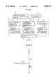
- FIG. 1 is a block diagram showing a configuration of a temperature compensated crystal oscillator in accordance with the first embodiment of the present invention
- FIG. 2 is a circuit diagram showing an example of the configuration of a variable capacitance circuit in FIG. 1;
- FIG. 3 is a circuit diagram showing an example of the configuration of a variable conversion coefficient analog converter in FIG. 1;
- FIG. 4 is a block diagram showing a configuration of a temperature compensated crystal oscillator in accordance with the second embodiment of the present invention.
- FIGS. 5 and 6 are graphic representations for explaining a temperature compensation adjustment in the second embodiment shown in FIG. 4;
- FIG. 7 is a block diagram showing a configuration of a temperature compensated crystal oscillator in accordance with the third embodiment of the present invention.
- FIG. 8 is a graph of the temperature characteristics versus oscillation frequencies of three crystal oscillators.
- FIG. 9 is a graph of the curves of FIG. 8 subjected to synchronization
- FIG. 10 is a graph of the curves of FIG. 9 subjected to linearizing correction
- FIG. 11 is a graph of the curves of FIG. 10 with their different gradients removed.
- FIG. 12 is a graph of the curves of FIG. 11 subjected to an f0 adjustment.
- FIG. 8 is a graphic representation of the temperature characteristics of the oscillating frequency of plural crystal oscillators A, B and C, which are respectively indicated by circular, triangular and square plots.
- the crystal oscillators Due to the temperature characteristics of their respective AT-cut crystal resonators, as shown in FIG. 8, the crystal oscillators have oscillating frequencies presenting different temperature characteristics expressed by cubic curves.
- the cubic curves of these characteristics are different from one another, they merely have different rotational angles relative to the frequency axis and the temperature axis, with their profiles being substantially the same.
- the cubic curves therefore coincide with one another, as shown in FIG. 9, if their rotational angles are corrected so as to be synchronized. This can be considered as being due to temperature characteristics intrinsic to the AT-cut crystal resonators (hereinafter, referred to as basic temperature characteristics), independent of any manufacturing differences or errors.
- compensation for the temperature characteristics of each crystal oscillator includes the compensation for the basic temperature characteristics shown in FIG. 9, the compensation for the rotational angle thereof, and f0 adjustment.
- a linearizing correction is first carried out using a fixed coefficient for linearizing the basic temperature characteristics shown in FIG. 9.
- the characteristic curves of the crystal oscillators A, B and C shown in FIG. 8 result in straight lines having different gradients as shown in FIG. 10.
- the straight lines in the case of the linearizing correction do not mean mathematically perfect straight lines but mean linear belts having widths of frequency deviation allowable as those of the temperature compensated crystal oscillators, they are illustrated as straight lines for convenience in the embodiments of the present invention and drawings.
- the crystal oscillators A, B and C are then subjected to a gradient correction for eliminating the respective gradients using different coefficients.
- the characteristic lines of the crystal oscillators A, B and C shown in FIG. 10 result in straight lines parallel to the temperature axis with no gradients, but with different oscillating frequencies, as shown in FIG. 11.
- An adjustment (f0 adjustment) is then performed for frequency deviation so as to cause the characteristics of the crystal oscillators A, B and C shown in FIG. 11 to lie within a desired oscillating frequency range.
- the crystal oscillators shown in FIG. 11 can obtain oscillations within the desired oscillating frequency range, independent of the temperature, as shown in FIG. 12.
- each crystal oscillator has been subjected to compensation in which the cubic curve indicative of the oscillating frequency vs. temperature characteristics as shown in FIG. 8 is processed intact, so that a larger compensation circuit and excessive labor time for the compensating adjustment is required, resulting in increased production costs.
- the temperature compensation for the oscillation frequency consists separately of the linearizing correction, gradient correction and f0 adjustment as herein described, so that the linearizing correction is fixed and need not be altered, with the actually performed gradient correction being a processing conscious of the linear curve, and with the f0 adjustment being mere processing at the temperature at a certain reference point, thus making it possible to reduce the size of the compensation circuit as compared with the conventional compensation in which the cubic curve is directly processed, as well as ensuring a simple compensation adjustment, contributing to a significant reduction in production costs.
- the temperature compensated crystal oscillator comprises, as shown in FIG. 1, crystal oscillating means 1 having an AT-cut crystal resonator; a non-volatile memory 2 storing therein gradient information on the temperature characteristics of the AT-cut crystal resonator and f0 adjustment information; an analog voltage output temperature sensor 3 for providing in the form of analog signals the temperature information on the AT-cut crystal resonator; and first frequency varying means 4, second frequency varying means 5 and third frequency varying means 6, which are connected in parallel with the crystal oscillating means 1.
- the first frequency varying means 4 includes a fixed conversion coefficient analog converter (a first analog converter) 7 which converts the output voltage of the analog voltage output temperature sensor 3 into an other voltage with a fixed conversion coefficient, and a variable capacitance circuit (a first variable capacitance circuit ) 10A which varies the capacitance of the crystal oscillating means 1 in response to the output signals from the analog converter 7.
- a fixed conversion coefficient analog converter a first analog converter
- a variable capacitance circuit a first variable capacitance circuit 10A which varies the capacitance of the crystal oscillating means 1 in response to the output signals from the analog converter 7.
- the first frequency varying means 4 serves as linearizing correction means for carrying out the linearizing correction for approximating to a single straight line the cubic curve indicative of the temperature characteristics of the AT-cut crystal resonator, with the analog converter 7 serving as an inverted cubic curve generating circuit for generating an inverted cubic curve as a result of inversion of the cubic curve or serving as an inverted cubic curve line-approximation generating circuit.
- variable capacitance circuit 10A includes, as shown in FIG. 2 for instance, a variable capacitance element C1 and a DC cut capacitor C2 which are connected in series, with the series connection acting as a load for the crystal oscillating means 1 and being grounded.
- a control signal B from the analog converter 7 for instance is applied through an input resistor R1 to a connection point between the variable capacitance element C1 and the capacitor C2.
- variable capacitance circuit Although a very typical example of the variable capacitance circuit is illustrated in FIG. 2, the elements are subjected to some restrictions for use in the temperature compensated crystal oscillator.
- variable capacitance element C1 can be any element as long as it is of a voltage controlled type, but preferably it is a MOS capacitor in view of its easy incorporation into a semiconductor integrated circuit. Furthermore, although the variable capacitance circuit is connected to ground in the example shown in FIG. 2, it may be connected to any potential that ensures, a large variable width of the capacitance values since any DC potential at the object to be connected is ignored.
- the DC cut capacitor C2 is preferably a voltage independent capacitor, but this condition is not essential if it has a larger capacitance value than that of the variable capacitance element C1. Instead, in order not to reduce the variable width of the capacitance value of the variable capacitance element C1, a significant condition is that its stray capacitance must be extremely small.
- the input resistor R1 can be of the order of 1 M Q .
- a diffused resistor or a MOS resistor is not preferred since use of such an element having a large stray capacitance causes a reduction in the variable width of the capacitance value of the variable capacitance element C1.
- a polycrystalline silicon resistor is most preferred.
- the second frequency varying means 5 serve as gradient correction means for correcting the gradient of the temperature characteristics of the AT-cut crystal resonator, which has been subjected to the linearizing correction by the first frequency varying means 4.
- the second frequency varying means 5 includes a variable conversion coefficient analog converter (a second analog converter) 8 for converting an output voltage of the analog voltage output temperature sensor 3 into another voltage with the conversion coefficient varied, on the basis of gradient correction information stored in the non-volatile memory 2; and a variable capacitance circuit (a second variable capacitance circuit) 10B which varies the capacitance of the crystal oscillating means 1 in response to an output signal of the analog converter 8.
- the analog converter 8 consists, as shown in FIG. 3 for instance, of a series connection of a first p-channel MOS transistor T1 and a first n-channel MOS transistor T3, of a series connection of a second p-channel MOS transistor T2 and a second n-channel MOS transistor T4, and of a series connection of a resistor train 30 including a plurality of resistors which are connected in series and a third n-channel MOS transistor T5, with the three series connections being connected in parallel between the power source and ground.
- the gate of the first n-channel MOS transistor T3 is connected to both the gate and drain of the second n-channel MOS transistor T4, with the gate of the third n-channel MOS transistor T5 being connected to the drain of the first p-channel MOS transistor T1.
- connection points between the adjacent resistors of the resistor train 30 are a group of switches 31 whose opening and closing actions are controlled by a control signal C from the non-volatile memory 2 and whose other ends are connected together to provide a control signal B to the variable capacitance circuit 10B.
- the gate of the first p-channel MOS transistor T1 receives a signal A from the analog voltage output temperature sensor 3.
- the gate of the second p-channel MOS transistor T2 is connected to one of the connection points between the adjacent resistors of the resistor train 30.
- variable conversion coefficient analog converter 8 shown in FIG. 3 is in the form of a forward amplifying circuit using a CMOS operational amplifier by way of example and is able to vary the conversion coefficient used when converting signal A from the analog voltage output temperature sensor 3 into a control signal B to be fed to the variable capacitance circuit 10B, by changing over the switches to the closed state in response to a control signal C from the non-volatile memory 2.
- variable conversion coefficient analog converter 8 is not limited to a forward amplifying circuit and that an inversion amplifying circuit is also available if an inverted signal of the signal A from the analog voltage output temperature sensor 3 is required as the control signal B to be fed to the variable capacitance circuit 10B.
- the inversion amplifying circuit is also able to vary the conversion coefficient.
- switches 31 are depicted as mechanical switches for the simplicity of representation, they actually are comprised of CMOS switches for example due to being incorporated into the semiconductor integrated circuit.
- variable conversion coefficient analog converter 8 An example of the variable conversion coefficient analog converter 8 has been hereinabove described with reference to FIG. 3. In respect to the fixed conversion coefficient analog converter 7 shown in FIG. 1, the illustration and description of a specific circuit example will be omitted since the group of switches 31 have only to be excluded from the variable conversion coefficient analog converter 8.
- the third frequency varying means 6 in FIG. 1 serve as f0 adjustment means for performing the f0 adjustment (the adjustment for causing the oscillating frequency deviation of the crystal oscillating circuit 1 to lie within a predetermined width) of the AT-cut crystal resonator temperature characteristics whose gradient is corrected by the second frequency varying means 5.
- the third frequency varying means 6 includes a D/A converter 9 for converting the f0 adjustment information output from the non-volatile memory 2 into an analog voltage, and a variable capacitance circuit (a third variable capacitance circuit) 10C for varying the capacitance of the crystal oscillating means 1 in response to an output signal from the D/A converter 9.
- signals for the linearizing correction are generated by the fixed conversion coefficient analog converter 7 so that there is no need to perform any adjustment for the linearizing correction after the assembly of the temperature compensated crystal oscillator, thus achieving zero adjustment cost.
- the two points may have any temperature, it is preferred that the temperature at one point normally be 25° C. with the other point having any arbitrary temperature, since the f0 adjustment is effected at the reference temperature of 25° C.
- this temperature compensated crystal oscillator completes all the adjutants by use of temperature information from only two points. That is, the non-volatile memory 2 has only to store the gradient correction information and the f0 adjustment information in conformity with the temperature information from two points.
- the temperature compensated crystal oscillator of the present invention needs a larger adjustment cost as compared with the conventional analog temperature compensated crystal oscillator requiring only the f0 adjustment after assembly.
- the analog temperature compensated crystal oscillator actually needs substantially the same cost as that of the gradient compensation means of the temperature compensated crystal oscillator of this embodiment in the step of selecting components before the assembly.
- this temperature compensated crystal oscillator and the conventional analog temperature compensated crystal oscillator incur substantially the same adjustment costs prior to inspection at shipment.
- the conventional analog temperature compensated crystal oscillator incurs a substantial cost because of the replacement of soldered components, whereas with the temperature compensated crystal oscillator in accordance with the present invention, it is only necessary to rewrite the content of the gradient correction information and the f0 adjustment information stored in the non-volatile memory on the basis of data obtained through the inspection at shipment, thus incurring a very small or substantially no cost.
- the temperature compensated crystal oscillator of this embodiment can achieve a reduction in the adjustment cost as compared with the conventional analog temperature compensated crystal oscillator.
- control signals are not allowed to digitally sharply vary with variations of the temperature, since when obtaining control signals for the variable capacitance circuits 10B and 10C from the temperature information, in the case of the temperature compensated crystal oscillator as shown in FIG. 1, the analog voltage output temperature sensor 3 provides the temperature information as analog signal outputs, which in turn are converted into other analog signals by the fixed conversion coefficient analog converter 7 or the variable conversion coefficient analog converter 8, with the post-conversion analog signals being used intact as the control signals for the variable capacitance circuits 10B and 10C.
- this temperature compensated crystal oscillator does not need any integration circuit as in the digital temperature compensated crystal oscillator, making it possible to reduce the number of constituent parts.
- this temperature compensated crystal oscillator is able to realize a low price with a reduction in the mounting costs due to the reduced number of constituent components and simplified processing.
- the three frequency varying means are connected in parallel with the crystal oscillating means 1, which is a preferred connection in order to minimize the influence of each frequency varying means on the other frequency varying means, and hence any series connection is prohibited if it has no means for outputting the output signals of these three frequency varying means together without being affected by one another.
- the temperature compensated crystal oscillator of the second embodiment comprises, as shown in FIG. 4, the crystal oscillating means 1 consisting of the AT-cut crystal resonator; and first frequency varying means 14, the second frequency varying means 5 and the third frequency varying means 6, which are connected in parallel with the crystal oscillating means 1.
- the first frequency variable means 14 includes a plurality of fixed conversion coefficient analog converters (first analog converters) 7A, 7B, and a plurality of variable capacitance circuits (first variable capacitance circuits) 10A1, 10A2, with the capacitance values of these variable capacitance circuits 10A1, 10A2 being controlled by the analog converters 7A, 7B, respectively.
- the temperature compensated crystal oscillator of this second embodiment differs from that of the first embodiment shown in FIG. 1 in that the first frequency varying means 14 is provided including a plurality of variable capacitance circuits and accordingly the plurality of fixed conversion coefficient analog converters 7A, 7B are provided for the control of the associated variable capacitance circuits 10A1, 10A2.
- the difference lies in that the linearizing correction is not carried out by a single variable capacitance circuit 10A, but is effected by a plurality of variable capacitance circuits, 10A1, 10A2.
- the linearizing correction is a correction for approximating to a single straight line a cubic line which is centrosymmetric with respect to a point of inflection, and hence the correction can be performed in a centrosymmetric manner if the straight line is selected so as to pass through the point of inflection.
- the execution of the centrosymmetrical linearizing correction with respect to the point of inflection results in the fact that the directions of correction for linearization are opposite with respect to the point of inflection, and means that in order to realize such a correction using a single variable capacitance circuit, the output of the analog converter 7 for the control of the capacitance value is expected to act in an extremely complicated manner on the temperature.
- the thus acting analog converter 7 has an enlarged circuit scale and becomes complicated, so that it may be difficult to set an optimum conversion coefficient.
- the first frequency varying means 4 includes a plurality of variable capacitance circuits 10A1, 10A2, and a plurality of analog converters 7 for controlling the plurality of variable capacitance circuits 10A1, 10A2.
- the first frequency varying means in this embodiment divides the temperature range to be compensated into a plurality of segments, with the fixed conversion coefficient analog converter thereof consisting of a plurality of analog converters 7A, 7b which voltage convert the output voltage of the analog voltage output type temperature sensor 3 using conversion coefficients differing on a segment-by-segment basis within the temperature range.
- the first variable capacitance circuit consists of a plurality of variable capacitance circuits 10A, 10B which vary the capacitance of the crystal oscillating means 1 in response to the output signals of the plurality of analog converters 7A, 7B.
- the temperature range to be compensated is divided by way of example into two segments, that is, the high temperature side and the low temperature side with respect to the point of inflection of the cubic curve indicative of the temperature characteristics of the AT-cut crystal resonator, this is not intended to be limitative and it may be subdivided to achieve a more accurate linearizing correction.
- the cubic curve indicative of the temperature characteristics of the AT-cut crystal resonator may be divided into five predetermined temperature segments (1 to 5 in the diagram).
- five sets of analog converters (each having a different fixed conversion coefficient) and variable capacitance circuits are provided so as to separately perform the linearizing correction within the respective temperature segments, thereby achieving a more accurate linearizing correction.
- the temperature compensated crystal oscillator of the third embodiment comprises, as shown in FIG. 7, the crystal oscillating means 1 including the AT-cut crystal resonator; and the first frequency varying means 14, second frequency varying means 15 and the third frequency varying means 6, which are connected in parallel with the crystal oscillating means 1.
- the first frequency varying means 14 consist of a plurality of fixed conversion coefficient analog converters 7A, 7B which are connected in parallel, and a plurality of variable capacitance circuits 10A1, 10A2, with the capacitance values of the variable capacitance circuits 10A1, 10A2 being controlled by the analog converters 7A, 7B, respectively.
- the second frequency varying means 15 consists of a plurality of variable conversion coefficient analog converters 8A, 8B (second analog converters) which are connected in parallel, and a plurality of variable capacitance circuits (second variable capacitance circuits) 10B1, 10B2, with the capacitance values of the variable capacitance circuits 10B1, 10B2 being controlled by the analog converters 8A, 8B, respectively.
- the third frequency varying means 6 is the same as that of the first embodiment hereinabove described.
- the temperature compensated crystal oscillator of the third embodiment differs from the second embodiment shown in FIG. 4 in that the second frequency varying means 15 consists of a plurality of variable capacitance circuits and that there are correspondingly provided a plurality of variable conversion coefficient analog converters 8A, 8B in order to control the variable capacitance circuits 10B1, 10B2.
- the difference lies in that the gradient correction is carried out by a plurality of variable capacitance circuits 10B1, 10B2, not by a single variable capacitance circuit 10B.
- variable capacitance circuits within the second frequency variable means 5 is the easiest measure for applying separate gradient corrections on the high temperature side and the low temperature side with respect to the reference temperature.
- the third embodiment shown in FIG. 7 provides an effective configuration for allowing the frequency accuracy to lie within the standard even in a case where the AT-cut crystal resonator used as the oscillation source for the temperature compensated crystal oscillator presents a defective temperature characteristic curve.
- the adjustment costs for the gradient correction are substantially the same as in the first embodiment. This is due to the fact that the gradient correction is applied temporarily using the same values of the conversion coefficients of the plurality of variable conversion coefficient analog converters 8A, 8B in the same manner as in the first embodiment and, if the oscillating frequency in the temperature region on the opposite side deviates from the standard during inspection at shipment, the gradient correction coefficient on that temperature side has only to be altered on the basis of the data, an operation easily performed during shipping inspection.
- the second frequency varying means 15 consists of two sets of variable conversion coefficient analog converters and variable capacitance circuits, it may be comprised of three or more sets of analog converters and variable capacitance circuits so as to ensure a more accurate gradient correction.
- variable conversion coefficient analog converter 8 shown in FIG. 3 employs as its reference system the high potential side power source, that is, the Vcc side, but instead it may employ the ground side as its reference system.
- the frequency varying means arranged in the temperature compensated crystal oscillator are divided into the linearizing correction means, gradient correction means and f0 adjustment means, with the gradient correction coefficients being determined by only two points of temperature information at the reference temperature and an other temperature so as to make it possible to greatly reduce the time taken to adjust the temperature compensation of the oscillating frequency.
Abstract
Description
Claims (12)
Applications Claiming Priority (2)
| Application Number | Priority Date | Filing Date | Title |
|---|---|---|---|
| JP9-004479 | 1997-01-14 | ||
| JP447997 | 1997-01-14 |
Publications (1)
| Publication Number | Publication Date |
|---|---|
| US5986515A true US5986515A (en) | 1999-11-16 |
Family
ID=11585253
Family Applications (1)
| Application Number | Title | Priority Date | Filing Date |
|---|---|---|---|
| US09/006,931 Expired - Fee Related US5986515A (en) | 1997-01-14 | 1998-01-14 | Temperature compensation crystal oscillator |
Country Status (1)
| Country | Link |
|---|---|
| US (1) | US5986515A (en) |
Cited By (24)
| Publication number | Priority date | Publication date | Assignee | Title |
|---|---|---|---|---|
| US6603364B2 (en) | 2000-03-17 | 2003-08-05 | Asahi Kasei Microsystems Co., Ltd. | Temperature-compensated crystal oscillator and method of temperature compensation |
| US6819194B2 (en) * | 2001-04-11 | 2004-11-16 | Kyocera Wireless Corp. | Tunable voltage-controlled temperature-compensated crystal oscillator |
| US20040263411A1 (en) * | 2002-02-12 | 2004-12-30 | Jorge Fabrega-Sanchez | System and method for dual-band antenna matching |
| US20050002343A1 (en) * | 2003-06-02 | 2005-01-06 | Toncich Stanley S. | System and method for filtering time division multiple access telephone communications |
| US20060132254A1 (en) * | 2004-12-22 | 2006-06-22 | Micro Analog Systems Oy | Temperature compensated crystal oscillator |
| US7071776B2 (en) | 2001-10-22 | 2006-07-04 | Kyocera Wireless Corp. | Systems and methods for controlling output power in a communication device |
| US7154440B2 (en) | 2001-04-11 | 2006-12-26 | Kyocera Wireless Corp. | Phase array antenna using a constant-gain phase shifter |
| US7164329B2 (en) | 2001-04-11 | 2007-01-16 | Kyocera Wireless Corp. | Tunable phase shifer with a control signal generator responsive to DC offset in a mixed signal |
| US7174147B2 (en) | 2001-04-11 | 2007-02-06 | Kyocera Wireless Corp. | Bandpass filter with tunable resonator |
| US7176845B2 (en) | 2002-02-12 | 2007-02-13 | Kyocera Wireless Corp. | System and method for impedance matching an antenna to sub-bands in a communication band |
| US7184727B2 (en) | 2002-02-12 | 2007-02-27 | Kyocera Wireless Corp. | Full-duplex antenna system and method |
| US7199698B1 (en) | 2004-04-06 | 2007-04-03 | Analog Devices, Inc. | Digitally-controlled reference oscillators |
| US7221243B2 (en) | 2001-04-11 | 2007-05-22 | Kyocera Wireless Corp. | Apparatus and method for combining electrical signals |
| US7248845B2 (en) | 2004-07-09 | 2007-07-24 | Kyocera Wireless Corp. | Variable-loss transmitter and method of operation |
| US7394430B2 (en) | 2001-04-11 | 2008-07-01 | Kyocera Wireless Corp. | Wireless device reconfigurable radiation desensitivity bracket systems and methods |
| US7548762B2 (en) | 2005-11-30 | 2009-06-16 | Kyocera Corporation | Method for tuning a GPS antenna matching network |
| US7746292B2 (en) | 2001-04-11 | 2010-06-29 | Kyocera Wireless Corp. | Reconfigurable radiation desensitivity bracket systems and methods |
| US20130237022A1 (en) * | 2006-12-20 | 2013-09-12 | Spansion Llc | Method and apparatus for protection against process-induced charging |
| US20160109496A1 (en) * | 2014-10-20 | 2016-04-21 | Fujitsu Limited | Measurement method and measurement system |
| US20160277031A1 (en) * | 2015-03-16 | 2016-09-22 | Seiko Epson Corporation | Oscillator, Electronic Apparatus, and Moving Object |
| US9548744B2 (en) | 2014-08-18 | 2017-01-17 | Qualcomm Incorporated | Compensating for hysteretic characteristics of crystal oscillators |
| US9618399B1 (en) * | 2012-09-26 | 2017-04-11 | Analog Devices, Inc. | Frequency correction of oscillators and related apparatus and methods |
| US10823623B2 (en) | 2018-04-26 | 2020-11-03 | Samsung Electronics Co., Ltd | System and method for modeling and correcting frequency of quartz crystal oscillator |
| US11876485B1 (en) * | 2022-09-13 | 2024-01-16 | Txc Corporation | Oscillating device |
Citations (1)
| Publication number | Priority date | Publication date | Assignee | Title |
|---|---|---|---|---|
| US5757244A (en) * | 1996-02-23 | 1998-05-26 | Kyocera Corporation | Digital control type oscillation circuit of portable telephone, crystal resonator oscillation frequency calculating method, and outputfrequency correcting method |
-
1998
- 1998-01-14 US US09/006,931 patent/US5986515A/en not_active Expired - Fee Related
Patent Citations (1)
| Publication number | Priority date | Publication date | Assignee | Title |
|---|---|---|---|---|
| US5757244A (en) * | 1996-02-23 | 1998-05-26 | Kyocera Corporation | Digital control type oscillation circuit of portable telephone, crystal resonator oscillation frequency calculating method, and outputfrequency correcting method |
Non-Patent Citations (2)
| Title |
|---|
| 1996 IEEE International Frequency Control Symposium; Analog TCXO Using One Chip LSI For Mobile Communication; Kuichi Kubo and Shuji Shibuya, pp. 728 734. * |
| 1996 IEEE International Frequency Control Symposium; Analog TCXO Using One Chip LSI For Mobile Communication; Kuichi Kubo and Shuji Shibuya, pp. 728-734. |
Cited By (40)
| Publication number | Priority date | Publication date | Assignee | Title |
|---|---|---|---|---|
| DE10191096B4 (en) * | 2000-03-17 | 2006-04-20 | Asahi Kasei Microsystems Co., Ltd. | Temperature compensated crystal oscillator and method of performing temperature compensation |
| US6603364B2 (en) | 2000-03-17 | 2003-08-05 | Asahi Kasei Microsystems Co., Ltd. | Temperature-compensated crystal oscillator and method of temperature compensation |
| US7394430B2 (en) | 2001-04-11 | 2008-07-01 | Kyocera Wireless Corp. | Wireless device reconfigurable radiation desensitivity bracket systems and methods |
| US7221327B2 (en) | 2001-04-11 | 2007-05-22 | Kyocera Wireless Corp. | Tunable matching circuit |
| US7509100B2 (en) | 2001-04-11 | 2009-03-24 | Kyocera Wireless Corp. | Antenna interface unit |
| US7746292B2 (en) | 2001-04-11 | 2010-06-29 | Kyocera Wireless Corp. | Reconfigurable radiation desensitivity bracket systems and methods |
| US8237620B2 (en) | 2001-04-11 | 2012-08-07 | Kyocera Corporation | Reconfigurable radiation densensitivity bracket systems and methods |
| US7116954B2 (en) | 2001-04-11 | 2006-10-03 | Kyocera Wireless Corp. | Tunable bandpass filter and method thereof |
| US7154440B2 (en) | 2001-04-11 | 2006-12-26 | Kyocera Wireless Corp. | Phase array antenna using a constant-gain phase shifter |
| US7164329B2 (en) | 2001-04-11 | 2007-01-16 | Kyocera Wireless Corp. | Tunable phase shifer with a control signal generator responsive to DC offset in a mixed signal |
| US6819194B2 (en) * | 2001-04-11 | 2004-11-16 | Kyocera Wireless Corp. | Tunable voltage-controlled temperature-compensated crystal oscillator |
| US7174147B2 (en) | 2001-04-11 | 2007-02-06 | Kyocera Wireless Corp. | Bandpass filter with tunable resonator |
| US7265643B2 (en) | 2001-04-11 | 2007-09-04 | Kyocera Wireless Corp. | Tunable isolator |
| US7221243B2 (en) | 2001-04-11 | 2007-05-22 | Kyocera Wireless Corp. | Apparatus and method for combining electrical signals |
| US7071776B2 (en) | 2001-10-22 | 2006-07-04 | Kyocera Wireless Corp. | Systems and methods for controlling output power in a communication device |
| US7184727B2 (en) | 2002-02-12 | 2007-02-27 | Kyocera Wireless Corp. | Full-duplex antenna system and method |
| US7180467B2 (en) | 2002-02-12 | 2007-02-20 | Kyocera Wireless Corp. | System and method for dual-band antenna matching |
| US7176845B2 (en) | 2002-02-12 | 2007-02-13 | Kyocera Wireless Corp. | System and method for impedance matching an antenna to sub-bands in a communication band |
| US20040263411A1 (en) * | 2002-02-12 | 2004-12-30 | Jorge Fabrega-Sanchez | System and method for dual-band antenna matching |
| US7720443B2 (en) * | 2003-06-02 | 2010-05-18 | Kyocera Wireless Corp. | System and method for filtering time division multiple access telephone communications |
| US20050002343A1 (en) * | 2003-06-02 | 2005-01-06 | Toncich Stanley S. | System and method for filtering time division multiple access telephone communications |
| US8478205B2 (en) | 2003-06-02 | 2013-07-02 | Kyocera Corporation | System and method for filtering time division multiple access telephone communications |
| US7199698B1 (en) | 2004-04-06 | 2007-04-03 | Analog Devices, Inc. | Digitally-controlled reference oscillators |
| US7248845B2 (en) | 2004-07-09 | 2007-07-24 | Kyocera Wireless Corp. | Variable-loss transmitter and method of operation |
| US20060132254A1 (en) * | 2004-12-22 | 2006-06-22 | Micro Analog Systems Oy | Temperature compensated crystal oscillator |
| US7816993B2 (en) | 2004-12-22 | 2010-10-19 | Micro Analog System Oy | Temperature compensated crystal oscillator |
| US7403078B2 (en) * | 2004-12-22 | 2008-07-22 | Micro Analog System Oy | Temperature compensated crystal oscillator |
| US20080106348A1 (en) * | 2004-12-22 | 2008-05-08 | Micro Analog Systems Oy | Temperature compensated crystal oscillator |
| US7548762B2 (en) | 2005-11-30 | 2009-06-16 | Kyocera Corporation | Method for tuning a GPS antenna matching network |
| US9318373B2 (en) * | 2006-12-20 | 2016-04-19 | Cypress Semiconductor Corporation | Method and apparatus for protection against process-induced charging |
| US20130237022A1 (en) * | 2006-12-20 | 2013-09-12 | Spansion Llc | Method and apparatus for protection against process-induced charging |
| US9618399B1 (en) * | 2012-09-26 | 2017-04-11 | Analog Devices, Inc. | Frequency correction of oscillators and related apparatus and methods |
| US9548744B2 (en) | 2014-08-18 | 2017-01-17 | Qualcomm Incorporated | Compensating for hysteretic characteristics of crystal oscillators |
| US20160109496A1 (en) * | 2014-10-20 | 2016-04-21 | Fujitsu Limited | Measurement method and measurement system |
| US20160277031A1 (en) * | 2015-03-16 | 2016-09-22 | Seiko Epson Corporation | Oscillator, Electronic Apparatus, and Moving Object |
| CN105991128A (en) * | 2015-03-16 | 2016-10-05 | 精工爱普生株式会社 | Oscillator, electronic apparatus, and moving object |
| US10027331B2 (en) * | 2015-03-16 | 2018-07-17 | Seiko Epson Corporation | Oscillator, electronic apparatus, and moving object |
| US10823623B2 (en) | 2018-04-26 | 2020-11-03 | Samsung Electronics Co., Ltd | System and method for modeling and correcting frequency of quartz crystal oscillator |
| US10914643B2 (en) | 2018-04-26 | 2021-02-09 | Samsung Electronics Co., Ltd | System and method for modeling and correcting frequency of quartz crystal oscillator |
| US11876485B1 (en) * | 2022-09-13 | 2024-01-16 | Txc Corporation | Oscillating device |
Similar Documents
| Publication | Publication Date | Title |
|---|---|---|
| US5986515A (en) | Temperature compensation crystal oscillator | |
| US5473289A (en) | Temperature compensated crystal oscillator | |
| US7816993B2 (en) | Temperature compensated crystal oscillator | |
| US6294962B1 (en) | Circuit(s), architecture and method(s) for operating and/or tuning a ring oscillator | |
| US6362699B1 (en) | Temperature compensating circuit for a crystal oscillator | |
| US20070075797A1 (en) | Method of manufacturing crystal oscillator and the crystal oscillator manufactured by the method | |
| US20080007363A1 (en) | Function generation circuit | |
| US7154351B2 (en) | Approximate n-th order function generating device and temperature compensation crystal oscillation circuit | |
| US20080100373A1 (en) | Bandwidth calibration of active filter | |
| US5999063A (en) | Temperature-compensated crystal oscillator using square-law converter circuits for lower and higher temperature sides | |
| US20060012445A1 (en) | Voltage controlled oscillator | |
| JPH10261919A (en) | Temperature compensation-type crystal oscillator | |
| JP2713214B2 (en) | Temperature compensation device for crystal oscillation circuit | |
| JPH09297623A (en) | Voltage and current regulator circuit | |
| CN112684824B (en) | Temperature control circuit, oscillation control circuit, and temperature control method | |
| JPH06276020A (en) | Temperature compensated crystal oscillator | |
| JP4011198B2 (en) | Temperature compensated crystal oscillator | |
| JPH09298422A (en) | Tco circuit | |
| JP2975411B2 (en) | Temperature compensated piezoelectric oscillator | |
| JP3911722B2 (en) | Analog / digital input / output switch circuit | |
| CN109921785A (en) | A kind of temperature-compensation circuit of crystal oscillator | |
| JP3058425B2 (en) | Temperature compensated oscillator | |
| JPH10256899A (en) | Non-adjustment voltage controlled oscillation circuit | |
| JP2008300977A (en) | Temperature compensation crystal oscillator and method for compensating temperature of oscillator | |
| JP2006222646A (en) | Temperature-compensated quartz-crystal oscillator |
Legal Events
| Date | Code | Title | Description |
|---|---|---|---|
| AS | Assignment |
Owner name: CITIZEN WATCH CO., LTD., JAPAN Free format text: ASSIGNMENT OF ASSIGNORS INTEREST;ASSIGNOR:SAKURAI, YASUHIRO;REEL/FRAME:009239/0349 Effective date: 19980520 |
|
| FEPP | Fee payment procedure |
Free format text: PAYOR NUMBER ASSIGNED (ORIGINAL EVENT CODE: ASPN); ENTITY STATUS OF PATENT OWNER: LARGE ENTITY |
|
| CC | Certificate of correction | ||
| FPAY | Fee payment |
Year of fee payment: 4 |
|
| FPAY | Fee payment |
Year of fee payment: 8 |
|
| AS | Assignment |
Owner name: CITIZEN HOLDINGS CO., LTD., JAPAN Free format text: CHANGE OF NAME;ASSIGNOR:CITIZEN WATCH CO., LTD.;REEL/FRAME:019817/0701 Effective date: 20070402 |
|
| REMI | Maintenance fee reminder mailed | ||
| LAPS | Lapse for failure to pay maintenance fees | ||
| STCH | Information on status: patent discontinuation |
Free format text: PATENT EXPIRED DUE TO NONPAYMENT OF MAINTENANCE FEES UNDER 37 CFR 1.362 |
|
| FP | Lapsed due to failure to pay maintenance fee |
Effective date: 20111116 |