US5966004A - Electronic system with regulator, and method - Google Patents
Electronic system with regulator, and method Download PDFInfo
- Publication number
- US5966004A US5966004A US09/024,434 US2443498A US5966004A US 5966004 A US5966004 A US 5966004A US 2443498 A US2443498 A US 2443498A US 5966004 A US5966004 A US 5966004A
- Authority
- US
- United States
- Prior art keywords
- voltage
- transistor
- output node
- reference line
- comparator
- Prior art date
- Legal status (The legal status is an assumption and is not a legal conclusion. Google has not performed a legal analysis and makes no representation as to the accuracy of the status listed.)
- Expired - Fee Related
Links
Images


Classifications
-
- G—PHYSICS
- G05—CONTROLLING; REGULATING
- G05F—SYSTEMS FOR REGULATING ELECTRIC OR MAGNETIC VARIABLES
- G05F1/00—Automatic systems in which deviations of an electric quantity from one or more predetermined values are detected at the output of the system and fed back to a device within the system to restore the detected quantity to its predetermined value or values, i.e. retroactive systems
- G05F1/10—Regulating voltage or current
- G05F1/46—Regulating voltage or current wherein the variable actually regulated by the final control device is DC
- G05F1/618—Regulating voltage or current wherein the variable actually regulated by the final control device is DC using semiconductor devices in series and in parallel with the load as final control devices
-
- G—PHYSICS
- G05—CONTROLLING; REGULATING
- G05F—SYSTEMS FOR REGULATING ELECTRIC OR MAGNETIC VARIABLES
- G05F1/00—Automatic systems in which deviations of an electric quantity from one or more predetermined values are detected at the output of the system and fed back to a device within the system to restore the detected quantity to its predetermined value or values, i.e. retroactive systems
- G05F1/10—Regulating voltage or current
- G05F1/46—Regulating voltage or current wherein the variable actually regulated by the final control device is DC
- G05F1/56—Regulating voltage or current wherein the variable actually regulated by the final control device is DC using semiconductor devices in series with the load as final control devices
- G05F1/563—Regulating voltage or current wherein the variable actually regulated by the final control device is DC using semiconductor devices in series with the load as final control devices including two stages of regulation at least one of which is output level responsive, e.g. coarse and fine regulation
Definitions
- the present invention generally relates to electronic circuits, and more particularly, to an electronic system with regulator and to a method therefore.
- Many electronic system e.g., mobile phones
- regulators which couple supply devices (e.g., batteries, main transformers) and consuming devices (e.g., transmitters, speakers, logic circuits, memories).
- the properties of the regulators are described, for example, by an input voltage V IN , an input current I IN , an output voltage V OUT , and an output current I OUT .
- the regulator provides V OUT and I OUT within predetermined minimum and maximum values to the consuming device.
- a reverse action from the consuming device to the regulator is often not wanted but should be accommodated by the regulator.
- a regulator which uses energy effectively supplies V OUT and I OUT according to the needs the consuming components.
- the regulator receives V IN and I IN from a battery and provides V OUT and I OUT to a transmitter and to a memory.
- the transmitter sends radio signals in bursts (e.g., "operating mode A").
- the regulator should recover from changes of V OUT caused by the transmitter.
- the waiting time is crucial for the performance of the mobile phone.
- the regulator should consume only a low quiescent current (e.g., I IN ); and the output voltage V OUT should stay above a minimum value required by the memory.
- Regulators for such applications are known in the art as low-drop-out (LDO) regulators.
- the present invention seeks to provide regulators which mitigate or avoid disadvantages and limitations of the prior art.
- FIG. 1 illustrates a simplified circuit diagram of an electronic system according to the present invention
- FIGS. 2A and 2B illustrates the operation of a regulator of the system of FIG. 1 according to a method of the present invention by simplified time diagrams;
- FIGS. 3A and 3B illustrates the operation of a prior art regulator portion by simplified time diagrams
- FIG. 4 illustrates a simplified circuit diagram of the regulator according to a preferred embodiment of the present invention.
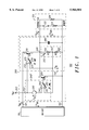
- FIG. 1 illustrates a simplified circuit diagram of electronic system 100 according to the present invention.
- Electronic system 100 comprises supply device 110, regulator 200 (dashed frame) and optional consuming device 120.
- supply device 110 can be a battery; and consuming device 120 can be the combination of a transmitter and a memory.
- Supply device 110 provides input voltage V IN to regulator 200 at reference lines 101 and 102.
- Input current I IN goes from supply device 110 to regulator 200 (illustrated on line 101).
- Regulator 200 provides output voltage V OUT between output node 205 and reference line 102 to consuming device 120.
- Consuming device 120 exhibits an inherent load between output node 205 and line 102.
- This load can be an ohmic resistance, a capacitance, an inductance or a combination therefrom.
- the load between node 205 and line 102 is represented by (a) serially coupled resistor 124 and switch 122 (e.g., the "transmitter") and (b) resistor 126 (e.g., the "memory").
- closed switch 122 means, for example, that the transmitter is operating and that consuming device 120 behaves like a current sink. When switch 122 opens, the current demand of the transmitter quickly decreases.
- the phrases “switch 122 closes” and “switch 122 opens” are intended to represent that the portion illustrated by resistor 124 (e.g., the "transmitter”) of consuming device 120 starts to operate and stops to operate, respectively.
- regulator 200 accommodates the load changes in an efficient way: Depending on the output voltage V OUT , regulator 200 switches node 205 to line 101 or to line 102. Details are explained later in the explanation of regulator 200 and of its preferred method of operation.
- Regulator 200 comprises voltage sensor 255 with resistors 250 and 260 for measuring V OUT , optional capacitor 280, comparators 230 and 240, switches 210 and 220, and voltage source 290.
- regulator 200 receives reference voltage V REF on optional terminal 203. This is convenient, but not essential for the present invention. Persons of skill in the art know how to provide V REF .
- V REF can be provided internally and can be derived from voltage V IN .
- Comparators 230 and 240 are, preferably, implemented by operational amplifiers (“op amps") wherein the terms “comparators” and “operational amplifiers” are used here as synonyms.
- Op amps 230 and 240 have non-inverting inputs 231 and 241, respectively, which are illustrated by the "+” symbol.
- op amps 230 and 240 have inverting inputs 232 and 242, respectively, with the "-" symbol. This input assignments are convenient for explaining the present invention but not limited thereto. Persons of skill in the art are able, based on the description herein, to modify op amps 230 and 240 and to implement regulator 200 in a different way without departing from the present invention.
- Switches 210 and 220 are, preferably, implemented by bipolar transistors (i.e., transistors 210 and 220).
- the term "transistor” is intended to include any component having at least two main electrodes and a control electrode. The impedance between the main electrodes (e.g., emitter E and collector C) is controlled by a signal applied to the control electrode (e.g., base B).
- the letters "E", "C” and “B” indicate the transistor electrodes.
- transistor 210 is a pnp-transistor (e.g., "first type") and transistor 220 is a npn-transistor (e.g., "second type”).
- First type and “second type” are intended to distinguish complementary transistors of opposite conductivity and can refer to either pnp-types or npn-types, as the case may be.
- complementary transistors 210 and 220 is convenient, but not essential for the present invention.
- transistors of equal type can also be used.
- transistors are able, based on the description herein, to use transistors in different configurations without departing from the scope of the present invention.
- the present invention is explained in connection with bipolar transistors, other transistor types (e.g., field effect transistors) are also useful.
- a "conductive" transistor is able to carry a current between its main electrodes; whereas a “non-conductive” transistor is substantially not able to carry a current.
- transistor 210 has larger physical dimensions (e.g., emitter areas) than transistor 220. In other words, transistor 210 can carry higher currents (i.e. I IN ) than transistor 220.
- op amp 240' (dashed frame) comprises op amp 240 and voltage source 290.
- Op amp 240' has inputs 241 and 242' (at terminal 203) parallel coupled to inputs 231 and 232 of op amp 230, respectively.
- Op amps 230 and 240' receive substantially the same input voltages (e.g., V REF and V M , explained later) and have different switching thresholds. In other words, there is an input offset voltage V OS between op amps 230 and 240.
- Voltage source 290 as shown in FIG. 1 is intended to illustrate any device which temporarily or substantially at all time can cause an offset voltage between its terminals.
- a device can be a resistor, a transistor, a diode, or a similar device.
- Persons of skill in the art are also able, based on the description herein, to provide a voltage drop by other means, such as by dimensioning the components of op amps 230 and 240, without departing from the scope of the present invention.
- a voltage offset between input stages of transistor amplifiers can be provided by different emitter areas.
- To associate voltage source 290 with op amp 240 is intended as a convenient example for explanation.
- a voltage source could also be associated with op amp 230.
- the components of regulator 200 are coupled as follows.
- the emitter (E) of transistor 210 is coupled to reference line 101.
- the collector (C) of transistor 210 is coupled to output node 205.
- Capacitor 280 is coupled between output node 205 and reference line 102.
- resistors 250 and 260 are serially coupled between output node 205 and reference line 102 via node 207.
- Resistor 250 has a value R 1 and resistor 260 has a value R 2 .
- the collector (C) of transistor 220 is coupled to output node 205; and the emitter (E) of transistor 220 is coupled to reference line 102.
- the base (B) of transistor 210 is coupled to output 235 of op amp 230.
- the base (B) of transistor 220 is coupled to output 245 of op amp 240.
- Input 231 of op amp 230 and input 241 of op amp 240 are coupled together to node 207.
- Input 232 of op amp 230 is coupled to terminal 203.
- Input 242 is coupled to terminal 203 via voltage source 290.
- the measurement voltage V M is the voltage across resistor 260
- the voltage V OS is the voltage of voltage source 290
- the current I R is the current through resistors 250 and 260.
- Regulator portion 150 is illustrated by dashed line 150 around voltage sensor 255, transistor 210, and op amp 230.
- FIGS. 2A and 2B illustrates the operation of regulator 200 of system 100 according to a method of the present invention by simplified time diagrams 310 and 320.
- (diagram 320) on vertical axes are related to time t on horizontal axes (diagrams 310 and 320).
- voltages and currents are considered in the following with their absolute values (symbols
- Regulator 200 alternatively operates in a first operating mode ("A-mode") when consuming device 120 of system 100 is active (e.g., transmitting radio signals in a burst) and in a second operating mode ("B-mode") when consuming device 120 is not active (e.g., waiting time between bursts, but supporting the memory).
- A-mode first operating mode
- B-mode second operating mode
- Transition time point t 1 marks the transition between the first mode and the second mode; and transition time point t 2 marks the transition between the second mode and the first mode.
- points t 1 and t 2 are intended to comprise the time intervals in which mode transitions are completed.
- dashed line 311 (parallel to the t-axis) indicates a minimum output voltage
- dashed line 312 (parallel to the t-axis) indicates a minimum output voltage
- the voltages are related as:
- is substantially smaller ( ⁇ ) than current
- Resistors 250 and 260 of voltage sensor 255 provide the measurement voltage
- Op amp 230 compares
- (trace 313) with an absolute value equal to ( ) or larger than (>)
- has a value of substantially
- Op amp 240 receives a voltage
- Op amp 240 controls transistor 220 to be substantially non-conductive.
- switch 122 opens and voltages
- at input 242 of op amp 240 remain substantially unchanged.
- Op amp 230 and 240 (having different thresholds) respond to the changing voltage
- transistor 220 When neglecting a current through resistor 126, transistor 220 does substantially not need to carry current
- Transistor 210 substantially interrupts the flow of current
- Transistor 220 discharges (trace 315) capacitor 280.
- is decreasing with the discharging so that op amp 240 makes transistor 220 non-conductive again.
- a delay occurs between switching off transistor 210 and switching on transistor 220.
- This is provided by op amps 230 and 240' with different switching thresholds (see difference
- input voltage
- input voltages
- the sink branch formed by transistor 220 between output node 205 and line 102 is active only during the load transient of time t 1 . At other times, this branch is not active, i.e. transistor 220 is substantially not conductive.
- transistor 220 remains substantially non-conductive so that there is no significant quiescent current through transistors 220.
- Transistor 210 conducts only the small current of resistor 126 (e.g., the memory) and the small current through resistors 250 and 260. This is an important advantage of the present invention and, for example, saves battery power.
- is at
- switch 122 closes.
- makes transistor 210 conductive and
- can temporarily drop ("undershooting", traces 317 and 318). During the drop,
- regulator 200 After t 2 (A-mode), regulator 200 operates similar as in the time before t 1 (traces 319 and 324).
- FIGS. 3A and 3B illustrates the operation of regulator portion 150 alone, by simplified time diagrams 410 (FIG. 3A) and 420 (FIG. 3B). Similar to FIG. 2, output voltage V OUT (diagram 410) and output current I OUT (diagram 420) on vertical axes are related to time t on horizontal axes (diagrams 410 and 420). Regulator portion 150 alone is used in the prior art. Regulator 150 operates in the first mode (A-mode) before t 1 and after t 2 and operates in the second mode (B-mode) between t 1 and t 2 . In diagram 410, dashed line 411 indicates V OUTA and dashed line indicates V OUTMIN .
- switch 122 Before t 1 (A-mode), switch 122 is closed. Transistor 210 is conductive and regulator portion 150 provides
- dashed traces 416' and 417' (at time t 2 ') for dropping voltage V OUT in diagram 410 and trace 424' (also at time t 2 ') for increasing current I OUT in diagram 420 are considered.
- Plain traces 416 and 417 in diagram 410 (drop) and plain trace 424 in diagram 420 are not considered.
- Trace 415 should be extended by dashed trace 415' and trace 423 should be extended by dashed trace 423'.
- the voltage shift by which V OUT temporarily drops during t 2 (see above (i) ) and t 2 ', depends on the magnitude of V OUT in the present discharging state. At time t 2 ' which is later than time t 2 , the load capacitance has been more discharged, that is:
- regulator 200 of the present invention discharges capacitor 280 faster than regulator portion 150 alone (prior art). Therefore, in regulator 200 of the invention,
- resistors 250 and 260 are used for a double purpose: (a) measuring V OUT and (b) discharging the load capacitance.
- the resistance values R 1 and R 2 should be, preferably, high (i.e. to keep quiescent current low) and for (b) discharging, R 1 and R 2 should be, preferably, low.
- the optimization of the resistor values determines (a) the power consumption of regulator portion 150 and (b) the discharge time or waiting time between t 1 and t 2 (or t 1 and t 2 ').
- this problems are solved by having different components for measuring (e.g., resistors 250 and 260) and components for discharging (e.g., transistors 220 and op amp 240). Waiting times are substantially reduced. This feature makes regulator 200 applicable for electronic systems in which consuming device 120 operates at high burst rates. The reduction of waiting times can also reduce software expenses.
- components for measuring e.g., resistors 250 and 260
- components for discharging e.g., transistors 220 and op amp 240.
- FIG. 4 illustrates a simplified circuit diagram of regulator 500 according to a preferred embodiment of the present invention.
- the following reference numbers correspond to analogous components or combinations thereof: 200/500, 101/501, 102/502, 203/503, 102/502, 203/503, 205/505, 207/507, 210/510, 230/530, 231/531, 232/532, 235/535, 240'/540', 241/541, 242'/542', 245/545, 250/550 and 260/560.
- their function can be different as a consequence of the embodiment of regulator 500.
- Regulator 500 comprises resistors 550, 560 and 590, current sources 582 and 584, pnp-transistors 510, 533, 536, 539, 543 and 546 and npn-transistors 520, 534, 537, 538, 544 and 547.
- Regulator 500 receives input voltage V IN between reference line 501 (the emitter of transistor 510) and reference line 502.
- Regulator 500 provides output voltage V OUT between output node 505 (the collector of transistor 510) and reference line 502.
- Regulator 500 also receives reference voltage V REF at terminal 503.
- transistor electrodes are written here with the article “the”. In FIG. 4, the transistors are illustrated as discrete components. These conventions are convenient for explanation and intended to include that (a) a single transistors can have multiple electrodes with similar function (i.e., multiple emitters, multiple collectors, and multiple bases) and that (b) two or more transistors can share electrodes (e.g., a common emitter of two transistors).
- transistors 533 and 543 are integrated on a semiconductor substrate with common emitter regions and common base regions but with separate collector regions.
- transistors 536 and 546 can have a common emitter and a common base.
- Transistors 533, 534, 536, 537, 538 and 539 form op amp 530 (dashed frame) with input 531 at the base of transistor 536, input 532 at the base of transistor 533 and output 535 at the collector and base of transistor 539.
- Transistors 543, 544, 546 and 547 form op amp 540' (dashed frame) with input 541 at the base of transistor 546, input 542' at the base of transistor 543 and output 545 at the collector of transistor 543.
- Measurement voltage V M is the voltage between node 507 and reference line 502 (across resistor 560).
- Transistor 510 is coupled with the emitter to reference line 501 and with the collector to output node 505.
- Resistors 550 and 560 are serially coupled between output node 505 and reference line 502 via node 507.
- Transistor 520 is coupled with the collector to output node 505 and with the emitter to reference line 502.
- the emitters of transistors 533 and 536 are coupled together to node 583.
- the collectors of transistors 533 and 534 are coupled together; and the collectors of transistors 536 and 537 are coupled together.
- the emitters of transistors 534, 537 and 538 are coupled together and to reference line 502.
- the bases of transistors 534 and 537 are coupled together and to the collector of transistor 534 (current mirror configuration).
- the base of transistor 538 is coupled to the collector of transistor 537.
- the collector of transistor 538 is coupled to the collector of transistor 539.
- the emitter of transistor 539 is coupled to reference line 501.
- the base and the collector of transistor 539 are coupled to the base of transistor 510 (cf. output 535) so that transistors 539 and 510 form a current mirror.
- the emitters of transistors 543 and 546 are coupled together to node 581.
- the collectors of transistors 543 and 544 are coupled together; and the collectors of transistors 546 and 547 are coupled together.
- the emitter of transistor 544 is coupled to reference line 502.
- the emitter of transistor 547 is coupled to reference line 502 via resistor 590.
- the bases of transistors 544 and 547 are coupled together to the collector of transistor 547 (current mirror configuration).
- the collector of transistor 544 is coupled to the base of transistor 520 (output 545).
- Resistor 590 with voltage drop V OS has the function of a voltage source (cf. source 290 with voltage V OS ) and determines a difference in the threshold voltages between op amp 530 and 540'.
- the value R 3 of resistor 590 depends on the current of current source 582. Persons of skill in the art able, to dimension R 3 and current I OS of current source 582, such that, op amp 540' has the desired offset voltage V OS in comparison to op amp 530.
- op amps 530 and 540' the bases of transistors 536 and 546, respectively, are coupled together to node 507 for receiving measurement voltage V M (inputs 531 and 541, respectively). Similarly, the bases of transistors 533 and 543 are coupled together to terminal 503 for receiving reference voltage V REF (inputs 541 and 542', respectively).
- the present invention can also be described as system which comprises the following: switch 210 ("regulating element") for temporarily pulling output node 205 to reference line 101 ("power line”); switch 220 for temporarily pulling output node 205 to reference line 102; first comparator 230 for controlling switch 210, first comparator 230 receiving a measurement voltage V M derived from output node 205 and reference voltage V REF ; second comparator 240' for controlling switch 220, second comparator 240' receiving the measurement voltage V M and the reference voltage V REF , second comparator 240' having an input offset (e.g., voltage source 290) so that second comparator 240' activates (e.g., makes conductive) switch 220 to pull output node 205 to reference line 102 after comparator 230 has de-activated switch 210 to disconnect output node 205 from reference line 101.
- switch 210 regulating element
- switch 220 for temporarily pulling output node 205 to reference line 102
- first comparator 230 for controlling switch 210, first comparator 230 receiving
- the present invention can also be described as an apparatus which comprises: switches 210 and 220 serially coupled between reference lines 101 and 102 via output node 205, switch 210 temporarily forwarding an input current I IN from reference line 101 to output node 205 and switch 220 temporarily discharging capacitance (e.g., capacitor 280) of output node 205 to reference line 102; consuming device 120 coupled between output node 205 and reference line 102 for temporarily sinking a load current I OUT (e.g., to line 102); voltage sensor 255 measuring voltage V OUT between output node 205 and reference line 102 and providing measurement voltage V M ; and comparators 230 and 240 for controlling switches 210 and 220, respectively, comparators 230 and 240 each receiving measurement voltage V M , comparator 230 receiving reference voltage V REF and comparator 240 receiving reference voltage V REF with an offset (e.g., voltage V OS ).
- capacitance e.g., capacitor 280
- Changes of measurement voltage V M when consuming device 120 stops to sink the load current I OUT (cf. trace 422) making consecutively: (a) switch 210 substantially non-conductive and (b) switch 220 substantially conductive so that switch 210 releases output node 205 before switch 220 pulls output node 205 to reference line 102.
- switch 220 pulls output node 205 to reference line 102 only after switch 210 has released node 205 from reference line 101.
- the present invention can be described as an apparatus which comprises: op amp 230 having inputs 231 and 232 and output 235; op amp 240' having inputs 241 and 242' and output 245, op amps having different switching thresholds (cf.
- input terminal 203 coupled input 232 of op amp 230 and to input 242' of op amp 240'; transistors 210 and 220, each of the transistors having first and second main electrodes (e.g., collectors and emitters, respectively) and a control electrode (e.g., a base), first main electrodes (e.g., the collectors of transistors 210 and 220) of transistors 210 and 220 being coupled together to node 205, the second main electrode (e.g., emitter) of transistor 210 coupled to reference line 101 and the second main electrode (e.g., emitter) of transistor 220 coupled to second reference line 102, the control electrodes (e.g., bases) of transistors 210 and 220 coupled to outputs 235 and 245, respectively, of op amp 230 and 240', respectively; and resistors 250 and 260 serially coupled between node 205 and reference line 102 via node 207, node 207 coupled to input 231 of o
- transistors 210 and 220 are of complementary types (e.g., pnp-type 210 and npn-type 220), input 231 of op amp 230 and input 241 of op amp 240' are non-inverting inputs ("+"), and input 232 of op amp 230 and input 242' of op amp 240' are inverting inputs ("-").
- the apparatus receives a reference voltage at input terminal 203 and an input current I IN at the second main electrode (e.g., emitter) of transistor 210; in the event of a change of a voltage V OUT across resistors 250 and 260, (a) op amp 230 making transistor 210 non-conductive so that the flow of input current I IN to node 205 is substantially interrupted, and (b) op amp 240' making transistor 220 substantially conductive, so that capacities (e.g., capacitor 280) at node 205 with respect to reference line 102 are discharged.
- capacities e.g., capacitor 280
- a method of the present invention can be described as a method of supplying a load current I OUT to a load (e.g., to consuming device 120) while maintaining a load voltage
- the method comprises the following steps: (a) forwarding an input current I IN to current I OUT by transistor 210, thereby regulating the conduction of transistor 210 by operational amplifier 230 receiving an equivalent
- the conductance decreasing step is performed when the equivalent
- the decreasing step is performed prior to the shorting step.
- a voltage divider e.g., resistors 250 and 260 receives the load voltage
- Electronic system 100 with regulator 200, 500 of the present invention can be used in a variety of applications.
- the regulator substantially consumes power from the battery only when the transmitter is active.
- a single regulator accommodates the different and sometimes conflicting power requirements of the transmitter and the memory.
- the transmitter can operate at a high burst rate.
- the absence of mandatory waiting time e.g., between t 1 and t 2
- Additional components e.g., op amp 240 and transistor 220
- needed to implement the regulator of the present invention can be integrated together with the other components (e.g., op amp 230 and transistor 210) in or on a single semiconductor substrate. This features are of great practical significance.
Landscapes
- Engineering & Computer Science (AREA)
- Physics & Mathematics (AREA)
- Electromagnetism (AREA)
- General Physics & Mathematics (AREA)
- Radar, Positioning & Navigation (AREA)
- Automation & Control Theory (AREA)
- Continuous-Control Power Sources That Use Transistors (AREA)
Abstract
Description
|V.sub.OUT A |>|V.sub.OUT MIN |>0(1)
|I.sub.IN |≈|I.sub.OUT |+|I.sub.R | (2)
|V.sub.OUT |≧|V.sub.OUT A |(4)
|V.sub.OUT (t.sub.2 ')|<|V.sub.OUT (t.sub.2)| (5)
Claims (9)
Priority Applications (1)
| Application Number | Priority Date | Filing Date | Title |
|---|---|---|---|
| US09/024,434 US5966004A (en) | 1998-02-17 | 1998-02-17 | Electronic system with regulator, and method |
Applications Claiming Priority (1)
| Application Number | Priority Date | Filing Date | Title |
|---|---|---|---|
| US09/024,434 US5966004A (en) | 1998-02-17 | 1998-02-17 | Electronic system with regulator, and method |
Publications (1)
| Publication Number | Publication Date |
|---|---|
| US5966004A true US5966004A (en) | 1999-10-12 |
Family
ID=21820568
Family Applications (1)
| Application Number | Title | Priority Date | Filing Date |
|---|---|---|---|
| US09/024,434 Expired - Fee Related US5966004A (en) | 1998-02-17 | 1998-02-17 | Electronic system with regulator, and method |
Country Status (1)
| Country | Link |
|---|---|
| US (1) | US5966004A (en) |
Cited By (26)
| Publication number | Priority date | Publication date | Assignee | Title |
|---|---|---|---|---|
| US6333623B1 (en) * | 2000-10-30 | 2001-12-25 | Texas Instruments Incorporated | Complementary follower output stage circuitry and method for low dropout voltage regulator |
| US6433521B1 (en) * | 2001-08-03 | 2002-08-13 | Windbond Electronics Corporation | Source and sink voltage regulator using one type of power transistor |
| US6650093B1 (en) * | 2002-06-03 | 2003-11-18 | Texas Instruments Incorporated | Auxiliary boundary regulator that provides enhanced transient response |
| EP1378808A1 (en) * | 2002-07-05 | 2004-01-07 | Dialog Semiconductor GmbH | LDO regulator with wide output load range and fast internal loop |
| US20040150382A1 (en) * | 2001-07-30 | 2004-08-05 | Oki Electric Industry Co., Ltd. | Voltage regulator and semiconductor integrated circuit |
| US20040164397A1 (en) * | 2003-02-21 | 2004-08-26 | Datong Chen | Power ring architecture for embedded low drop off voltage reglators |
| US20040257054A1 (en) * | 2000-08-08 | 2004-12-23 | Balu Balakrishnan | Method and apparatus for reducing audio noise in a switching regulator |
| RU2260202C2 (en) * | 2002-12-26 | 2005-09-10 | Закрытое акционерное общество "Конструкторское бюро навигационных систем" (ЗАО "КБ НАВИС") | Stabilizer of voltage in secondary power source of radio-electronic equipment |
| US20060181253A1 (en) * | 2000-08-08 | 2006-08-17 | Balu Balakrishnan | Method and apparatus for reducing audio noise in a switching regulator |
| US7233504B2 (en) | 2005-08-26 | 2007-06-19 | Power Integration, Inc. | Method and apparatus for digital control of a switching regulator |
| US20070241728A1 (en) * | 2006-04-18 | 2007-10-18 | Atmel Corporation | Low-dropout voltage regulator with a voltage slew rate efficient transient response boost circuit |
| CN100351727C (en) * | 2001-04-10 | 2007-11-28 | 株式会社理光 | Voltage regulator |
| US20080054867A1 (en) * | 2006-09-06 | 2008-03-06 | Thierry Soude | Low dropout voltage regulator with switching output current boost circuit |
| US20080094045A1 (en) * | 2006-10-20 | 2008-04-24 | Holtek Semiconductor Inc. | Voltage regulator with output accelerated recovery circuit |
| US20080265853A1 (en) * | 2007-04-24 | 2008-10-30 | Hung-I Chen | Linear voltage regulating circuit with undershoot minimization and method thereof |
| US20100156373A1 (en) * | 2008-12-24 | 2010-06-24 | Takashi Imura | Voltage regulator |
| US7974112B2 (en) | 1998-02-27 | 2011-07-05 | Power Integrations, Inc. | Off-line converter with digital control |
| US20110316506A1 (en) * | 2010-06-24 | 2011-12-29 | International Business Machines Corporation | Dual Loop Voltage Regulator with Bias Voltage Capacitor |
| US20120086419A1 (en) * | 2010-10-09 | 2012-04-12 | Beijing Kt Micro, Ltd. | Power Supply Device, A Processing Chip for a Digital Microphone and related Digital Microphone |
| US20130223117A1 (en) * | 2012-02-28 | 2013-08-29 | Nishil Thomas Koshy | Power supply system |
| US20140117952A1 (en) * | 2012-10-31 | 2014-05-01 | Taiwan Semiconductor Manufacturing Co., Ltd. | Regulator with improved wake-up time |
| US20150177759A1 (en) * | 2013-12-23 | 2015-06-25 | Ess Technology, Inc. | Voltage Regulator Using Both Shunt and Series Regulation |
| US9525341B2 (en) * | 2014-12-23 | 2016-12-20 | Micron Technology, Inc. | Ladder-based high speed switch regulator |
| EP3346353A1 (en) * | 2016-12-28 | 2018-07-11 | Semiconductor Manufacturing International Corporation (Beijing) | Low dropout regulator (ldo) circuit |
| US10345835B2 (en) * | 2016-08-18 | 2019-07-09 | Huawei Technologies Co., Ltd. | Voltage generation apparatus and semiconductor chip |
| US10649480B2 (en) * | 2016-11-30 | 2020-05-12 | Nordic Semiconductor Asa | Voltage regulator |
Citations (11)
| Publication number | Priority date | Publication date | Assignee | Title |
|---|---|---|---|---|
| US4319179A (en) * | 1980-08-25 | 1982-03-09 | Motorola, Inc. | Voltage regulator circuitry having low quiescent current drain and high line voltage withstanding capability |
| US4618812A (en) * | 1984-04-11 | 1986-10-21 | Fuji Photo Film Co., Ltd. | Direct current power control on selectable voltage step-up and step-down |
| US4906913A (en) * | 1989-03-15 | 1990-03-06 | National Semiconductor Corporation | Low dropout voltage regulator with quiescent current reduction |
| US4928056A (en) * | 1988-10-06 | 1990-05-22 | National Semiconductor Corporation | Stabilized low dropout voltage regulator circuit |
| US4964029A (en) * | 1988-05-18 | 1990-10-16 | Viteq Corporation | AC to DC power converter with input current waveform control for buck-boost regulation of output |
| US5302889A (en) * | 1992-06-19 | 1994-04-12 | Honeywell Inc. | Voltage regulator |
| US5422559A (en) * | 1993-12-06 | 1995-06-06 | Motorola, Inc. | Pulsed battery charger circuit |
| US5471174A (en) * | 1994-12-05 | 1995-11-28 | Motorola, Inc. | Amplifier having an output stage with bias current cancellation |
| US5521488A (en) * | 1994-01-10 | 1996-05-28 | Motorola, Inc. | Voltage regulator and method therefor |
| US5608312A (en) * | 1995-04-17 | 1997-03-04 | Linfinity Microelectronics, Inc. | Source and sink voltage regulator for terminators |
| US5731694A (en) * | 1993-03-23 | 1998-03-24 | Linear Technology Corporation | Control circuit and method for maintaining high efficiency over broard current ranges in a switching regulator circuit |
-
1998
- 1998-02-17 US US09/024,434 patent/US5966004A/en not_active Expired - Fee Related
Patent Citations (11)
| Publication number | Priority date | Publication date | Assignee | Title |
|---|---|---|---|---|
| US4319179A (en) * | 1980-08-25 | 1982-03-09 | Motorola, Inc. | Voltage regulator circuitry having low quiescent current drain and high line voltage withstanding capability |
| US4618812A (en) * | 1984-04-11 | 1986-10-21 | Fuji Photo Film Co., Ltd. | Direct current power control on selectable voltage step-up and step-down |
| US4964029A (en) * | 1988-05-18 | 1990-10-16 | Viteq Corporation | AC to DC power converter with input current waveform control for buck-boost regulation of output |
| US4928056A (en) * | 1988-10-06 | 1990-05-22 | National Semiconductor Corporation | Stabilized low dropout voltage regulator circuit |
| US4906913A (en) * | 1989-03-15 | 1990-03-06 | National Semiconductor Corporation | Low dropout voltage regulator with quiescent current reduction |
| US5302889A (en) * | 1992-06-19 | 1994-04-12 | Honeywell Inc. | Voltage regulator |
| US5731694A (en) * | 1993-03-23 | 1998-03-24 | Linear Technology Corporation | Control circuit and method for maintaining high efficiency over broard current ranges in a switching regulator circuit |
| US5422559A (en) * | 1993-12-06 | 1995-06-06 | Motorola, Inc. | Pulsed battery charger circuit |
| US5521488A (en) * | 1994-01-10 | 1996-05-28 | Motorola, Inc. | Voltage regulator and method therefor |
| US5471174A (en) * | 1994-12-05 | 1995-11-28 | Motorola, Inc. | Amplifier having an output stage with bias current cancellation |
| US5608312A (en) * | 1995-04-17 | 1997-03-04 | Linfinity Microelectronics, Inc. | Source and sink voltage regulator for terminators |
Cited By (55)
| Publication number | Priority date | Publication date | Assignee | Title |
|---|---|---|---|---|
| US8710817B2 (en) | 1998-02-27 | 2014-04-29 | Power Integrations, Inc. | Off-line converter with digital control |
| US7974112B2 (en) | 1998-02-27 | 2011-07-05 | Power Integrations, Inc. | Off-line converter with digital control |
| US8248053B2 (en) | 1998-02-27 | 2012-08-21 | Power Integrations, Inc. | Off-line converter with digital control |
| US7701186B2 (en) | 2000-08-08 | 2010-04-20 | Power Integrations, Inc. | Method and apparatus for reducing audio noise in a switching regulator |
| US20060181253A1 (en) * | 2000-08-08 | 2006-08-17 | Balu Balakrishnan | Method and apparatus for reducing audio noise in a switching regulator |
| US7400122B2 (en) | 2000-08-08 | 2008-07-15 | Power Integrations, Inc. | Method and apparatus for reducing audio noise in a switching regulator |
| US20040257054A1 (en) * | 2000-08-08 | 2004-12-23 | Balu Balakrishnan | Method and apparatus for reducing audio noise in a switching regulator |
| US7521908B2 (en) | 2000-08-08 | 2009-04-21 | Power Intergrations, Inc. | Method and apparatus for reducing audio noise in a switching regulator |
| US20070285068A1 (en) * | 2000-08-08 | 2007-12-13 | Balu Balakrishnan | Method and apparatus for reducing audio noise in a switching regulator |
| US6900622B2 (en) * | 2000-08-08 | 2005-05-31 | Power Integrations, Inc. | Method and apparatus for reducing audio noise in a switching regulator |
| US20050168202A1 (en) * | 2000-08-08 | 2005-08-04 | Balu Balakrishnan | Method and apparatus for reducing audio noise in a switching regulator |
| US20080218138A1 (en) * | 2000-08-08 | 2008-09-11 | Power Integrations, Inc. | Method and apparatus for reducing audio noise in a switching regulator |
| US7211991B2 (en) | 2000-08-08 | 2007-05-01 | Power Integrations, Inc. | Method and apparatus for reducing audio noise in a switching regulator |
| US7045994B2 (en) | 2000-08-08 | 2006-05-16 | Power Integrations, Inc. | Method and apparatus for reducing audio noise in a switching regulator |
| US6333623B1 (en) * | 2000-10-30 | 2001-12-25 | Texas Instruments Incorporated | Complementary follower output stage circuitry and method for low dropout voltage regulator |
| CN100351727C (en) * | 2001-04-10 | 2007-11-28 | 株式会社理光 | Voltage regulator |
| US6967470B2 (en) * | 2001-07-30 | 2005-11-22 | Oki Electric Industry Co., Ltd. | Voltage regulator combining a series type regulator with a shunt type regulator having a constant current source |
| US20040150382A1 (en) * | 2001-07-30 | 2004-08-05 | Oki Electric Industry Co., Ltd. | Voltage regulator and semiconductor integrated circuit |
| US6433521B1 (en) * | 2001-08-03 | 2002-08-13 | Windbond Electronics Corporation | Source and sink voltage regulator using one type of power transistor |
| US6650093B1 (en) * | 2002-06-03 | 2003-11-18 | Texas Instruments Incorporated | Auxiliary boundary regulator that provides enhanced transient response |
| US20040004468A1 (en) * | 2002-07-05 | 2004-01-08 | Dialog Semiconductor Gmbh | LDO regulator with wide output load range and fast internal loop |
| US6856124B2 (en) | 2002-07-05 | 2005-02-15 | Dialog Semiconductor Gmbh | LDO regulator with wide output load range and fast internal loop |
| EP1378808A1 (en) * | 2002-07-05 | 2004-01-07 | Dialog Semiconductor GmbH | LDO regulator with wide output load range and fast internal loop |
| RU2260202C2 (en) * | 2002-12-26 | 2005-09-10 | Закрытое акционерное общество "Конструкторское бюро навигационных систем" (ЗАО "КБ НАВИС") | Stabilizer of voltage in secondary power source of radio-electronic equipment |
| US6897572B2 (en) | 2003-02-21 | 2005-05-24 | Spreadtrum Communications Corporation | Power ring architecture for embedded low drop off voltage regulators |
| US20040164397A1 (en) * | 2003-02-21 | 2004-08-26 | Datong Chen | Power ring architecture for embedded low drop off voltage reglators |
| US7233504B2 (en) | 2005-08-26 | 2007-06-19 | Power Integration, Inc. | Method and apparatus for digital control of a switching regulator |
| US9484824B2 (en) | 2005-08-26 | 2016-11-01 | Power Integrations, Inc. | Method and apparatus for digital control of a switching regulator |
| US7755917B2 (en) | 2005-08-26 | 2010-07-13 | Power Integrations, Inc. | Modulation of a feedback signal used in a digital control of a switching regulator |
| US7830678B2 (en) | 2005-08-26 | 2010-11-09 | Power Integrations, Inc. | Method and apparatus for digital control of a switching regulator |
| US10224820B2 (en) | 2005-08-26 | 2019-03-05 | Power Integrations, Inc. | Method and apparatus for digital control of a switching regulator |
| US8654547B2 (en) | 2005-08-26 | 2014-02-18 | Power Integrations, Inc. | Method and apparatus for digital control of a switching regulator |
| US8194422B2 (en) | 2005-08-26 | 2012-06-05 | Power Integrations, Inc. | Method and apparatus for digital control of a switching regulator |
| US7652455B2 (en) * | 2006-04-18 | 2010-01-26 | Atmel Corporation | Low-dropout voltage regulator with a voltage slew rate efficient transient response boost circuit |
| US20070241728A1 (en) * | 2006-04-18 | 2007-10-18 | Atmel Corporation | Low-dropout voltage regulator with a voltage slew rate efficient transient response boost circuit |
| US20080054867A1 (en) * | 2006-09-06 | 2008-03-06 | Thierry Soude | Low dropout voltage regulator with switching output current boost circuit |
| US7683592B2 (en) | 2006-09-06 | 2010-03-23 | Atmel Corporation | Low dropout voltage regulator with switching output current boost circuit |
| US20080094045A1 (en) * | 2006-10-20 | 2008-04-24 | Holtek Semiconductor Inc. | Voltage regulator with output accelerated recovery circuit |
| US20080265853A1 (en) * | 2007-04-24 | 2008-10-30 | Hung-I Chen | Linear voltage regulating circuit with undershoot minimization and method thereof |
| US7498780B2 (en) | 2007-04-24 | 2009-03-03 | Mediatek Inc. | Linear voltage regulating circuit with undershoot minimization and method thereof |
| US20100156373A1 (en) * | 2008-12-24 | 2010-06-24 | Takashi Imura | Voltage regulator |
| US8502513B2 (en) * | 2008-12-24 | 2013-08-06 | Seiko Instruments Inc. | Voltage regulator |
| US8575905B2 (en) * | 2010-06-24 | 2013-11-05 | International Business Machines Corporation | Dual loop voltage regulator with bias voltage capacitor |
| US20110316506A1 (en) * | 2010-06-24 | 2011-12-29 | International Business Machines Corporation | Dual Loop Voltage Regulator with Bias Voltage Capacitor |
| US20120086419A1 (en) * | 2010-10-09 | 2012-04-12 | Beijing Kt Micro, Ltd. | Power Supply Device, A Processing Chip for a Digital Microphone and related Digital Microphone |
| US8810220B2 (en) * | 2010-10-09 | 2014-08-19 | Beijing Kt Micro, Ltd. | Power supply device, a processing chip for a digital microphone and related digital microphone |
| US20130223117A1 (en) * | 2012-02-28 | 2013-08-29 | Nishil Thomas Koshy | Power supply system |
| US20140117952A1 (en) * | 2012-10-31 | 2014-05-01 | Taiwan Semiconductor Manufacturing Co., Ltd. | Regulator with improved wake-up time |
| US8975882B2 (en) * | 2012-10-31 | 2015-03-10 | Taiwan Semiconductor Manufacturing Co., Ltd. | Regulator with improved wake-up time |
| US20150177759A1 (en) * | 2013-12-23 | 2015-06-25 | Ess Technology, Inc. | Voltage Regulator Using Both Shunt and Series Regulation |
| US9383762B2 (en) * | 2013-12-23 | 2016-07-05 | Ess Technology, Inc. | Voltage regulator using both shunt and series regulation |
| US9525341B2 (en) * | 2014-12-23 | 2016-12-20 | Micron Technology, Inc. | Ladder-based high speed switch regulator |
| US10345835B2 (en) * | 2016-08-18 | 2019-07-09 | Huawei Technologies Co., Ltd. | Voltage generation apparatus and semiconductor chip |
| US10649480B2 (en) * | 2016-11-30 | 2020-05-12 | Nordic Semiconductor Asa | Voltage regulator |
| EP3346353A1 (en) * | 2016-12-28 | 2018-07-11 | Semiconductor Manufacturing International Corporation (Beijing) | Low dropout regulator (ldo) circuit |
Similar Documents
| Publication | Publication Date | Title |
|---|---|---|
| US5966004A (en) | Electronic system with regulator, and method | |
| KR100460721B1 (en) | Bias current control circuit of the power amplifier | |
| US5059921A (en) | Amplifier having two operating modes | |
| US6556082B1 (en) | Temperature compensated current mirror | |
| JPH0548054B2 (en) | ||
| CN111367340B (en) | Low dropout linear voltage stabilizing circuit | |
| US4743833A (en) | Voltage regulator | |
| CN110109501B (en) | Load jump quick response circuit and quick response method | |
| US20010015638A1 (en) | Current control circuit | |
| JP2000066742A (en) | Series control type regulator | |
| US6356061B1 (en) | Fully integrated linear regulator with darlington bipolar output stage | |
| JPH1124764A (en) | DC stabilized power supply | |
| EP0343731B1 (en) | Unity-gain current-limiting circuit | |
| JP7791405B2 (en) | Signal Detection Circuit | |
| US20060152875A1 (en) | Overcurrent protection device | |
| CN210244187U (en) | Low dropout linear voltage stabilizing circuit | |
| US10965264B2 (en) | Bias circuit for supplying a bias current to an RF power amplifier | |
| US20020089346A1 (en) | Power supply for individually controlling discharge current and absorbing current as output current supplied to load | |
| KR0167563B1 (en) | Fractional load current detector | |
| US6930540B2 (en) | Integrated circuit with voltage divider and buffered capacitor | |
| CN119171394A (en) | Power management control circuits and terminals | |
| CN220121190U (en) | Voltage-stabilized power supply circuit and voltage-stabilized power supply equipment | |
| KR100571016B1 (en) | Device of subscriber line interface circuit | |
| JP2003323223A (en) | Stabilized power supply circuit and power supply device having the same | |
| JPH08102623A (en) | Bias circuit for power amplifier |
Legal Events
| Date | Code | Title | Description |
|---|---|---|---|
| AS | Assignment |
Owner name: MOTOROLA, INC., ILLINOIS Free format text: ASSIGNMENT OF ASSIGNORS INTEREST;ASSIGNOR:KADANKA, PETR;REEL/FRAME:009045/0171 Effective date: 19980120 |
|
| FPAY | Fee payment |
Year of fee payment: 4 |
|
| AS | Assignment |
Owner name: FREESCALE SEMICONDUCTOR, INC., TEXAS Free format text: ASSIGNMENT OF ASSIGNORS INTEREST;ASSIGNOR:MOTOROLA, INC.;REEL/FRAME:015698/0657 Effective date: 20040404 Owner name: FREESCALE SEMICONDUCTOR, INC.,TEXAS Free format text: ASSIGNMENT OF ASSIGNORS INTEREST;ASSIGNOR:MOTOROLA, INC.;REEL/FRAME:015698/0657 Effective date: 20040404 |
|
| AS | Assignment |
Owner name: CITIBANK, N.A. AS COLLATERAL AGENT, NEW YORK Free format text: SECURITY AGREEMENT;ASSIGNORS:FREESCALE SEMICONDUCTOR, INC.;FREESCALE ACQUISITION CORPORATION;FREESCALE ACQUISITION HOLDINGS CORP.;AND OTHERS;REEL/FRAME:018855/0129 Effective date: 20061201 Owner name: CITIBANK, N.A. AS COLLATERAL AGENT,NEW YORK Free format text: SECURITY AGREEMENT;ASSIGNORS:FREESCALE SEMICONDUCTOR, INC.;FREESCALE ACQUISITION CORPORATION;FREESCALE ACQUISITION HOLDINGS CORP.;AND OTHERS;REEL/FRAME:018855/0129 Effective date: 20061201 |
|
| REMI | Maintenance fee reminder mailed | ||
| LAPS | Lapse for failure to pay maintenance fees | ||
| STCH | Information on status: patent discontinuation |
Free format text: PATENT EXPIRED DUE TO NONPAYMENT OF MAINTENANCE FEES UNDER 37 CFR 1.362 |
|
| FP | Expired due to failure to pay maintenance fee |
Effective date: 20071012 |
|
| AS | Assignment |
Owner name: FREESCALE SEMICONDUCTOR, INC., TEXAS Free format text: PATENT RELEASE;ASSIGNOR:CITIBANK, N.A., AS COLLATERAL AGENT;REEL/FRAME:037354/0225 Effective date: 20151207 |