US5952142A - Azine-containing photoconductive element - Google Patents
Azine-containing photoconductive element Download PDFInfo
- Publication number
- US5952142A US5952142A US09/127,044 US12704498A US5952142A US 5952142 A US5952142 A US 5952142A US 12704498 A US12704498 A US 12704498A US 5952142 A US5952142 A US 5952142A
- Authority
- US
- United States
- Prior art keywords
- azine
- photoconductive element
- group
- hydrogen
- element according
- Prior art date
- Legal status (The legal status is an assumption and is not a legal conclusion. Google has not performed a legal analysis and makes no representation as to the accuracy of the status listed.)
- Expired - Lifetime
Links
Images
Classifications
-
- G—PHYSICS
- G03—PHOTOGRAPHY; CINEMATOGRAPHY; ANALOGOUS TECHNIQUES USING WAVES OTHER THAN OPTICAL WAVES; ELECTROGRAPHY; HOLOGRAPHY
- G03G—ELECTROGRAPHY; ELECTROPHOTOGRAPHY; MAGNETOGRAPHY
- G03G5/00—Recording members for original recording by exposure, e.g. to light, to heat, to electrons; Manufacture thereof; Selection of materials therefor
- G03G5/02—Charge-receiving layers
- G03G5/04—Photoconductive layers; Charge-generation layers or charge-transporting layers; Additives therefor; Binders therefor
- G03G5/06—Photoconductive layers; Charge-generation layers or charge-transporting layers; Additives therefor; Binders therefor characterised by the photoconductive material being organic
- G03G5/0664—Dyes
- G03G5/0666—Dyes containing a methine or polymethine group
- G03G5/0668—Dyes containing a methine or polymethine group containing only one methine or polymethine group
- G03G5/067—Dyes containing a methine or polymethine group containing only one methine or polymethine group containing hetero rings
-
- G—PHYSICS
- G03—PHOTOGRAPHY; CINEMATOGRAPHY; ANALOGOUS TECHNIQUES USING WAVES OTHER THAN OPTICAL WAVES; ELECTROGRAPHY; HOLOGRAPHY
- G03G—ELECTROGRAPHY; ELECTROPHOTOGRAPHY; MAGNETOGRAPHY
- G03G5/00—Recording members for original recording by exposure, e.g. to light, to heat, to electrons; Manufacture thereof; Selection of materials therefor
- G03G5/02—Charge-receiving layers
- G03G5/04—Photoconductive layers; Charge-generation layers or charge-transporting layers; Additives therefor; Binders therefor
- G03G5/06—Photoconductive layers; Charge-generation layers or charge-transporting layers; Additives therefor; Binders therefor characterised by the photoconductive material being organic
- G03G5/0601—Acyclic or carbocyclic compounds
- G03G5/0612—Acyclic or carbocyclic compounds containing nitrogen
- G03G5/0614—Amines
- G03G5/06142—Amines arylamine
- G03G5/06144—Amines arylamine diamine
-
- G—PHYSICS
- G03—PHOTOGRAPHY; CINEMATOGRAPHY; ANALOGOUS TECHNIQUES USING WAVES OTHER THAN OPTICAL WAVES; ELECTROGRAPHY; HOLOGRAPHY
- G03G—ELECTROGRAPHY; ELECTROPHOTOGRAPHY; MAGNETOGRAPHY
- G03G5/00—Recording members for original recording by exposure, e.g. to light, to heat, to electrons; Manufacture thereof; Selection of materials therefor
- G03G5/02—Charge-receiving layers
- G03G5/04—Photoconductive layers; Charge-generation layers or charge-transporting layers; Additives therefor; Binders therefor
- G03G5/06—Photoconductive layers; Charge-generation layers or charge-transporting layers; Additives therefor; Binders therefor characterised by the photoconductive material being organic
- G03G5/0601—Acyclic or carbocyclic compounds
- G03G5/0612—Acyclic or carbocyclic compounds containing nitrogen
- G03G5/0614—Amines
- G03G5/06142—Amines arylamine
- G03G5/06147—Amines arylamine alkenylarylamine
Definitions
- the present invention relates to a photoconductive element containing a transport substance and an azine.
- Photoconductive elements of this kind are known, for example, from JP-61043753.
- the azine compound is present in order to counteract any gradual deterioration of photoelectric properties (optical fatigue) during use.
- the azines mentioned in this Japanese Patent Application have the disadvantage that the photoelectric properties of the photoconductive element in the products are drastically impaired. This deterioration in photoelectric properties increases with an increasing quantity of azine.
- the object of the invention is to provide a photoconductive element which when used exhibits a reduction in the deterioration of the photoelectric properties, while the other properties thereof are retained.
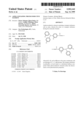
- the azine selected is a compound having the molecular formula: ##STR2## wherein R 1 -R 6 can be different or the same constituents, selected from the group consisting of hydrogen and C 1 -C 4 alkyl groups.
- a particular advantage of these transport layers with a transport substance and azine is that the crystallization sensitivity, i.e., the tendency for crystallization of the transport substance in the transport layer binder, is drastically reduced.
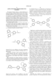
- the transport substance in the photoconductive elements is selected from the group consisting of tri-aryl amines and substituted stilbenes, such as compounds in accordance with the following general formula: ##STR3## where R 7 , R 9 and R 010 may be different or the same substituents, selected from C 1 -C 4 alkyl groups, and R 8 may be a hydrogen atom, a C 1 -C 4 alkyl group, an aryl group, an aryl group or an alkyl substituted aryl group.
- the photoconductive elements selected are preferably those having as stilbene a compound in which R 7 , R 9 and R 10 represents a hydrogen atom and R 10 a hydrogen atom or a methyl group.
- Single-layer or multi-layer photoconductive elements can be used in the invention.
- a charge-generating pigment, a transport substance and azine are applied in one layer to a conductive substrate.
- Multi-layer photoconductive elements of this kind are referred to, for example, in U.S. Pat. Nos. 3,713,820; 3,725,058; 3,824,099; 3,837,851; 3,839,034; and 3,898,084.
- the radiation-sensitive compound or compounds in the charge-generating layer may be of an organic or inorganic type. Where an inorganic material is used, it is generally present in the form of finely divided particles in a binder or in the form of a homogeneous film obtained, for example, by vapor coating. Selenium is a frequently used inorganic material. If an organic material is used it may, for example, be present in the form of a film-forming organic polymer, such as, for example, polyvinyl carbazole or polyvinyl pyrene or in the form of finely divided pigment particles dispersed in a binder such as, for example, Phenelac Blue and derivatives of this compound.
- a film-forming organic polymer such as, for example, polyvinyl carbazole or polyvinyl pyrene
- finely divided pigment particles dispersed in a binder such as, for example, Phenelac Blue and derivatives of this compound.
- pigment binder layers of this kind have a number of disadvantages in respect of uniformity and controllability of the photoelectric properties.
- Methods are therefore proposed in which the radiation-sensitive charge-generating pigments are applied in molecular divided form.
- the advantage of this technique is that the charge-generating layers can be thinner and smoother than the pigment binder layers.
- Charge-generating layers which contain radiation-sensitive compounds in molecular divided form are, for example, referred to in U.S. Pat. Nos. 4,123,270 and 4,286,040, and GB-A-1 172 355.
- organic photoconductive pigments such as perylene pigments, bisazo pigments, quinone pigments and phthalocyanine pigments. Pigments of this kind can easily be vaporized and then applied to a suitable substrate in order to obtain extremely thin homogeneous charge-generating layers. A charge transport layer is then applied to these layers and possibly a hard protective top layer.
- the charge transport layer must permit transport for charge carriers such as, for example, holes.
- the transport substances can be dissolved in a suitable binder for the purpose, such as polycarbonate (for example LexanTM, ICI and polyester carbonates).
- the substrate may contain an organic layer such as Mylar (du PontTM) or Melinex (ICITM) or another substrate suitable for the purpose, a semi-conductive layer or a conductive layer such as aluminum, chromium, nickel, etc.
- the polymeric substrate can be made conductive by the application of one or more thin metal layers such as aluminum, chromium, nickel, etc.
- the substrate may be a metal roller or a flexible endless strip of paper or plastic.
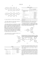
- Example 1 is a photoconductive element having a perylene generating layer above which is a transport layer which contains tritolylamine (TTA).
- TTA tritolylamine
- This photoconductive TTA element initially has a reasonably high Vrest, which is greatly increased after just 1 hour exposure to ambient light (TL light).
- TL light ambient light
- the initial Vrest is lowered somewhat, while after 1 hour exposure to ambient light the Vrest light is increased. This value is hardly increased even after exposure to light in a copier or printer.
- the photoconductive elements according to the invention have the advantage that the properties remain substantially constant after long periods of use and it is much easier to handle the material outside the copier or printer in ambient light.
- Azines according to the above-mentioned Japanese Patent Application are unsuitable.
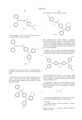
- TTA and an azine-2 in accordance with the molecular formula ##STR8## and in Examples 6 and 7 TTA and another azine-3 in accordance with the molecular formula: ##STR9## were added in various ratios. At the very start these photoconductive elements already had an unacceptably high Vrest.
- Photoconductive elements according to Examples 8 and 9 contain a vapor-coated perylene layer as generating layer and a transport layer containing a stilbene.
- Stilbene-1 has the molecular formula: ##STR10## and stilbene-2 has a the molecular formula: ##STR11##
- These photoconductive elements exhibit a considerable Vrest deterioration after exposure to CAT light. This deterioration was completely eliminated after adding a small quantity of azine-l to these stilbenes. These photoconductive elements do not exhibit any deterioration even after exposure to the ambient light.
- Examples 12 and 13 contain an evaporated perlene layer as a generation layer and a thin transporting layer containing a tri-aryl amine, TAPC, TAPC has the general formula: ##STR12##
- the photoconductor of example 12 also shows a large increase in the Vrest value after exposure to TL light. When azine-1 is added in a small amount, this increase is clearly eliminated (Example 13).
- the quantity of azine can be varied within wide limits (from about 2% by weight to 50% by weight).
- the stilbenes can also be mixtures of cis and transisomers around the olefinic fragment: ##STR13##
- the tetrahydronaphthyl group can be fixed to the nitrogen atom of the tertiary amino group at various places.
Landscapes
- Physics & Mathematics (AREA)
- General Physics & Mathematics (AREA)
- Photoreceptors In Electrophotography (AREA)
- Light Receiving Elements (AREA)
Abstract
Description
              TABLE
______________________________________
                     Start
                     Vrest  DO   Vrest
                                      After light
Ex.                  (V)    (%)  Start
                                      Exposure
______________________________________
 1   TTA             48     13   275  After 1 hour
                                      TL light
 2   TTA:Azine 1 = 95:5
                     44     11   60   After 1 hour
                                      TL light
 3   TTA:Azine 1 = 75:25
                     35     8    46   After 1 hour
                                      TL light
 4   TTA:Azine 2 = 95:25
                     142    13   --
 5   TTA:Azine 2 = 75:25
                     444    27   --
 6   TTA:Azine 3 = 95:25
                     70     12   --
 7   TTA:Azine 3 = 75:25
                     197    16   --
 8   Stilbene-1      27     9    107  After 100 hours
                                      CAT light
 9   Stilbene-2      26     8    149  After 100 hours
                                      CAT light
10   Stilbene-1:Azine-1 = 34:2
                     27     12   21   After 44 hours
                                      CAT light
11   Stilbene-2:Azine-1 = 34:2
                     28     10   28   After 60 hours
                                      CAT light
 12* TAPC            0.7    2    8.1  After 1 hour
                                      TL light
 13* TAPC:Azine 1 = 35:5
                     0.8    2    0.5  After 1 hour
                                      TL light
______________________________________
 --Not determined.
 *OPC with a 10μ transporting layer charged to -150 V usable with
 monocomponent toner.
 Vrest is the ASV (apparatus surface voltage) remaining after exposure of
 photoconductive element charged to -800 V, to 15 mJ/m.sup.2 white light
 DO (%) is the dark discharge in the first 2 seconds after charging.
Claims (7)
Applications Claiming Priority (2)
| Application Number | Priority Date | Filing Date | Title |
|---|---|---|---|
| NL1006695 | 1997-07-31 | ||
| NL1006695A NL1006695C2 (en) | 1997-07-31 | 1997-07-31 | Azine-containing photoconductive element. |
Publications (1)
| Publication Number | Publication Date |
|---|---|
| US5952142A true US5952142A (en) | 1999-09-14 |
Family
ID=19765432
Family Applications (1)
| Application Number | Title | Priority Date | Filing Date |
|---|---|---|---|
| US09/127,044 Expired - Lifetime US5952142A (en) | 1997-07-31 | 1998-07-31 | Azine-containing photoconductive element |
Country Status (5)
| Country | Link |
|---|---|
| US (1) | US5952142A (en) |
| EP (1) | EP0895128A1 (en) |
| JP (1) | JPH1172935A (en) |
| NL (1) | NL1006695C2 (en) |
| TW (1) | TW594450B (en) |
Cited By (3)
| Publication number | Priority date | Publication date | Assignee | Title |
|---|---|---|---|---|
| US6432597B1 (en) | 2000-12-08 | 2002-08-13 | Lexmark International, Inc. | Electrophotographic photoconductor containing fluorenyl-azine derivatives and triarylamine in transport layer |
| US20030186146A1 (en) * | 2001-12-27 | 2003-10-02 | Toyoko Shibata | Organic photoreceptor and image forming method |
| CN102902170A (en) * | 2011-07-28 | 2013-01-30 | 京瓷办公信息系统株式会社 | Electrophotographic photoreceptor using diphenylvinyl triphenylamine derivatives and imaging forming apparatus |
Families Citing this family (3)
| Publication number | Priority date | Publication date | Assignee | Title |
|---|---|---|---|---|
| JP2001296684A (en) * | 2000-04-11 | 2001-10-26 | Mitsubishi Chemicals Corp | Toner and method for image forming |
| JP2002040704A (en) * | 2000-05-19 | 2002-02-06 | Mitsubishi Chemicals Corp | Image forming method and image forming device |
| JP2002049164A (en) * | 2000-05-22 | 2002-02-15 | Mitsubishi Chemicals Corp | Method for forming image and device for image formation |
Citations (12)
| Publication number | Priority date | Publication date | Assignee | Title |
|---|---|---|---|---|
| GB1172355A (en) * | 1966-12-12 | 1969-11-26 | Renker Belipa Gmbh | Electrophotographic Recording Materials |
| US3713820A (en) * | 1971-09-07 | 1973-01-30 | Ibm | Electrophotographic charge transport layer |
| US3725058A (en) * | 1969-12-30 | 1973-04-03 | Matsushita Electric Ind Co Ltd | Dual layered photoreceptor employing selenium sensitizer |
| US3824099A (en) * | 1973-01-15 | 1974-07-16 | Ibm | Sensitive electrophotographic plates |
| US3837851A (en) * | 1973-01-15 | 1974-09-24 | Ibm | Photoconductor overcoated with triarylpyrazoline charge transport layer |
| US3839034A (en) * | 1972-07-31 | 1974-10-01 | Kalle Ag | Electrophotographic recording material |
| US3898084A (en) * | 1971-03-30 | 1975-08-05 | Ibm | Electrophotographic processes using disazo pigments |
| US4123270A (en) * | 1975-09-15 | 1978-10-31 | International Business Machines Corporation | Method of making electrophotographic imaging element |
| US4286040A (en) * | 1978-08-14 | 1981-08-25 | Oce-Nederland B.V. | Process for preparing an electrophotographic element |
| US4420548A (en) * | 1980-11-28 | 1983-12-13 | Canon Kabushiki Kaisha | Electrophotographic member with hydrazone or ketazine compounds |
| US4777296A (en) * | 1984-02-21 | 1988-10-11 | Ricoh Company, Ltd. | Styryl derivatives and electrophotographic photoconductor comprising one styryl derivative |
| US4784929A (en) * | 1986-05-21 | 1988-11-15 | Minolta Camera Kabushiki Kaisha | Photosensitive member with hydrazone and/or azine charge transport material |
Family Cites Families (5)
| Publication number | Priority date | Publication date | Assignee | Title |
|---|---|---|---|---|
| NL8200331A (en) * | 1982-01-29 | 1983-08-16 | Oce Nederland Bv | MULTILAYER ELECTROPHOTOGRAPHIC ELEMENT. |
| JPS60196765A (en) * | 1984-03-21 | 1985-10-05 | Tomoegawa Paper Co Ltd | Electrophotographic sensitive body |
| JPS6143752A (en) * | 1984-08-08 | 1986-03-03 | Minolta Camera Co Ltd | Photosensitive material |
| JPS61212847A (en) * | 1985-03-18 | 1986-09-20 | Minolta Camera Co Ltd | Photosensitive body |
| DE69509187T2 (en) * | 1994-10-31 | 1999-09-16 | Hodogaya Chemical Co. Ltd., Kawasaki | Tetrahydronaphthylaminostyrene compounds and their use in electrophotographic photoreceptors |
-
1997
- 1997-07-31 NL NL1006695A patent/NL1006695C2/en not_active IP Right Cessation
-
1998
- 1998-03-24 TW TW087104370A patent/TW594450B/en not_active IP Right Cessation
- 1998-07-08 EP EP98202306A patent/EP0895128A1/en not_active Withdrawn
- 1998-07-16 JP JP10201719A patent/JPH1172935A/en active Pending
- 1998-07-31 US US09/127,044 patent/US5952142A/en not_active Expired - Lifetime
Patent Citations (12)
| Publication number | Priority date | Publication date | Assignee | Title |
|---|---|---|---|---|
| GB1172355A (en) * | 1966-12-12 | 1969-11-26 | Renker Belipa Gmbh | Electrophotographic Recording Materials |
| US3725058A (en) * | 1969-12-30 | 1973-04-03 | Matsushita Electric Ind Co Ltd | Dual layered photoreceptor employing selenium sensitizer |
| US3898084A (en) * | 1971-03-30 | 1975-08-05 | Ibm | Electrophotographic processes using disazo pigments |
| US3713820A (en) * | 1971-09-07 | 1973-01-30 | Ibm | Electrophotographic charge transport layer |
| US3839034A (en) * | 1972-07-31 | 1974-10-01 | Kalle Ag | Electrophotographic recording material |
| US3824099A (en) * | 1973-01-15 | 1974-07-16 | Ibm | Sensitive electrophotographic plates |
| US3837851A (en) * | 1973-01-15 | 1974-09-24 | Ibm | Photoconductor overcoated with triarylpyrazoline charge transport layer |
| US4123270A (en) * | 1975-09-15 | 1978-10-31 | International Business Machines Corporation | Method of making electrophotographic imaging element |
| US4286040A (en) * | 1978-08-14 | 1981-08-25 | Oce-Nederland B.V. | Process for preparing an electrophotographic element |
| US4420548A (en) * | 1980-11-28 | 1983-12-13 | Canon Kabushiki Kaisha | Electrophotographic member with hydrazone or ketazine compounds |
| US4777296A (en) * | 1984-02-21 | 1988-10-11 | Ricoh Company, Ltd. | Styryl derivatives and electrophotographic photoconductor comprising one styryl derivative |
| US4784929A (en) * | 1986-05-21 | 1988-11-15 | Minolta Camera Kabushiki Kaisha | Photosensitive member with hydrazone and/or azine charge transport material |
Cited By (6)
| Publication number | Priority date | Publication date | Assignee | Title |
|---|---|---|---|---|
| US6432597B1 (en) | 2000-12-08 | 2002-08-13 | Lexmark International, Inc. | Electrophotographic photoconductor containing fluorenyl-azine derivatives and triarylamine in transport layer |
| US20030186146A1 (en) * | 2001-12-27 | 2003-10-02 | Toyoko Shibata | Organic photoreceptor and image forming method |
| US20050037273A1 (en) * | 2001-12-27 | 2005-02-17 | Toyoko Shibata | Organic photoreceptor and image forming method |
| US6919155B2 (en) * | 2001-12-27 | 2005-07-19 | Konica Corporation | Organic photoreceptor and image forming method |
| US7074539B2 (en) * | 2001-12-27 | 2006-07-11 | Konica Corporation | Organic photoreceptor and image forming method |
| CN102902170A (en) * | 2011-07-28 | 2013-01-30 | 京瓷办公信息系统株式会社 | Electrophotographic photoreceptor using diphenylvinyl triphenylamine derivatives and imaging forming apparatus |
Also Published As
| Publication number | Publication date |
|---|---|
| EP0895128A1 (en) | 1999-02-03 |
| NL1006695C2 (en) | 1999-02-02 |
| JPH1172935A (en) | 1999-03-16 |
| TW594450B (en) | 2004-06-21 |
Similar Documents
| Publication | Publication Date | Title |
|---|---|---|
| US4407919A (en) | Electrophotographic plate | |
| US4396695A (en) | Electrophotographic medium with heterocyclic azo photoconductor | |
| US5952142A (en) | Azine-containing photoconductive element | |
| US4397931A (en) | Stabilized organic layered photoconductive device | |
| JPH07134430A (en) | Electrophotographic photoreceptor | |
| US6472514B2 (en) | Electron transport compounds | |
| US5330865A (en) | Multi-layered electrophotographic element having a mixture of perylene pigments | |
| JP2000143607A (en) | Electron transporting material, electrophotographic photoreceptor and electrophotographic apparatus | |
| US5567557A (en) | Electrophotographic photoreceptor | |
| US6268095B1 (en) | Photoconductor for electrophotography | |
| US5888685A (en) | Electrophotographic photoconductor | |
| US5166019A (en) | Photosensitive member comprising specified distyryl compound as charge transporting material | |
| US4567125A (en) | Electrophotographic recording material | |
| US5968697A (en) | Electrophotographic photoconductor | |
| US4932860A (en) | Electrophotographic photosensitive member | |
| US5945243A (en) | Photoconductor for electrophotography and method of manufacturing the same | |
| US5061584A (en) | Electrophotographic photoreceptor | |
| US5972549A (en) | Dual layer photoconductors with charge generation layer containing hindered hydroxylated aromatic compound | |
| US5213925A (en) | Photoconductor for electrophotography | |
| JPH07160023A (en) | Electrophotographic photoreceptor | |
| JPH07244390A (en) | Electrophotographic photoconductor | |
| US5252416A (en) | Photoconductor for electrophotography | |
| JPH07306536A (en) | Electrophotographic photoconductor | |
| JPH0882941A (en) | Electrophotographic photoreceptor | |
| JPH02160248A (en) | Electrophotographic sensitive body |
Legal Events
| Date | Code | Title | Description |
|---|---|---|---|
| AS | Assignment |
Owner name: OCE-TECHNOLOGIES, B.V., NETHERLANDS Free format text: ASSIGNMENT OF ASSIGNORS INTEREST;ASSIGNORS:DERKS, PETRUS JOHANNES MARIA;PERSOON, ACHILLES WILHELMUS MARIA;VAN HORCK, MARIA PETRONELLA HENRICA;REEL/FRAME:009504/0088 Effective date: 19980722 |
|
| FEPP | Fee payment procedure |
Free format text: PAYOR NUMBER ASSIGNED (ORIGINAL EVENT CODE: ASPN); ENTITY STATUS OF PATENT OWNER: LARGE ENTITY |
|
| STCF | Information on status: patent grant |
Free format text: PATENTED CASE |
|
| FPAY | Fee payment |
Year of fee payment: 4 |
|
| FPAY | Fee payment |
Year of fee payment: 8 |
|
| FEPP | Fee payment procedure |
Free format text: PAYER NUMBER DE-ASSIGNED (ORIGINAL EVENT CODE: RMPN); ENTITY STATUS OF PATENT OWNER: LARGE ENTITY Free format text: PAYOR NUMBER ASSIGNED (ORIGINAL EVENT CODE: ASPN); ENTITY STATUS OF PATENT OWNER: LARGE ENTITY |
|
| FPAY | Fee payment |
Year of fee payment: 12 |